

Page 1
T-51383L070J-FW-P-AA
OPTREX CORPORATION Page-
1/22
LCD Module Technical Specification
T-51383L070J-FW-P-AA
Table of Contents
1. Applications
...........................................................................................................................................................
2
2. Features
.....................................................................................................................................................................
2
3. Mechanical Specifications
.........................................................................................................................
2
4. Mechanical Drawing TFT LCD Module
.....................................................................................
3
5. Input / Output Terminals
..........................................................................................................................
4
6. Absolute Maximum Ratings
.....................................................................................................................
6
7. Electrical Characteristics
...............................................................................................................................
6
8. Power Sequence
.........................................................................................................................................
15
9. Optical Characteristics
................................................................................................................................
16
10. Handing Cautions
...........................................................................................................................................
17
11. Reliability TEST
.............................................................................................................................................
22
12. Block Diagram
....................................................................................................................................................
23
Checked by (Design Engineering Div.)
Checked by (Quality Assurance Div.)
Prepared by (Production Div.)
Revision History
Rev. Date Page Comment
First Edition
Jan 1, 2001
Final Revision
******
OPTREX
Page 2
T-51383L070J-FW-P-AA
OPTREX CORPORATION Page-
2/22
1. Application
This technical specification applies to 7.0” color TFT-LCD module. The applications of the
panel are car TV, portable DVD,GPS, m ultimedia applications and others AV system.
2. Features
. Compatible with NTSC & PAL system
. Pixel in stripe configuration
. Slim and compact
. High Brightness
. Image Reversion:Up/Down and Left/Right
. Multi Video Display Mode
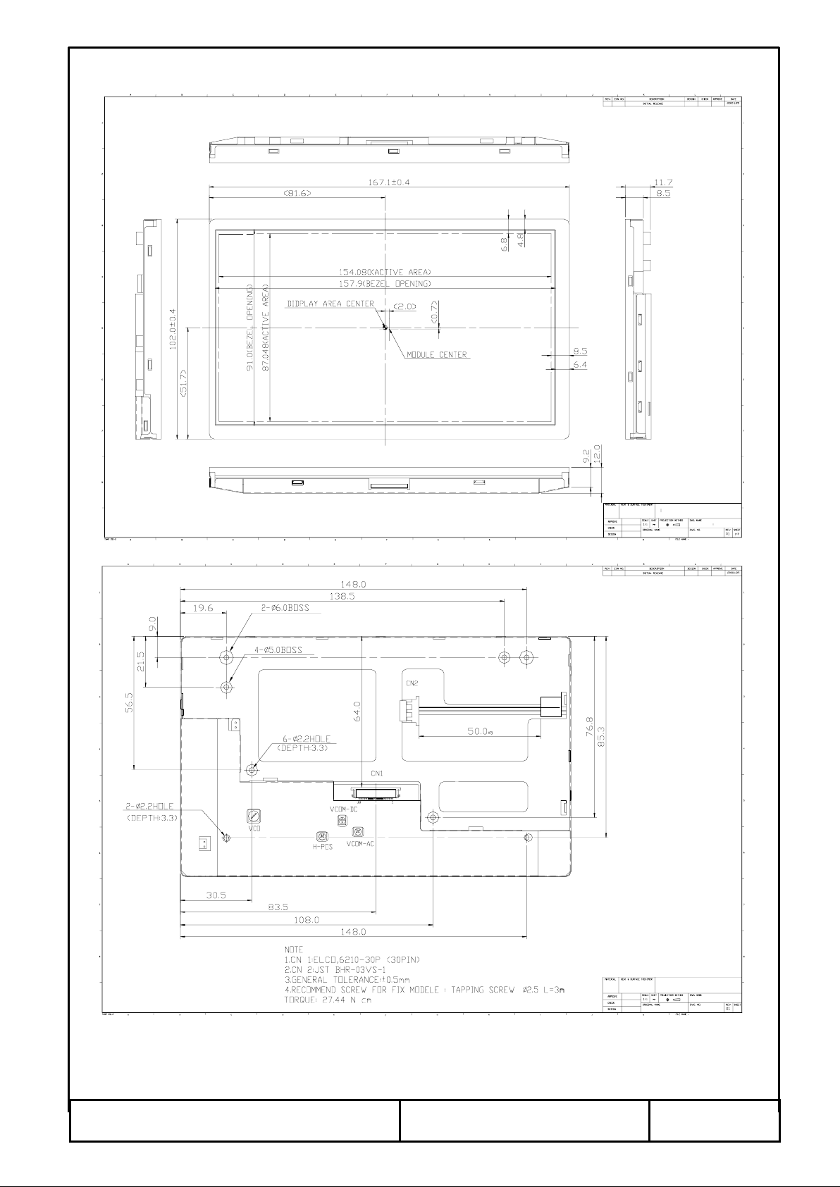
3. Mechanical Specifications
Parameter Specifications Unit
Screen Size 7.0 (16:9 diagonal) inch
Display Format
1440 (H) ×234(V)
dot
Active Area
154.08 (H)×87.05 (V)
mm
Dot Pitch
0.107(H)×0.372 (V)
mm
Pixel Configuration Stripe
Outline Dimension 167.1 (W )×102.0 (H)×12.0 (D)(typ.) mm
Surface Treatment Anti-Glare and Hard Coating
Weight
205±10
g
Page 3
T-51383L070J-FW-P-AA
OPTREX CORPORATION Page-
3/22
4. Mechanical Drawing of TFT-LCD Module
Page 4
T-51383L070J-FW-P-AA
OPTREX CORPORATION Page-
4/22
5. Input / Output Terminals
5-1) TFT-LCD Panel Driving
The interface connector is 6210-30P Series manufactured by ELCO or equivalent.
(0.5mm pitch 30 pin)
The connector interface pin assignments are listed in the Table below.
Pin No
Symbol
I/O Description Remark
1
PSI
O Synchronize Pulse for Decoder
2
V
R
I Red Video Input
3
V
G
I Green Video Input
4
V
B
I Blue Video Input
5
GND
I Ground
6
CSY
I Composite Sync Input
7
NC
No Connection
8
NC
No Connection
9
NC
No Connection
10
NC
No Connection
11
MODE 1
I Display mode selection pin 1 (refer to 5.2)
12
MODE 2
I Display mode selection pin 2 (refer to 5.2)
13
MODE 3
I Display mode selection pin 3 (refer to 5.2)
14
GND
I Ground
15
BLK
O Video Signal Mask Timing Output
16
HSY
O Horizontal Sync Output
17
VSY
O Vertical Sync Output
18
V
DD
I Input Voltage For Logic/Logic Voltage For Source Driver
19
NC
No Connection
20
FRP
O Video Polarity Control Signal
21
GND
I Ground
22
U/D
I Scanning Direction : (Low : Normal , High : Reverse)
23
L/R
I Scanning Direction : (Low : Normal , High : Reverse)
24
N/P
I NTSC/PAL Selection Signal(Low : PAL , Hig h : NTSC)
25
NC
No Connection
26
NC
No Connection
27
GND
I Ground
28 V
CC
I Analog Voltage For Source Driver/Logic Voltage For Gate
29 V
GH
I Positive Voltage For Gate Driver
30 V
GL
INegative Voltage For Gate Driver
Page 5
T-51383L070J-FW-P-AA
OPTREX CORPORATION Page-
5/22
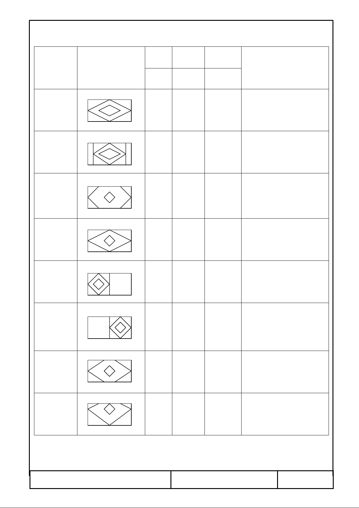
5.2)Display Mode
NO:11 NO:12 NO:13
Display Mode
Display (Input Signal
of 4:3 Aspect Ratio)
Mode 1 Mode 2 Mode 3
Note
Full
Low
Low Low
Input Video Signals Are
Displayed In Full Screen.
Normal
Center
High Low Low
Input Video Signals Are
Displayed In The Center
Screen.(4:3 Aspect Ratio)
Zoom 1 High High Low
Input Video Signal Of
Central 176 Lines Are
Display In Full
Screen.(Vertically Extension)
Wide Low High Low
Input Video Signals Are
Displayed In Full Screen.
(Horizontal Modification)
Normal Left High Low High
Input Video Signals Are
Display In the Left Screen.
(4:3 Aspect Ratio)
Normal Right
Low
High High
Input Video Signals Are
Display In the Right Screen.
(4:3 Aspect Ratio)
Zoom 2 Low Low High
I
nput Video Signal Of
Central 204 Lines Are
Display In Full
Screen.(Vertically Extension
Zoom 3
High
High High
Same As Zoom 2 Mode
Vertically Offset Centered
Page 6
T-51383L070J-FW-P-AA
OPTREX CORPORATION Page-
6/22
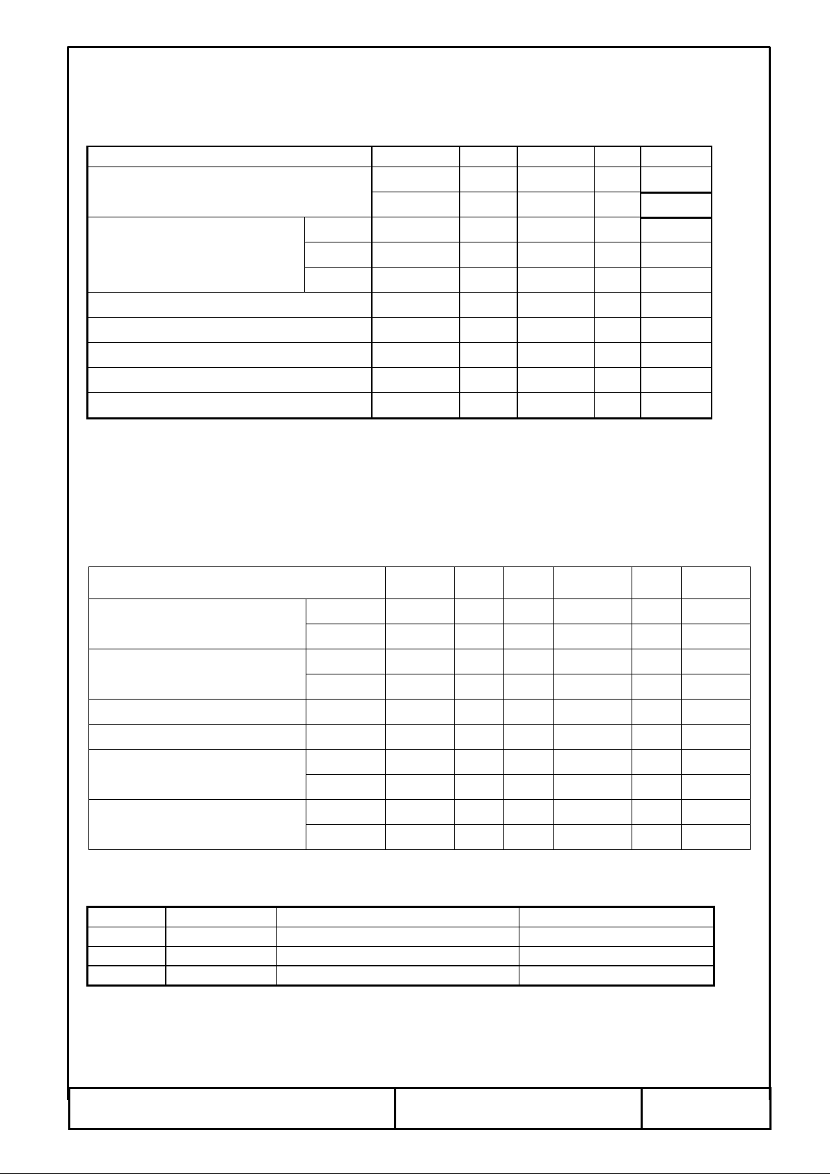
6
Absolute Maximum Ratings:
The followings are maximum values , which if exceeded, may cause faulty operat ion or dam age
to the unit.
Parameter Symbol MIN. MAX. Unit Remark
V
CC
-0.5 7 V
Supply Voltage For Source Driver
V
DD
-0.5 7 V
V
GH- VGL
-0.3 40 V
H Level V
GH
040 V
Supply Voltage For Gate Driver
L Level
V
GL
-20
0V
Analog Signal Input Level VR,VG,V
B
-0.3 7.0 V Note 6-1
Digital Input Signals -0.3 5.5 V
Digital Output Signals -0.3 5.5 V
Storage Temperature -30 +80
℃
Operation Temperature -20 +70
℃
Note 6-2
Notes:6-1 Analog Input Voltage means VR,VG,VB.
Notes:6-2 Operating Tem perature define that contrast, response time, other display
optical character are Ta=+25.
7
Electrical Characteristics
7-1) Recommended Driving condition for TFT-LCD panel
Parameter
Symbol MIN. Typ MAX Unit Remark
Analog V
CC
4.5 5.0 5.5 V
Supply Voltage For Source
Driver
Logic V
DD
4.5 5.0 5.5 V
H level V
GH
+15 +17 +19 V
Supply Voltage For Gate Driver
L level V
GL
-16 -15 -14 V
Supply Voltage For controller
V
DD
4.5 5.0 5.5 V
Analog Signal input Level
Amplitude 0.3 V
CC-
0.3 V
H level V
IN
0.7
-VDDV
Digital input voltage
L level V
IL
-0.3 - 0.3 V
DD
V
H level V
OH
0.7
-VDDV
Digital output voltage
L level V
OL
-0.3 - 0.3 V
DD
V
7-2) Backlight driving & Power Consumpt ion
Pin No Symbol Description Remark
1 VL1 Input terminal (Hi voltage side) Wire color: pink
2 NC No Connection
3 VL2 Input ter minal (Low voltage side) Wire color: white Note 7-1
Page 7
T-51383L070J-FW-P-AA
OPTREX CORPORATION Page-
7/22
Note 7-1:Low voltage side of backlight inverter connect s with Gr ound of inverter circuits.
Recommended Driving condition for backlight Ta= 25
℃
Parameter Symbol Min. Typ. Max. Unit Remark
Lamp voltage V
L
810 Vrms IL=6mA
Lamp current I
L
4.5 6 7 mA
Lamp frequency P
L
35 60 KHz Note 7-2
Kick-off voltage(25
℃
)
Vs TBD TBD 1095 Vrms Note 7-3
Kick-off voltage(0
℃
)
Vs TBD TBD 1340 Vrms Note 7-3
Note 7-2 : The waveform of lam p driving voltage should be as closed to a perfect sine wave as
possible.
Note 7-3 : The Kick-off times≧1sec.
Power Consumption Ta= 25
℃
Parameter Symbol Conditions TYP. MAX Unit Remark
Supply current for Gate Dr iver ( Hi level) I
GH
V
GH
=
+17V
0.15 0.2 mA
Supply current for Gate Dr iver ( Low level) I
GL
V
GL
=
-15V
20 50 mA
Supply current for Source Driver I
CC
VCC = +5V
20 30 mA
Supply current for controller I
DD
VDD = +5V
20 30 mA
LCD Panel Power Consumption 0.50 W Note 7-4
Backlight Lamp Power Consumption 4.86 W Note 7-5
Note 7-4:The power consumption for backlig ht is not included.
Note 7-5:Backlight lamp power consumption is calculated by I
L
×
V
L
.
7-4) Input / Output Connector
A) LCD Module Connector
The interface connector is 6210-30p Ser ies m anufactured by Elco or equivaleut
(0.5mm pitch 30pin)
B) Backlight Connector, JST BHR-03VS-1. Pin No.:3, Pitch:4 mm
7-5) Pixel Arrangement and Output Interface Pin
123456
1438 1439 1440
1RGBRGB RGB
2RGBRGB RGB
3RGBRGB RGB
233RGBRGB RGB
234RGBRGB RGB
Page 8

T-51383L070J-FW-P-AA
OPTREX CORPORATION Page-
8/22
7-6)Signal Timing Waveforms
Timing Specification
[Horizontal]
Parameter Symbol Condition NTSC PAL Unit Notes
Horizontal Start
Position
HPOS - 11.35 11.54 usec Note7-6
Horizontal Display
Area
HDIS - 50.01 50.36 usec
Notes :7-6
1. Sampling start based on the composite sync falling edg e.
2. This value is default , if you want to charge ,please contact PVI.
[Vertical]
Display Mode
Paramet
er
Symbol Condition
Full
Normal
Wide
Zoom1Zoom2Zoom
3
Unit Notes
NTSC ODD
EVEN
22
286
22
286
52
315
38
301
53
315
Line Note 7-7
Vertical
Start
Position
VPOS
PAL ODD
EVEN
26
339
26
363
62
375
50
363
62
375
Line Note 7-7
NTSC 234 234 176 204 204 Line
Vertical
Display
Position
VDIS
PAL 281 281 210 234 234 Line
Notes :7-7 Sampling start line number base on the vertical sync pulse (SYNC).
4.67(4.70)usec
SYNC 1.0 Vp-p
3.12(3.32)usec
5V
HSY
0V
4.67(4.70)usec
1 Line = 63.56 (64.00)usec
+0.7V
R,G,B
0V
50.01(50.36)usec
Display Area
11.35(11.54)usec
Note:7-7 Values in brackets correspond to PAL mode (fH=15.734(15.625)KHZ ).
Page 9

T-51383L070J-FW-P-AA
OPTREX CORPORATION Page-
9/22
7-7) Display Time Range
A)
When sync. signal of NTSC system is applied.
a)
Horizontally
11.35 ~ 61.36 μs.
b)
Vertical
22 ~ 255 H
B) When sync. signal of PAL system is applied.
a)
Horizontally
11.54 ~ 61.9μs
b)
Vertical
28 ~ 300 H
Page 10

T-51383L070J-FW-P-AA
OPTREX CORPORATION Page-
10/22
C) NTSC System Timing Reference
Tvo=254£gS Typ
Vin
CSY
HSY
VSY
FRP
RGB
ODD
FIELD
EVEN
FIELD
ODD FIELD
524 525 1 2 3 4 5 6 7 8 9 10 23 24 25 26
NTSC FIELD 1
CMOS output
258 259 260 261 262 1 2 3 4 5 6 7 20 21 22 23
Th Th=63.5£gS Typ
Tvo
Tvpo=63.5£gS Typ
Tvpo
Black
Black
White
White
First
Line
Timing chart of I/O and RGB signal
Page 11

T-51383L070J-FW-P-AA
OPTREX CORPORATION Page-
11/22
262 263 264 265 266 267 268 269 270 271 272 285 286 287 288
NTSC FIELD 2
EVEN FIELD
Vin
CSY
HSY
VSY
FRP
RGB
First
line
EVEN
FIELD
ODD
FIELD
259 260 261 262 263 1 2 3 4 5 6 20 21 2219
Tvo=254£gS Typ
Tvo
Tvpe=95£gS Typ
Tvpe
Timing chart of I/O and RGB signal
White
White
Black
Black
Page 12

T-51383L070J-FW-P-AA
OPTREX CORPORATION Page-
12/22
D) PAL System Timing Reference
Tvo=318£gS Typ
Vin
CSY
HSY
VSY
FRP
RGB
ODD
FIELD
EVEN
FIELD
ODD FIELD
622 623 624 625 1 2 3 4 5 6 7 23 24 25 26
PAL
CMOS output
310 311 312 313 1 2 3 4 5 6 7 21 23 24 25
Th
Th=63.5£gS Typ
Tvo
Tvpo=64£gS Typ
Tvpo
First
Line
Timing chart of I/O and RGB signal
FIELD 1
21
22
22
26
27
28
Black
White
Black
White
2827
Page 13

T-51383L070J-FW-P-AA
OPTREX CORPORATION Page-
13/22
309 310 311 312 313 314 315 316 317 318 336 337 338 339
CSY
HSY
VSY
FRP
RGB
First
line
EVEN
FIELD
ODD
FIELD
308 309 310 311 312 1 2 3 4 5 24 25 26
Black
23
Tvo=318£gS Typ
Tvo
Tvpe=32£gS Typ
Tvpe
Timing chart of I/O and RGB signal
335
22 27
28
2
9
340
341
White
White
Black
White
White
Black
Page 14

T-51383L070J-FW-P-AA
OPTREX CORPORATION Page-
14/22
E) Display Timing (NTSC)
Tvo=254£gS Typ
Vin
CSY
HSY
VSY
FRP
RGB
ODD
FIELD
EVEN
FIELD
ODD FIELD
524 525 1 2 3 4 5 6 7 8 9 10 23 24 25 26
NTSC FIELD 1
CMOS output
258 259 260 261 262 1 2 3 4 5 6 7 20 21 22 23
Th Th=63.5£gS Typ
Tvo
Tvpo=63.5£gS Typ
Tvpo
Black
Black
White
White
First
Line
Timing chart of I/O and RGB signal
Page 15

T-51383L070J-FW-P-AA
OPTREX CORPORATION Page-
15/22
F) Display Timing (PAL)
11.54
µ
s
Tho=4.7µs
64µs
2.1µs
50.36
µ
s
50.36/64=79%
Display Time
Sampling Clock: 9.53MHz
(1) Horizontal Timing
(2) Vertical Timing
Vin
ODD
FIELD
EVEN
FIELD
ODD FIELD
622 623 624 625 1 2 3 4 5 6 7 22 23 24 25
PAL FIELD 1
20
21
Tvo=5H Typ
VSY
Tvo
Tvpo=1H Typ
Tvpo
309 310 311 312 313 314 315 316 317
318
334 335 336
33
7
PAL FIELD 2
EVEN FIELD
Vin
EVEN
FIELD
ODD
FIELD
333
338 339
VSY
Tvo=5H Typ
Tvo
Tvpe=0.5H Typ
Tvpe
8.5H
28H
First
Line
234 H
Not Display Time
79.4/317.5=25%
Display Time
234/317.5=75%
28.5H
Page 16

T-51383L070J-FW-P-AA
OPTREX CORPORATION Page-
16/22
8.Power Sequence
1) 10ms≦T1≦T2≦T3
2) 10ms≦T4≦T5≦T6
0V(Gnd)
V
GH
VCC,V
DD
V
GL
ON
OFF
T1
T2
T3 T4 T5 T6
OFF
Logic,VCom,
Videosignal
Page 17

T-51383L070J-FW-P-AA
OPTREX CORPORATION Page-
17/22
9.Optical Characteristics
9-1) Specification:
Ta = 25
℃
Parameter Symbol ConditionMIN. TYP. MAX. Unit Remarks
Viewing Horizontal
θ
21, θ22
45 55 deg Note 9-1
Angle Vertical
θ
12 CR≧10
10 15 deg Note 9-1
θ
11
30 35 deg Note 9-1
Contrast Ratio CR 70 150 Note 9-2
Response time Rise Tr
θ=0°
30 ms Note 9-4
Fall Tf 50 ms
Brightness 350 400
cd/
㎡
Note 9-3
White x 0.285 Note 9-3
Chromaticity y 0.295
Lamp Life Time
+25
℃
10,000 hr
Note 9-1: The definitions of viewing angles
Page 18

T-51383L070J-FW-P-AA
OPTREX CORPORATION Page-
18/22
Luminance when Testing point is White
Note 9-2:CR
=
Luminance when Testing point is Black
(Testing configuration see 8-2 )
Contrast Ratio is measured in optimum com m on elect rode voltage.
Note 9-3:Topcon BM-7(fast) luminance meter 2°field of view is used in the testing (af t er
20~30 minutes operation).
Lamp Current 6mA
Note 9-4: The definition of response time:
100%
90%
10%
0%
White White
Brightness
Black
Tr Tf
Page 19

T-51383L070J-FW-P-AA
OPTREX CORPORATION Page-
19/22
9-2) Testing configuration
y
LCD Display
y
R, G, B Waveform of Pattern A at Testing Point
y
R, G, B Waveform of Pattern B at Testing Point
500mm
BM-7(fast)
LCD
Backlight
R,G,B signal
Pattern
generator
input
Pattern A Pattern B
Testing Point Testing Point
16ms 16ms
16ms 16ms
Caution: 1. Environmental illumination≦1 lux
2. Before test CR, Vcom v oltage must
be adjusted carefully to get the best
CR.
Vcom
RGB
waveform
RGB
waveform
Vcom
Page 20

T-51383L070J-FW-P-AA
OPTREX CORPORATION Page-
20/22
10. Handling Cautions
10-1) Mounting of module
a) Please power off the module when you connect the input/output connector.
b) Please connect the ground pattern of the inverter circute surely. If the
connection is not perfect, some following problems may happen possibly.
1.The noise from the b acklight unit will increase.
2.The output from inverter circuit will be un stable.
3.In some cases a part of module will heat.
c) Polarizer which is made of soft material and susceptible to flaw must be
handled carefully.
d) Protective film (Laminator) is applied on surface to protect it against scratches
and dirts. It is recommended to peel off the laminator before use and taking
care of static electricity.
10-2) Precautions in mounting
a) When metal part of the TFT-LCD module (shielding lid and rear case) i s soi l ed,
wipe it with soft dry cloth.
b) Wipe off water drops or finger grease immediately. Long contact with water
may cause discoloration or spots.
c) TFT-LCD module uses glass which breaks or cracks easily if dropped or
bumped on hard surface. Please handle with care.
d) Since CMOS LSI is used in the module. So take care of static electricity and
earth yourself when handling.
10-3) Adjusting module
a) Adjusting volumes on the rear face of the module have been set optimally
before shipment.
b) Therefore, do not change any adjusted values. If adjusted values are changed,
the specifications described may not be satisfied.
10-4) Others
a) Do not expose the module to direct sunlight or intensive ultraviolet rays for
many Hours.
b) Store the module at a room temperature place.
c) T he voltage of beginning electric discharge may over the normal voltage
because of leakage current from approach conductor by to draw lump read
lead line around.
d) If LCD panel breaks, it is possibly that the liquid crystal escapes from the
panel.Avoid putting it into eyes or mouth. When liquid crystal sticks on hands,
clothes or feet. Wash it out immediately with soap.
e) Observe all other precautionary requirements in handling general electronic
components.
f) Please adjust the voltage of common electrode as material of attachment by 1
module.
Page 21

T-51383L070J-FW-P-AA
OPTREX CORPORATION Page-
21/22
11. Reliability Test
No Test Item Test Condition
1 High Temperature Stor age Test
Ta = +80 ℃, 240 hrs
2 Low Temperature Storage Test
Ta = -30℃, 240 hrs
3 High Temperature Operation Test
Ta = +70 ℃, 240 hrs
4 Low Temperature Oper at ion Test
Ta = -20 ℃, 240 hr s
5
High Temperature & High
Humidity Operation Test
Ta = +60℃, 95%RH, 240 hrs
6
Thermal Cycling Test
(non-operating)
-25℃ →+25℃→ +70℃, 200 Cycles
30 min 5min 30 min
7
Vibration Test
(non-operating)
Frequency:10 ~ 55 H
Z
Amplitude:1.5 mm
Sweep time: 11 mins
Test Period: 6 Cycles for each direction of X, Y, Z
8
Shock Test
(non-operating)
100G, 6ms
Direction: ±X, ±Y, ±Z
Cycle: 3 times
9
Electrostatic Discharge Test
(non-operating)
150pF, 330Ω
Air: ±15KV; Contact: ± 8KV
10 times/point, 9 points/panel face
Ta: ambient temperatur e
[Criteria]
Under the display quality test conditions with normal operation stat e, there should be no
change which may affect practical display function.
Page 22

T-51383L070J-FW-P-AA
OPTREX CORPORATION Page-
22/22
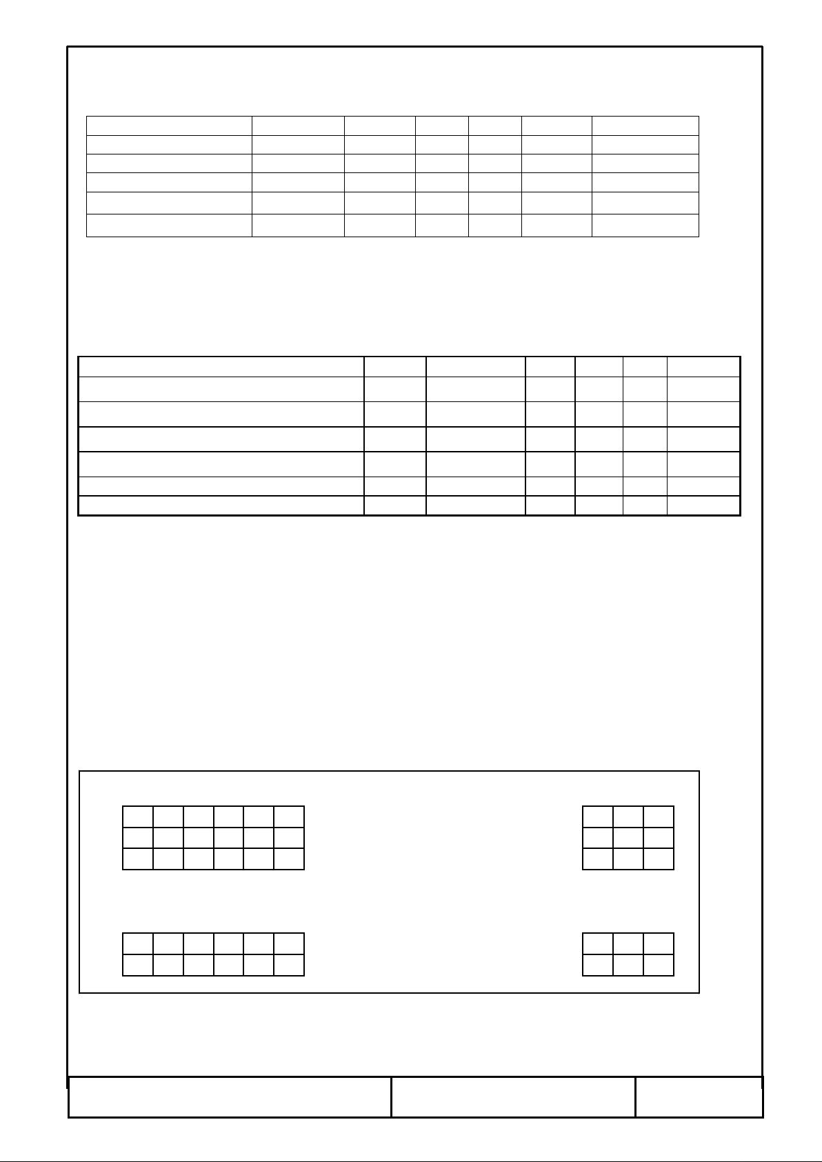
11. Block Diagram
Controller
VDriver
(Gate)
LCDPanel
HDriver
(Source)
Back-lightInverter
HSY
VSY
CSY
BLK
U/D
R/L
N/P
Mode1,2,3
FRP
+5V
+17V
-15V
VR
VG
VB
R1G1B1
VCO
PLL VL
 Loading...