

Page 1
TE
C
H
tm
T35L6464A
SYNCHRONOUS
BURST SRAM
FEATURES
•
Fast Access times: 5, 6, 7, and 8ns
• Fast clock speed: 100, 83, 66, and 50 MHz
•
Provide high performance 3-1-1-1 access rate
•
•
•
OE
Fast
Single 3.3V +10% / -5V power supply
Common data inputs and data outputs
• BYTE WRITE ENABLE and GLOBAL
WRITE control
•
Five chip enables for depth expansion and
address pipelining
•
Address, control, input, and output pipelined
registers
• Internally self-timed WRITE cycle
•
WRITE pass-through capability
•
Burst control pins ( interleaved or linear burst
sequence)
•
High density, high speed packages
•
Low capacitive bus loading
• High 30pF output drive capability at rated access
time
•
SNOOZE MODE for reduced power standby
•
Single cycle disable ( PentiumTM BSRAM
compatible )
OPTIONS
TIMING MARKING
5ns access/10ns cycle -5
6ns access/12ns cycle -6
7ns access/15ns cycle -7
8ns access/20ns cycle -8
Package
128-pin QFP Q
128-pin LQFP L
Part Number Examples
PART NO. Pkg. BURST SEQUENCE
T35L6464A-5Q Q Interleaved
T35L6464A-5L L Linear (MODE=GND)
access times: 5 and 6ns
(MODE=NC or VCC)
64K x 64 SRAM
3.3V SUPPLY, FULLY REGISTERED AND OUTPUTS,
BURST COUNTER
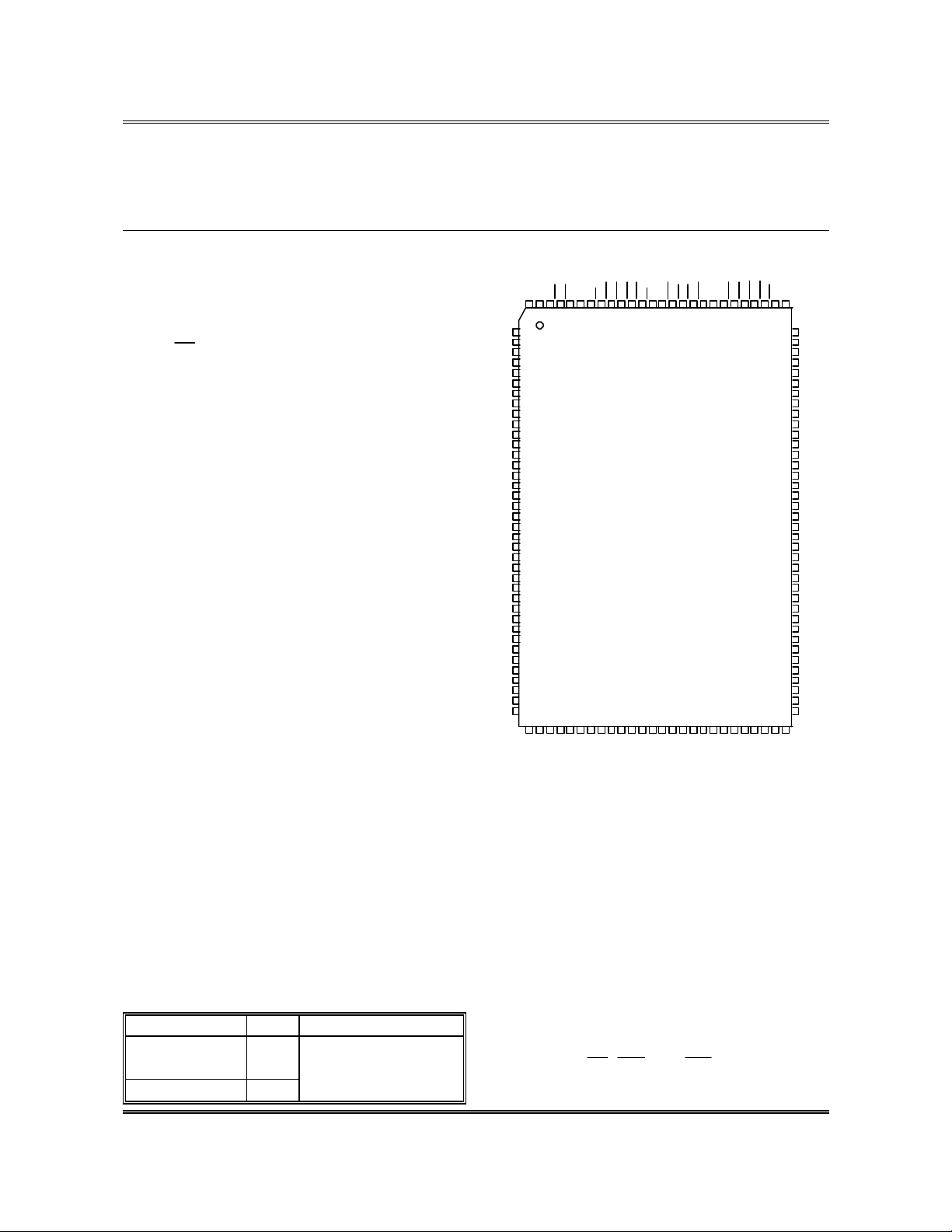
PIN ASSIGNMENT
CE3
VCCQ
CE2
CE3
CE2
123124 116115114113112111110109118119120121122 117128127126125
VSSQ
DQ33
2
DQ34
3
DQ35
4
DQ36
5
DQ37
6
DQ38
7
DQ39
8
DQ40
9
DQ41
10
DQ42
11
DQ43
12
VCCQ
13
VSSQ
14
DQ44
15
DQ45
16
DQ46
17
DQ47
18
DQ48
19
DQ49
20
DQ50
21
DQ51
22
DQ52
23
DQ53
24
VCCQ
25
VSSQ
26
DQ54
27
DQ55
28
DQ56
29
DQ57 DQ8
30
DQ58 31
DQ59 32
DQ60 33
DQ61 34
DQ62 35
DQ63 36
DQ64 37
VCCQ 38
39 49484746454443424140 5756555453525150 58
NC
A14
A15
VSSQ
MODE
BW7
BW8
CE
VCC
VSS
128-pin QFP
128-pin LQFP
A11
A13
A12
VSS
VCC
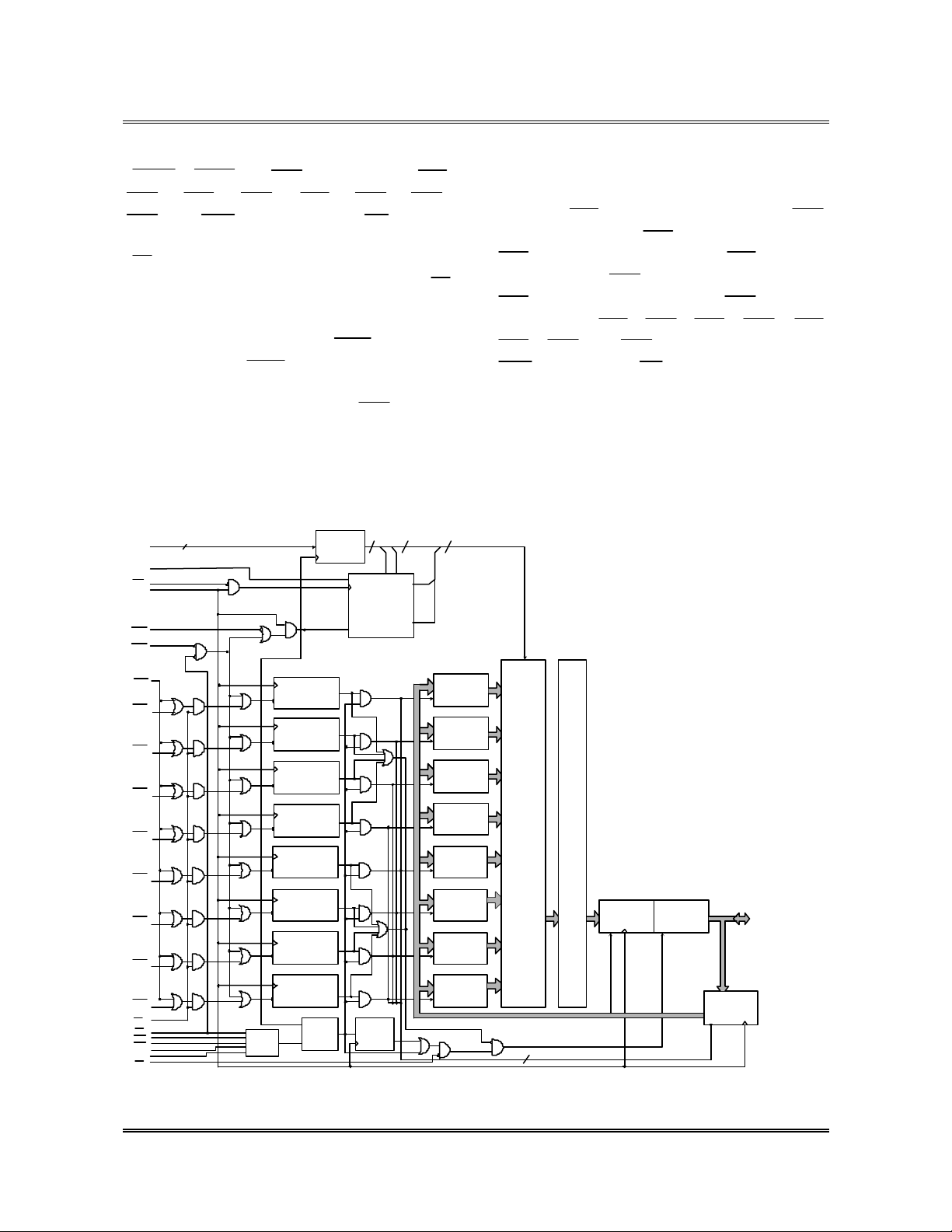
GENERAL DESCRIPTION
The Taiwan Memory Technology Synchronous
Burst RAM family employs: high-speed, low power
CMOS design using advanced triple-layer
polysilicon, double-layer metal technology. Each
memory cell consists of four transistors and two
high valued resistors.
The T35L6464A SRAM integrates 65536 x 64
SRAM cells with advanced synchronous peripheral
circuitry and a 2-bit counter for internal burst
operation. All synchronous inputs are gated by
registers controlled by a positive-edge-triggered
clock input (CLK). The synchronous inputs include
all addresses, all data inputs, three active LOW
chip enable (CE,
chip enables (CE2 and CE3) , burst control inputs
CE2
(Top View)
CLK
OE
BW5
BW6
BWE
or
A9
A8
NC
A10
and
BW3
BW4
GW
VCC
VSS
BW1
BW2
108107106105104103
A3
A4
A5A6A7
VSS
VCC
CE3
), two additional
ADSC
ADSP
6362616059 64
A0A1A2
ADV
ZZ
102
101
100
VSSQ
99
98
97
96
95
94
93
92
91
90
89
88
87
86
85
84
83
82
81
80
79
78
77
76
75
74
73
71
70
69
68
67
66
65
VCCQ
VCCQ1
DQ32
DQ31
DQ30
DQ29
DQ28
DQ27
DQ26
DQ25
DQ24
DQ23
DQ22
VSSQ
VCCQ
DQ21
DQ20
DQ19
DQ18
DQ17
DQ16
DQ15
DQ14
DQ13
DQ12
VSSQ
VCCQ
DQ11
DQ10
DQ9
DQ772
DQ6
DQ5
DQ4
DQ3
DQ2
DQ1
VSSQ
Taiwan Memory Technology, Inc. reserves the right P. 1 Publication Date: AUG. 1998
to change products or specifications without notice. Revision: E
Page 2
TE
C
H
tm
BW8
BWE
BW3
BW1
BW2
BW3
BW4, BW5
T35L6464A
GENERAL DESCRIPTION
ADSC, ADSP
(
BW2, BW3, BW4, BW5, BW6, BW7
and
Asynchronous inputs include the output enable
(OE) , Snooze enable (ZZ) and burst mode control
(MODE). The data outputs (Q), enabled by
are also asynchronous.
Addresses and chip enables are registered with
either address st atus processor (
status controller (
burst addresses can be internally generated as
controlled by the burst advance pin (
Address, data inputs, and write controls are
registered on-chip to initiate self-timed WRITE
cycle. WRITE cycles can be one to eight bytes
wide
ADV
,and
), write enables (
), and global write (GW).
ADSP
) or address
ADSC
) input pins. Subsequent
ADV
).
BW1
OE
FUNCTIONAL BLOCK DIAGRAM
14
A0-A15
MODE
ADV
CLK
ADSC
ADSP
16
ADDRESS
REGISTER
16
A0 A1
DO D1 Q1
BINARY
COUNTER
& LOGIC
LOAD Q0
CLR
A1'
A0'
(continued)
,
,
,
as controlled by the write control inputs.
Individual byte write allows individual byte to be
written.
BW1
controls DQ1-DQ8.
controls DQ9-DQ16.
BW4
controls DQ25-DQ32.
DQ33-DQ40.
BW7
controls DQ49-DQ56.
BW6
DQ57-DQ64.
BW6, BW7
BWE
being LOW.
and
BW8
controls DQ17 -DQ24.
BW5
controls DQ41-DQ48.
BW8
,
,
,
can be active only with
GW
being LOW causes all
BW2
controls
controls
,
bytes to be written. WRITE pass-through
capability allows written data available at the output
for the immediately next READ cycle. This
device also incorporates pipelined enable circuit for
easy depth expansion without penalizing system
performance.
16
8
8
8
8
8
8
8
8
BYTE 8
WRITE DRIVER
BYTE 7
WRITE DRIVER
BYTE 6
WRITE DRIVER
BYTE 5
WRITE DRIVER
BYTE 4
WRITE DRIVER
BYTE 3
WRITE DRIVER
BYTE 2
WRITE DRIVER
BYTE 1
WRITE DRIVER
8
8
8
8
8
8
8
8
64K x 8 x 8
MEMORY
ARRAY
64 64
8
SENSE
AMPS
OUTPUT
REGISTERS
OUTPUT
BUFFERS
64
INPUT
REGISTERS
DQ1
DQ64
.
.
.
BW4
BW3
BW2
BW1
BWE
BW8
BW7
BW6
BW5
GW
CE2
CE3
CE2
CE3
BYTE 8
WRITE REGISTER
BYTE 7
WRITE REGISTER
BYTE 6
WRITE REGISTER
BYTE 5
WRITE REGISTER
BYTE 4
WRITE REGISTER
BYTE 3
WRITE REGISTER
BYTE 2
WRITE REGISTER
BYTE 1
WRITE REGISTER
CE
OE
Chip
Enable
ENABLE
REGISTER
PIPELINED
ENABLE
Note: The Functional Block Diagram illustrates simplified device operation. See Truth Table, pin
descriptions and timing diagrams for detailed information.
Taiwan Memory Technology, Inc. reserves the right P. 2 Publication Date: AUG. 1998
to change products or specifications without notice. Revision: E
Page 3
TE
C
H
tm
BW5
BW6
BW7
GW
ADSP
T35L6464A
PIN DESCRIPTIONS
QFP PINS SYM. TYPE DESCRIPTION
42-44, 47 -51, A0- Input- Addresses: These inputs are registered and must meet the setup and
53-57, 60-62 A15 Synchronous hold times around the rising edge of CLK. The burst counter
107, 108, 111,
112,117 -120 BW8 Synchronous a READ cycle. BW1 controls DQ1-DQ8.
114 BWE Input- Write Enable: This active LOW input gates byte write operations
Synchronous and must meet the setup and hold times around the rising edge of
113
Synchronous to occur independent of the BWE and BWn lines and must meet
the setup and hold times around the rising edge of CLK.
115 CLK Input- Clock: This signal registers the addresses, data, chip enables, write
Synchronous control and burst control inputs on its rising edge. All synchronous
inputs must meet setup and hold times around the clock's rising
121 CE Input- Synchronous Chip Enable: This active LOW input is used to enable
Synchronous the device and conditions internal use of
sampled only when a new external address is loaded.
124 CE2 Input- Synchronous Chip Enable: This active LOW input is used to enable
Synchronous the device. This input is sampled only when a new external address
is loaded. This input can be used for memory depth expansion.
126 CE2 Input- Synchronous Chip Enable: This active HIGH input is used to enable
Synchronous the device. This input is sampled only when a new external address
is loaded. This input can be used for memory depth expansion.
125 CE3 Input- Synchronous Chip Enable: This active LOW input is used to enable
Synchronous the device. This input is sampled only when a new external address
is loaded. This input can be used for memory depth expansion.
127 CE3 Input- Synchronous Chip Enable: This active HIGH input is used to enable
Synchronous the device. This input is sampled only when a new external address
is loaded. This input can be used for memory depth expansion.
116 OE Input Output enable: This active LOW asynchronous input enables the
data output drivers.
BW1
-
Input- Byte Write: A byte write is LOW for a WRITE cyle and HIGH for
Input- Global Write: This active LOW input allows a full 64-bit WRITE
generates internal addresses associated with A0 and A1,during burst
cycle and wait cycle.
BW2 controls DQ9-
DQ16. BW3 controls DQ17 -DQ24. BW4 controls DQ25-DQ32.
controls DQ33 -DQ40.
controls DQ49-DQ56.
high impedance if either of these inputs are LOW ,conditioned by
BWE being LOW.
CLK.
edge.
BW8 controls DQ57 -DQ64. Data I/O are
controls DQ41-DQ48.
. This input is
Taiwan Memory Technology, Inc. reserves the right P. 3 Publication Date: AUG. 199 8
to change products or specifications without notice. Revision: E
Page 4
TE
C
H
tm
ADSP
T35L6464A
PIN DESCRIPTIONS (continued)
QFP PINS SYM. TYPE DESCRIPTION
104 ADV Input- Address Advance: This active LOW input is used to control the
Synchronous internal burst counter. A HIGH on this pin generates wait cycle
(no address advance).
105
Synchronous being LOW, causes a new external address to be registered and a
READ cycle is initiated using the new address.
106 ADSC
Synchronous be de- selected or selected along with new external address to be
write control inputs.
41 MODE
Static selects LINEAR BURST. A NC or HIGH on this pin selects
INTERLEAVED BURST. Do not alter input state while device is
63 ZZ Input Snooze Enable: This active HIGH asynchronous input causes the
device to enter a low -power standby mode in which all data in the
2-12,15-24, DQ1 - Input/ Data Inputs/Outputs: First Byte is DQ1-DQ8. Second Byte is DQ9-
27-37,66-76, DQ64 Output DQ16. Third Byte is DQ17-DQ24. Fourth Byte is DQ25- DQ32.
79-88,91-101 Fifth Byte is DQ 33- DQ40. Sixth Byte is DQ41- DQ48. Seventh
Byte is DQ49- DQ56. Eighth Byte is DQ57- DQ64. Input data
must meet setup and hold times around the rising edge of CLK.
45,58,109,122 VCC Supply Power Supply: 3.3V +10%/-5%.
46,59,110,123 VSS Ground Ground: GND
13,25,38,64, VCCQ I/O Supply Isolated Output Buffer Supply: 3.3V +10%/-5%.
77,89,102,128
1,14,26,39,65,
78,90,103
40,52 NC - No Connect: These signals are not internally conntected.
VSSQ I/O Ground Output Buffer Ground: GND
Input- Address Status Processor: This active LOW input, along withCE
Input- Address Status Controller:This active LOW input causes device to
registered. A READ or WRITE cycle is initiated depending upon
Input- Mode: This input selects the burst sequence. A LOW on this pin
operating.
memory array is retained.
Taiwan Memory Technology, Inc. reserves the right P. 4 Publication Date: AUG. 199 8
to change products or specifications without notice. Revision: E
Page 5
TE
C
H
tm
T35L6464A
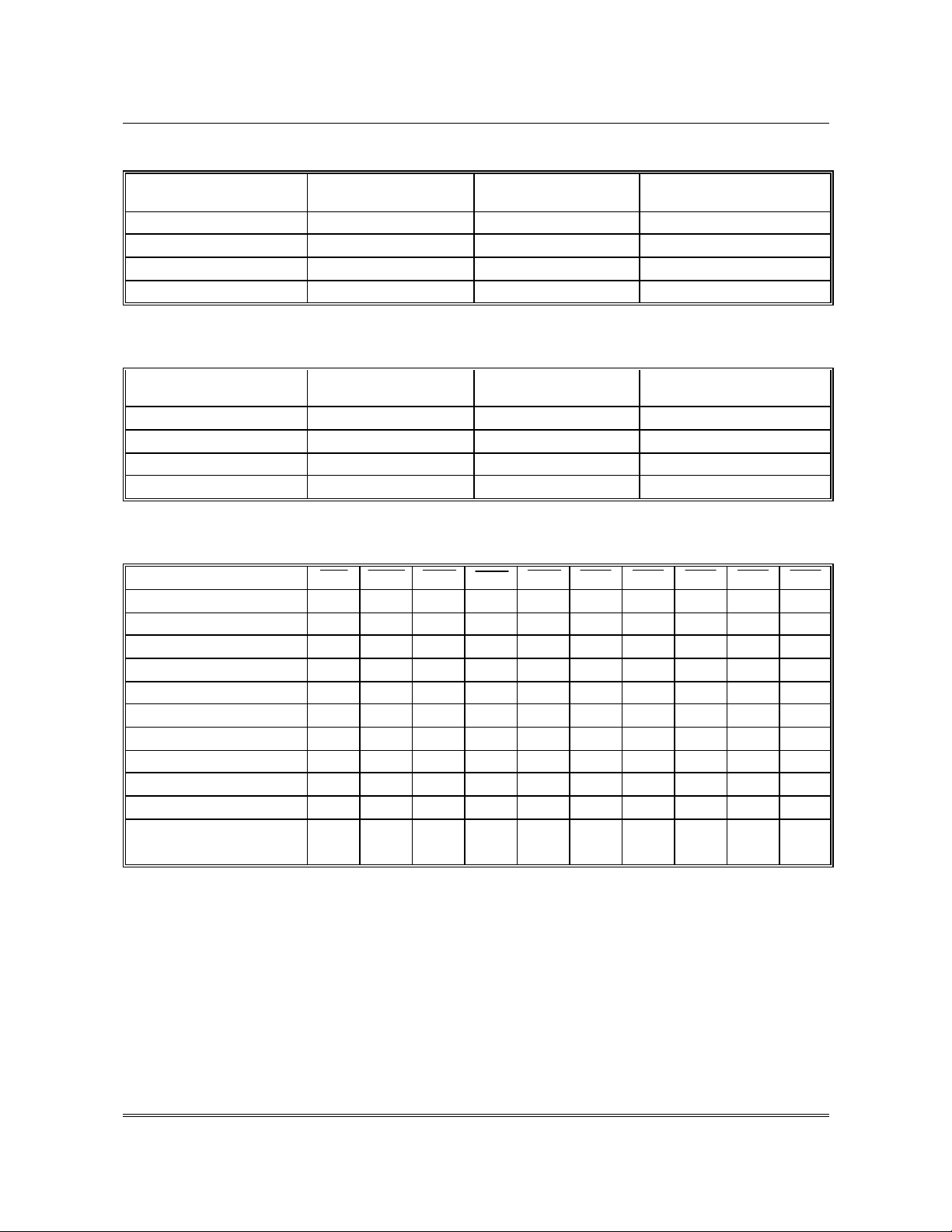
INTERLEAVED BURST ADDRESS TABLE (MODE = NC/Vcc)
First Address
(external)
A...A00 A...A01 A...A10 A...A11
A...A01 A...A00 A...A11 A...A10
A...A10 A...A11 A...A00 A...A01
A...A11 A...A10 A...A01 A...A00
Second Address
(internal)
Third Address
(internal)
Fourth Address
(internal)
LINEAR BURST ADDRESS TABLE (MODE = GND)
First Address
(external)
A...A00 A...A01 A...A10 A...A11
A...A01 A...A10 A...A11 A...A00
A...A10 A...A11 A...A00 A...A01
A...A11 A...A00 A...A01 A...A10
Second Address
(internal)
Third Address
(internal)
Fourth Address
(internal)
PARTIAL TRUTH TABLE FOR READ/WRITE
Function
READ H H X X X X X X X X
READ H L H H H H H H H H
WRITE byte 1 H L L H H H H H H H
WRITE byte 2 H L H L H H H H H H
WRITE byte 3 H L H H L H H H H H
WRITE byte 4 H L H H H L H H H H
WRITE byte 5 H L H H H H L H H H
WRITE byte 6 H L H H H H H L H H
WRITE byte 7 H L H H H H H H L H
WRITE byte 8 H L H H H H H H H L
WRITE all byte H L L L L L L L L L
WRITE all byte L X X X X X X X X X
GW BWE BW1 BW2 BW3
BW4 BW5 BW6 BW7 BW8
Taiwan Memory Technology, Inc. reserves the right P. 5 Publication Date: AUG. 199 8
to change products or specifications without notice. Revision: E
Page 6

TE
C
H
tm
CE2
CE3
CE3 ZZ
WRITE
CLK
WRITE
BW6
BW7
BW8
ADSP
T35L6464A
TRUTH TABLE
OPERATION ADDRESS
Deselected Cycle, Power Down None H X X X X L X L X X X L-H High-Z
Deselected Cycle, Power Down None L X X X L L L X X X X L-H High-Z
Deselected Cycle, Power Down None L X L X X L L X X X X L-H High-Z
Deselected Cycle, Power Down None L X X H X L L X X X X L-H High-Z
Deselected Cycle, Power Down None L H X X X L L X X X X L-H High-Z
Deselected Cycle, Power Down None L X X X L L H L X X X L-H High-Z
Deselected Cycle, Power Down None L X L X X L H L X X X L-H High-Z
Deselected Cycle, Power Down None L X X H X L H L X X X L-H High-Z
De selected Cycle, Power Down None L H X X X L H L X X X L-H High-Z
Snooze Cycle, Power Down None X X X X X H X X X X X X High-Z
READ Cycle, Begin Burst External L L H L H L L X X X L L-H Q
READ Cycle, Begin Burst External L L H L H L L X X X H L-H High-Z
WRITE Cycle, Begin Burst External L L H L H L H L X L X L-H D
READ Cycle, Begin Burst External L L H L H L H L X H L L-H Q
READ Cycle, Begin Burst External L L H L H L H L X H H L-H High-Z
READ Cycle, Continue Burst Next X X X X X L H H L H L L-H Q
READ Cycle, Continue Burst Next X X X X X L H H L H H L-H High-Z
READ Cycle, Continue Burst Next H X X X X L X H L H L L-H Q
READ Cycle, Continue Burst Next H X X X X L X H L H H L-H High-Z
WRITE Cycle, Continue Burst Next X X X X X L H H L L X L-H D
WRITE Cycle, Continue Burst Next H X X X X L X H L L X L-H D
READ Cycle, Suspend Burst Current X X X X X L H H H H L L-H Q
READ Cycle, Suspend Burst Current X X X X X L H H H H H L-H High-Z
READ Cycle, Suspend Burst Current H X X X X L X H H H L L-H Q
READ Cycle, Suspend Burst Current H X X X X L X H H H H L-H High-Z
WRITE Cycle, Suspend Burst Current X X X X X L H H H L X L-H D
WRITE Cycle, Suspend Burst Current H X X X X L X H H L X L-H D
USED
CE
CE2
ADSP ADSC ADV
OE
DQ
Note: 1. X means "don't care." H means logic HIGH. L means logic LOW.
= L means any one
or more byte write enable signals (BW1, BW2 , BW3 , BW4 , BW5 , BW6 , BW7 or BW8 )
and BWE are LOW, or GW equals LOW. WRITE= H means all byte write signal are HIGH.
2. BW1= enables write to DQ1- DQ8. BW2 = enables write to DQ9-DQ16. BW3 = enables write
to DQ17- DQ24. BW4 =enables write to DQ25-DQ32. BW5 = enables write to DQ33-DQ40.
= enables write to DQ41-DQ48.
= enables write to DQ49-DQ56.
= enables
write to DQ57 -DQ64.
3. All inputs except OE must meet setup and hold times around the rising edge ( LOW to HIGH)
of CLK.
4. Suspending burst generates wait cycle.
5. For a write operation following a read operation. OE must be HIGH before the input data
required setup time plus High-Z time for OE and staying HIGH throughout the input data hold
time.
6. This device contains circuitry that will ensure the outputs will be High-Z during power-up.
7.
= LOW along with chip being selected always initiates an internal READ cycle at the L-H
edge of CLK. A WRITE cycle can be performed by setting WRITE LOW for the CLK L-H edge
of the subsequent wait cycle. Refer to WRITE timing diagram for clarification.
Taiwan Memory Technology, Inc. reserves the right P. 6 Publication Date: AUG. 199 8
to change products or specifications without notice. Revision: E
Page 7

TE
C
H
tm
T35L6464A
ABSOLUTE MAXIMUM RATINGS*
Voltage on Vcc Supply Relative to Vss..
………... -0.5V to +4.6V
I/O Supply Voltage VccQ .........…….. -0.5V to Vcc
V
IN (inputs)
Storage Temperature (plastic)...... -55°C to +150°C
Junction Temperature ...........…................ +150°C
Power Dissipation .........................................1.6W
Short Circuit Output Current...................... 100mA
............................ -0.5V to Vcc +0.5V
DC ELECTRICAL CHARACTERISTICS AND RECOMMENDED
OPERATING CONDITIONS
(0°C ≤ TA ≤ 70 °C; Vcc = + 3.3V +10%/-5%; unless otherwise noted)
DESCRIPTION CONDITIONS SYM. MIN MAX UNITS NOTES
Input High (Logic) voltage VIH 2 VccQ + 0.3 V 1, 2
Input Low (Logic) voltage
Input Leakage Current
Output Leakage Current Output(s) disabled, 0V
Output High Voltage IOH = -4.0 mA VOH 2.4 V 1,11
Output Low Voltage IOL = 8.0 mA VOL 0.4 V 1,11
Supply Voltage Vcc 3.1 3.6 V 1
0V ≤ VIN ≤ VCC
≤ V
OUT
≤ VCC
*Stresses greater than those listed under "Absolute
Maximum Ratings" may cause permanent damage
to the device. This is a stress rating only and
functional operation of the device at these or any
other conditions above those indicated in the
operational sections of this specification is not
implied. Exposure to absolute maximum rating
conditions for extended periods may affect
reliability.
VIL -0.3 0.8 V 1, 2
ILI -2 2
ILO -2 2
µA
µA
14
Taiwan Memory Technology, Inc. reserves the right P. 7 Publication Date: AUG. 199 8
to change products or specifications without notice. Revision: E
Page 8

TE
C
H
tm
SYM.
T35L6464A
DC ELECTRICAL CHARACTERISTICS AND RECOMMENDED
OPERATING CONDITIONS
(0°C ≤ TA ≤ 70 °C; Vcc = + 3.3V +10%/-5% unless otherwise noted)
M A
X
DESCRIPTION
Power Supply Device selected; all inputs Icc 200 300 260 240 210 mA 3, 12, 13
Current:
Operating
Power Supply Dev ice selected;ADSC ,
Current: Idle ADSP,ADV,GW, BWE
CMOS Standby Device deselected; VCC =
MAX; all inputs ≤ VSS + 0.2
or ≥ VCC - 0.2; all inputs
TTL Standby Device deselected; all inputs ISB3 15 40 40 40 40 mA 12, 13
CLK frequency = 0
Clock Running Device deselected; all inputs ≤ ISB4 30 81 76 66 51 mA 12, 13
CONDITIONS
≤V
or ≥ VIH; cycle time
IL
≥tKC MIN; VCC = MAX;
outputs open
≥ VIH; all other inputs ≤ VIL
or ≥VIH; VCC = MAX; cycle
time ≥tKC MIN: outputs open
static; CLK frequency = 0
≤ VIL or ≥ VIH; all inputs
static; VCC = MAX;
VIL or ≥ VIH; VCC = MAX;
CLK cycle time ≥ tKCMIN
TYP -5 -6 -7 -8 UNITS NOTES
I
SB1 30 60 55 50 45 mA 12, 13
I
SB2 2 10 10 10 10 mA 12, 13
CAPACITANCE
DESCRIPTION CONDITIONS SYM. TYP MAX UNITS NOTES
Input Capacitance
Input/ Output
Capacitance(DQ)
TA = 25°C; f = 1 MHz CI
VCC = 3.3V
CO
3 4 pF 4
6 7 pF 4
THERMAL CONSIDERATION
DESCRIPTION CONDITIONS SYM. QFP TYP UNITS NOTES
Thermal Resistance - Junction to
Ambient
Thermal Resistance - Junction to
Case
Taiwan Memory Technology, Inc. reserves the right P. 8 Publication Date: AUG. 199 8
to change products or specifications without notice. Revision: E
Still air, soldered on
4.25x
1.125 inch 4-layer PCB
ΘJA
ΘJB
20 °C/W
1 °C/W
Page 9

TE
C
H
tm
BW8
T35L6464A
AC ELECTRICAL CHARACTERISTICS
(Note 5) (0 °C ≤ TA ≤ 70 °C; Vcc = + 3.3V +10%/-5%)
DESCRIPTION -5 -6 -7 -8
SYM. MIN
Clock
Clock cycle time
Clock HIGH time
Clock LOW time
Output Times
Clock to output valid
Clock to output invalid
Clock to output in Low-Z tKQLZ 4 5 5 5 ns 6,7
Clock to output in High-Z tKQHZ 5 5 6 6 ns 6,7
OE to output valid
OE to output in Low -Z
OE to output in High-Z
Setup Times
Address
Address Status
( ADSC , ADSP )
Address Advance ( ADV ) tAAS 3 3 3 3 ns 8,10
Byte Write Enables
(BW1~BW8 ,BWE,GW)
Data -in
Chip Enables (CE ,
CE2,CE2,CE3,CE3)
Hold Times
Address
Address Status
( ADSC , ADSP )
Address Advance ( ADV ) tAAH 0.5 0.5 0.5 0.5 ns 8,10
Byte Write Enables
(BW1~
Data -in
Chip Enables (CE,
CE2,CE2, CE3,CE3)
,BWE,GW)
t
KC 10 12 15 20 ns
t
KH 4 4.5 5 6 ns
t
KL 4 4.5 5 6 ns
t
KQ 5 6 7 8 ns
t
KQX 2 2 2 2 ns
t
OEQ 5 5 5 6 ns 9
t
OELZ 0 0 0 0 ns 6,7
t
OEHZ 4 5 6 6 ns 6,7
t
AS 3 3 3 3 ns 8,10
t
ADSS 3 3 3 3 ns 8,10
t
WS 3 3 3 3 ns 8,10
t
DS 3 3 3 3 ns 8,10
t
CES 3 3 3 3 ns 8,10
t
AH 0.5 0.5 0.5 0.5 ns 8,10
t
ADSH 0.5 0.5 0.5 0.5 ns 8,10
t
WH 0.5 0.5 0.5 0.5 ns 8,10
t
DH 0.5 0.5 0.5 0.5 ns 8,10
t
CEH
MAX MIN MAX MIN MAX MIN MAX UNITS NOTES
0.5 0.5 0.5 0.5 ns
8,10
Taiwan Memory Technology, Inc. reserves the right P. 9 Publication Date: AUG. 199 8
to change products or specifications without notice. Revision: E
Page 10

TE
C
H
tm
ADSC
ADV
ADSP
T35L6464A
AC TEST CONDITIONS
Input pulse levels 0V to 3.0V
Input rise and fall times 1.5ns
Input timing reference
levels
Output reference levels 1.5V
Output load See Figures 1 and 2
Notes:
1. All voltages referenced to Vss (GND).
2. Overshoot: VIH ≤ +3.6 V for t ≤ tKC/2
Undershoot: VIL ≥ -1.0 V for t ≤ tKC/2
3. Icc is given with no output current. Icc increases
with greater output loading and faster cycle
times.
4. This parameter is sampled.
5. Test conditions as specified with the output
loading as shown in Fig. 1 unless otherwise
noted.
6. Output loading is specified with CL=5 pF as in
Fig.2.
7. At any given temperature and voltage condition,
t
KQHZ is less than tKQLZ and tOEHZ is less
than tOELZ.
1.5V
OUTPUT LOADS
8. A Write cycle is defined by at least one byte
write enable LOW and ADSP HIGH for the
required setup and hold times. A Read cycle
is defined by all byte write enables HIGH and
(
the required setup and hold times.
9. OE is a "don't care" when a byte write enable is
sampled LOW.
10.This is a synchronous device. All synchronous
inputs must meet the setup and hold times,
except for “don‘t care” as defined in the truth
table.
11.AC I/O curves are available upon request.
12."Device Deselected means the device is in
POWER- DOWN mode as defined in the truth
table. "Device Selected" means the device is
active.(not in POWER-DOWN mode).
13.Typical values are measured at 3.3V 25°C and
20ns cycle time.
14.MODE pin has an internal pull -up and exhibits
an input leakage current of ± 10µA.
or
LOW) or
LOW for
DQ
50
Z0 = 50
Fig.1 OUTPUT LOAD EQUIVALENT
DQ
351
Fig.2 OUTPUT LOAD EQUIVALENT
Taiwan Memory Technology, Inc. reserves the right P. 10 Publication Date: AUG. 1998
to change products or specifications without notice. Revision: E
Vt =1.5V
3.3V
30 pF
317
5 pF
Page 11

TE
C
H
tm
CE
T35L6464A
SNOOZE MODE
SNOOZE MODE is a low current, “power
down” mode in which the device is deselected and
the current is reduced to I
The duration of
ZZ.
SNOOZE MODE is dictated by the length of time
the ZZ pin is in a HIGH state. After entering
SNOOZE MODE, the clock and all other inputs
are ignored.
The ZZ pin (pin 63) is an asynchronous ,
active HIGH input that causes the device to enter
SNOOZE MODE. When the ZZ pin becomes a
logic HIGH, I
t
ZZ is met. Any access pending when entering
is guaranteed after the setup time
ZZ
SNOOZE MODE is not guaranteed to successfully
complete. Therefore, SNOOZE MODE must not
be initiated until valid pending operations are
completed.
SNOOZE MODE ELECTRICAL CHARACTERISTICS
DESCRIPTION CONDITIONS SYMBOL MIN MAX UNITS NOTES
Current during
ZZ ≥ VIH IZZ 10 mA
SNOOZE MODE
ZZ HIGH to
t
ZZ 2(tKC) ns 3
SNOOZE MODE time
SNOOZE MODE
t
RZZ 2(tKC) ns 3
Operation Recovery Time
SNOOZE MODE WAVEFORM
C L K
C E
t
RZZ
Z Z
t
ZZ
I
SUPP LY
Note: 1. The
signal shown above refers to a TRUE state on all chip selects for the device.
2. All other inputs held to static CMOS levels (VIN ≤ Vss + 0.2 V or ≥ Vcc -0.2 V).
3. This parameter is sampled.
I
ZZ
DON'T CA RE
I
SU PP L Y
Taiwan Memory Technology, Inc. reserves the right P. 11 Publication Date: AUG. 1998
to change products or specifications without notice. Revision: E
Page 12

TE
C
H
tm
t
CE2
CE3
CE
CE2
CE3
T35L6464A
READ TIMING
C L K
t
AD SSt ADSH
A D S P
A D S C
t ASt
t
K Ht KL
A H
KC
t
A DSSt ADSH
A D D R E S S
G W , B W E ,
B W 1 - B W 8
C E
( N O T E 2 )
A D V
O E
t WSt
WH
t
C ESt CEH
t
AASt AA H
ADV susp en d s bu rs t .
t
(NOTE3)
t
K QLZ
Q
Hig h -Z
t
KQ
Sing le R E A D
t
OEHZ
Q(A1) Q (A 2) Q (A2+1) Q(A2+2 ) Q (A2+3) Q (A 2+1)
OEQ
t
OELZ
t
t
KQX
(NOTE1)
KQ
BUR ST READ
A 3A 2A1
Burst continue d w ith
new ba s e ad d re ss .
t
Q(A2)
Burst wr ap s ar ou nd
to its inita l s ta te .
Deselect cycle.
(NOTE4)
KQHZ
D O N 'T CA R E
U ND E FI N E D
Note: 1. Q(A2) refers to output from address A2. Q (A2 + 1) refers to output from the next internal burst
address following A2.
2. CE2 , CE2, CE3and CE3 have timing identical to CE . On this diagram, when CE is LOW,
,
is LOW and CE2 , CE3 is HIGH. When
is HIGH,
,
is HIGH and
CE2 , CE3 is LOW.
3. Timing is shown assuming that the device was not enabled before entering into this sequence. OE
does not cause Q to be driven until after the following clock rising edge.
4. Outputs are disabled within one clock cycle after deselect.
Taiwan Memory Technology, Inc. reserves the right P. 12 Publication Date: AUG. 1998
to change products or specifications without notice. Revision: E
Page 13

TE
C
H
tm
t
GW
GW
BWE
BW1
BW8
T35L6464A
WRITE TIMING
C L K
t
AD S St AD SH
t KHt
K C
K L
A D S P
A D S C
A D D R E S S
B W E ,
B W 1 - B W 8
G W
C E
( N O T E 2 )
A D V
O E
t
AD S St AD SH
t ASt
AH
BYTE W RITE s ig na ls ar e
ig no red f or fir s t c y c le wh en
AD S P init ia lt es b u r s t.
t
C ESt CEH
(NOTE3)
t DSt
ADSC exte nd s b ur s t .
t WSt
WH
(NOTE5)
ADV susp nd s b u rs t .(NOTE4)
DH
t
AD SSt AD SH
A 3A2A1
t WSt
t
AA St AAH
WH
H ig h-Z
D
Q
BU R S T R E A D Exte nd e d B U R S T W R IT E
D(A1) D(A2) D(A2+1) D(A2+2) D(A2+3) D(A3+1)D(A3)
t
OEHZ
Sing le W R IT E
(NOTE1)
D(A2+1) D(A3+2)
BU R S T W R ITE
DON 'T CA R E
UND E F IN E D
Note: 1. Q(A2) refers to output from address A2. Q (A2 + 1) refers to output from the next internal burst address
following A2.
2. CE2, CE2, CE3 and CE3 have timing identical to CE . On this diagram, when CE is LOW, CE2,
CE3 is LOW and CE2, CE3 is HIGH. When CE is HIGH, CE2, CE3 is HIGH and CE2, CE3 is
LOW.
3. OE must be HIGH before the input data setup and hold HIGH throughout the data hold time. This prevents
input/output data contention for the time period to the byte write enable inputs being sampled.
4. ADV must be HIGH to permit a WRITE to th e loaded address.
5. Full width WRITE can be initiated by
LOW or
HIGH and
,
-
LOW.
Taiwan Memory Technology, Inc. reserves the right P. 13 Publication Date: AUG. 1998
to change products or specifications without notice. Revision: E
Page 14

TE
C
H
tm
t
T35L6464A
READ/WRITE TIMING
C L K
t
A DSSt A DSH
A D S P
A D S C
t ASt
t KHt
AH
KC
KL
A D D R E S S
B W 1 - B W 8
C E
( N O T E 2 )
A D V
O E
A 2 A6
t WSt
t
C ESt C EH
t
OEHZ
t
DS
Si ng le W R ITE
t
KQ
D
Q
Hig h-Z D(A3) D (A5) D (A6)
t
KQLZ
Hig h-Z
Q(A1 ) Q(A2) Q(A3 ) Q (A4) Q(A4+1
Back-to-Bac k READs P as s -throu gh
A 4
WH
t
DH
t
OELZ
t
K Q
READ
(NOTE1)
)
BU R S T R E A D
Q(A4+3 )Q(A4+2)
A5A 3A1
Bac k-to-Back
DO N' T CARE
UN DE F I NE D
WRITEs
Note: 1. Q (A4) refers to output from address A4. Q (A4 + 1) refers to output from the next internal burst
address following A4.
2. CE2, CE2, CE3 and CE3 have timing identical to CE . On this diagram, when CE is LOW,
CE2, CE3 is LOW and CE2, CE3 is HIGH. When CE is HIGH, CE2, CE3 is HIGH and CE2,
CE3 is LOW.
3. The data bus (Q) remains in High-Z following a WRITE cycle unless an ADSP , ADSC or
ADV cycle is performed.
4. GW is HIGH.
5. Back -to-back READs may be controlled by either ADSP or ADSC.
Taiwan Memory Technology, Inc. reserves the right P. 14 Publication Date: AUG. 1998
to change products or specifications without notice. Revision: E
Page 15

TE
C
H
tm
T35L6464A
PACKAGE DIMENSIONS
128 -LEAD QFP SSRAM (14 x 20 mm)
Seating Plane y
SYMBOL DIMENSIONS IN INCHES DIMENTION IN MM
A 0.134(MAX) 3.400(MAX)
A1 0.107+0.007-0.009 2.720+0.180-0.220
A2 0.010(MIN) 0.250(MIN)
b 0.008+0.00 3-0.001 0.200+0.070-0.030
D 0.551 14.000
E 0.787 20.000
e 0.020 0.500
HD' 0.677 17.200
HE' 0.913 23.200
L' 0.035±0.006 0.880± 0.150
L1' 0.063±0.006 1.600±0.150
t 0.006+0.003-0.002 0.150+0.080-0.040
y 0.003 0.0 80
θ 0°~7° 0°~7°
Taiwan Memory Technology, Inc. reserves the right P.15 Publication Date: AUG. 1998
to change products or specifications without notice. Revision: E
Page 16

TE
C
H
tm
T35L6464A
PACKAGE DIMENSIONS
128 -LEAD LQFP SSRAM (14 x 20 mm)
Seating Plane y
SYMBOL DIMENSIONS IN INCHES DIMENTION IN MM
A 0.063(MAX) 1.600(MAX)
A1 0.055±0.002 1.400±0.050
A2 0.002(MIN) 0.050(MIN)
b 0.008+0.003 -0.001 0.200+0.070-0.030
D 0.551 14.000
E 0.787 20.000
e 0.020 0.500
HD' 0.630 16.000
HE' 0.866 22.000
L' 0.024±0.006 0.600± 0.150
L1' 0.039 1.000
t 0.004(MIN),0.008(MAX) 0.090(MIN),0.200(MAX)
y 0.003 0.0 80
θ 0°~7° 0°~7°
Taiwan Memory Technology, Inc. reserves the right P.16 Publication Date: AUG. 1998
to change products or specifications without notice. Revision: E
 Loading...