

Page 1
FEATURES
HIGHCOMMUTATION (dI/dt)c> 11 A/ms
withoutsnubber
HIGHSTATICdV/dt > 500V/µs
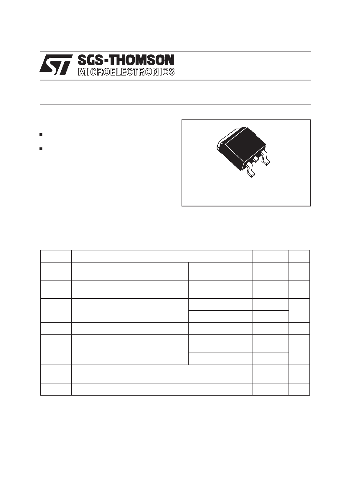
T2035-600G
HIGH PERFORMANCE TRIAC
A2
DESCRIPTION
The T2035-600G triac uses a high performance
SNUBBERLESS
TM
technology.
The part is intended for general purpose
applicationsusingsurfacemounttechnology.
D
2
PAK
A1
A2
G
ABSOLUTERATINGS (limitingvalues)
Symbol Parameter Value Unit
V
DRM
V
RRM
I
T(RMS)
Repetitivepeak off-statevoltage
RMSon-statecurrent
Tj= 125°C 600 V
Tc=100°C20A
(360°conduction angle)
I
TSM
Non repetitivesurgepeak on-statecurrent
tp = 8.3ms 210 A
(Tj initial= 25°C)
tp = 10ms 200
2
tI
I
2
t Value(half-cycle,50 Hz) tp = 10ms 200 A2s
dI/dt Criticalrate of riseof on-statecurrent
Repetitive
F = 50Hz
I
=500 mA dIG/dt =1 A/µs.
G
Non Repetitive 100
T
stg
T
j
Storagetemperaturerange
Operatingjunctiontemperaturerange
Tl Maximumtemperaturefor solderingduring 10s 260
January 1998- Ed: 1D
20 A/µs
-40, +150
-40, +125
°C
°
C
1/5
Page 2
T2035-600G
THERMALRESISTANCES
Symbol Parameter Value Unit
2
Rth(j-a) Junctionto ambiant(S=1cm
Rth(j-c) Junctionto casefor DC 1.5 °C/W
)45°C/W
Rth(j-c)
GATECHARACTERISTICS
P
=1W PGM= 10W (tp = 20µs) IGM=4A(tp=20µs)
G (AV)
Junctionto caseforAC 360°conductionangle(F=50Hz)
(maximumvalues)
1.1
ELECTRICALCHARACTERISTICS
Symbol Test Conditions Quadrant Sensitivity Unit
I
GT
VD=12V (DC) RL=33
Ω
Tj= 25°C I-II-III MIN 2 mA
MAX 35
V
GT
V
GD
*I
I
H
I
L
V
TM*
I
DRM
I
RRM
VD=12V (DC) RL=33Ω
VD=V
DRMRL
= 500mA Gateopen Tj= 25°C MAX 35 mA
T
IG=1.2 I
=3.3kΩ Tj= 125°C I-II-III MIN 0.2 V
GT
Tj= 25°C I-II-III MAX 1.3 V
Tj= 25°C I-II-III MAX 80 mA
ITM= 28A tp= 380µs Tj= 25°C MAX 1.5 V
VD=V
VR=V
DRM
RRM
Tj= 25°C MAX 5
Tj=125°C MAX 2 mA
°
C/W
µ
A
dV/dt* Linearslope uptoV
=67%V
D
DRM
Tj= 125°C MIN 500 V/µs
Gateopen
(dI/dt)c* Withoutsnubber Tj= 125°C MIN 11 A/ms
* For eitherpolarity of electrode A2 voltagewith referenceto electrode A1.
ORDERINGINFORMATION
Add”-TR” suffixfor Tape &Reelshipment
T 20 35 - 600 G
PACKAGE:
2
G=D
VOLTAGE
PAK
2/5
TRIAC
CURRENT
SENSITIVITY
Page 3

T2035-600G
Fig. 1:
Maximum power dissipation versus RMS
on-statecurrent.
P(W)
25
20
15
10
α=90°
α=60°
α=30°
5
α=180°
α=120°
I (A)T(RMS)
0
0 5 10 15 20
Fig. 3:
RMS on-state current versus case tem-
perature.
I (A)
T(RMS)
22
20
18
16
14
12
10
8
6
4
2
0
0 25 50 75 100 125
α=180°
Tcase(°C)
Fig.2:
Correlationbetweenmaximumpowerdissipation and maximum allowable temperatures
(T
amb
and T
) for different thermal resistances
case
heatsink+contact.
P(W) Tcase (°C)
25
Rth=4°C/W
20
15
10
5
0
0 20 40 60 80 100 120 140
Fig. 4:
α=180°
Tamb(°C)
Relative variation of thermal impedance
Rth=0°C/WRth=1°C/WRth=2°C/W
100
105
110
115
120
125
versuspulseduration.
K=[Zth/Rth]
1.00
Zth(j-c)
Zth(j-a)
0.10
tp(s)
0.01
1E-3 1E-2 1E-1 1E+0 1E+1 1E+2 5E+2
Fig.5:
Relativevariationof gatetriggercurrentand
holding current versus junction temperature(typicalvalues).
I ,I [Tj]/I ,I [Tj=25°C]GT H GT H
2.5
2.0
1.5
1.0
0.5
0.0
IGT
IH
Tj(°C)
-40 -20 0 20 40 60 80 100 120 140
Fig. 6:
Non repetitive surge peak on-statecurrent
versusnumberof cycles.
I (A)TSM
200
180
160
140
120
100
80
60
40
20
0
1 10 100 1000
Number of cycles
Tj initial=25°C
F=50Hz
3/5
Page 4

T2035-600G
Fig. 7: Non repetitive surge peak on-state current
fora sinusoidalpulsewith widthtp<10ms,and correspondingvalue of I
I
(A),I t(A s)
TSM
1000
500
200
100
12 510
Fig.9:
Thermalresistancejunctiontoambientver-
2
I t
t.
Tj initial=25°C
ITSM
tp(ms)
suscoppersurfaceundertab (Epoxy printed circuit
boardFR4, copperthickness:35µm).
Rth(j-a) (°C/W)
80
70
60
50
40
30
20
10
0
0 4 8 12 16 20 24 28 32 36 40
S(Cu) (cm )
Fig.8:On-statecharacteristics(maximumvalues).
TM
I (A)
200
Tj max.:
Vto=0.87V
100
Rt=20 mΩ
Tj=Tj max.
10
Tj=25°C
V (V)TM
1
0.0 0.5 1.0 1.5 2.0 2.5 3.0 3.5 4.0 4.5 5.0
Fig.10:
Typicalreflow solderingheatprofile,either
formounting onFR4 or metal-backedboards.
T(°C)
250
200
150
100
50
0
0 40 80 120 160 200 240 280 320 360
Epoxy FR4
board
Metal-backed
245°C
215°C
board
t (s)
4/5
Page 5

PACKAGEMECHANICALDATA
2
D
PAK
L2
L
L3
Note 1: Max resin gateprotusion = 0.5 mm
E
A1
B2
B
G
2.0 MIN.
FLATZONE
C2
T2035-600G
DIMENSIONS
REF.
A
A 4.30 4.60 0.169 0.181
A1 2.49 2.69 0.098 0.106
A2 0.03 0.23 0.001 0.009
D
B 0.70 0.93 0.027 0.037
B2 1.40 0.055
C 0.45 0.60 0.017 0.024
C
R
C2 1.21 1.36 0.047 0.054
D 8.95 9.35 0.352 0.368
E 10.00 10.28 0.393 0.405
A2
G 4.88 5.28 0.192 0.208
L 15.00 15.85 0.590 0.624
L2 1.27 1.40 0.050 0.055
V2
L3 1.40 1.75 0.055 0.069
R 0.40 0.016
V2 0° 8° 0° 8°
Millimeters Inches
Min. Typ. Max. Min. Typ. Max.
FOOTPRINT DIMENSIONS
16.90
(in millimeters)
MARKING
: T2035
600G
10.30
8.90
Information furnished is believed to be accurate and reliable. However, SGS-THOMSON Microelectronics assumes no responsibility for the
consequences of use of such information nor forany infringementof patents or other rights ofthird parties which mayresult from its use.No
license is grantedby implication or otherwise underany patent orpatent rights of SGS-THOMSON Microelectronics.Specificationsmentioned
in this publicationare subject tochange withoutnotice. This publicationsupersedes andreplaces all information previously supplied.
SGS-THOMSONMicroelectronics productsarenot authorizedfor use as critical components in lifesupport devicesor systemswithout express
written approval ofSGS-THOMSON Microelectronics.
3.70
1998 SGS-THOMSON Microelectronics- Printed in Italy- All rights reserved.
SGS-THOMSON Microelectronics GROUP OF COMPANIES
Australia -Brazil - Canada - China -France - Germany -Italy - Japan - Korea- Malaysia - Malta - Morocco
The Netherlands- Singapore - Spain - Sweden- Switzerland - Taiwan - Thailand - United Kingdom -U.S.A.
5.08
1.30
5/5
 Loading...