

Datasheet T15N1M16A-70CI, T15N1M16A-70C, T15N1M16A-70S, T15N1M16A-70SI, T15N1M16A-70JI Datasheet (Taiwan Memory Technology)
...Page 1
TE
tm
SRAM
CH
T15N1M16A
FEATURES
• Fast access time : 55/70/100 ns
• Single +2.4 to 3.6V Power Supply
• Low power supply current :
- Operating :30mA(max)
- Standby : 10uA
• TTL compatible , Tri-state output
• Common I/O capability
• Automatic power-down when deselected
• Full static operation, no clock or refresh required
• Available packages type :
- 44-PIN SOJ (400 mil)
- 44-PIN TSOP-II (400 mil)
- 48-PIN CSP
64K X 16 LOW POWER
CMOS STATIC RAM
GENERAL DESCRIPTION
The T15N1M16A is a low power CMOS Static
RAM organized as 65,536 words by 16 bits. That
operates on a wide voltage range from +2.4 to 3.6V
power supply, Fabricated using high performance
CMOS technology, Inputs and three-state outputs
are TTL compatible and allow for direct interfacing
with common system bus structures. Data retention
is guaranteed at a power supply voltage as low as
1.5V.
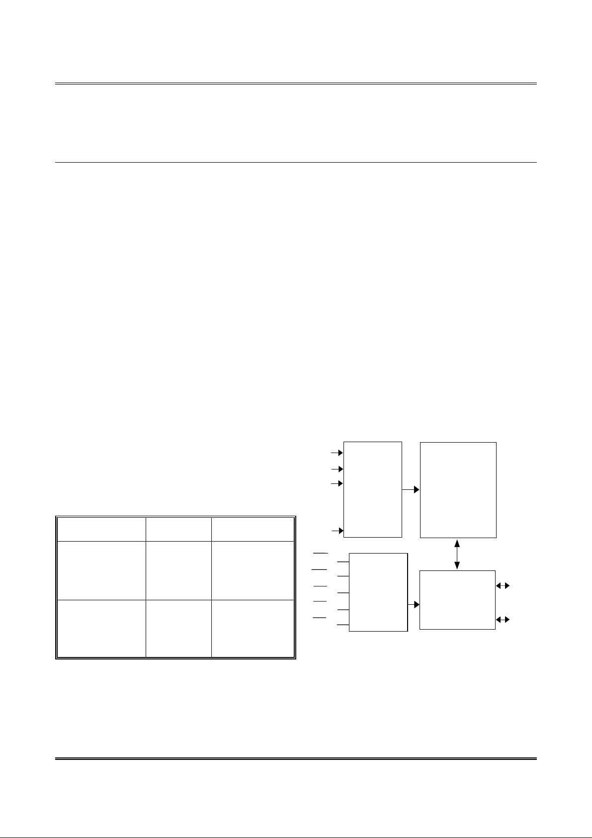
BLOCK DIAGRAM
Operating temperature :
•
- 0 ~ +70 °C
- -40 ~ +85 °C
PART NUMBER EXAMPLES
PART NO.
T15N1M16A-70J
T15N1M16A-70S
T15N1M16A-70C
T15N1M16A-70JI
T15N1M16A-70SI
T15N1M16A-70CI
PACKAGE
CODE
J=SOJ
S=TSOP-II
C= CSP
J=SOJ
S=TSOP-II
C= CSP
Operating
Temperature
0 ~ +70 °C
-40 ~ +85 °C
Vcc
Vss
A0
A15
CE
WE
OE
LB
UB
.
.
DECODER
CONTROL
CIRCUIT
CORE
ARRAY
DATA I/O
I/O 1
.
.
.
I/O 1 6
TM Technology Inc. reserves the right P. 1 Publication Date: JUL . 2002
to change products or specifications without notice. Revision: A
Page 2
TE
A4
A3
A2
A1
A0
CE
I/O1
I/O2
I/O3
I/O4
VCC
VSS
I/O5
I/O6
I/O7
I/O8
WE
A15
A14
A13
A12
NC
CH
T15N1M16A
1
2
3
4
5
6
7
8
9
10
11
12
13
14
15
16
17
18
19
20
21
22
SOJ
&
TSOP-II
tm
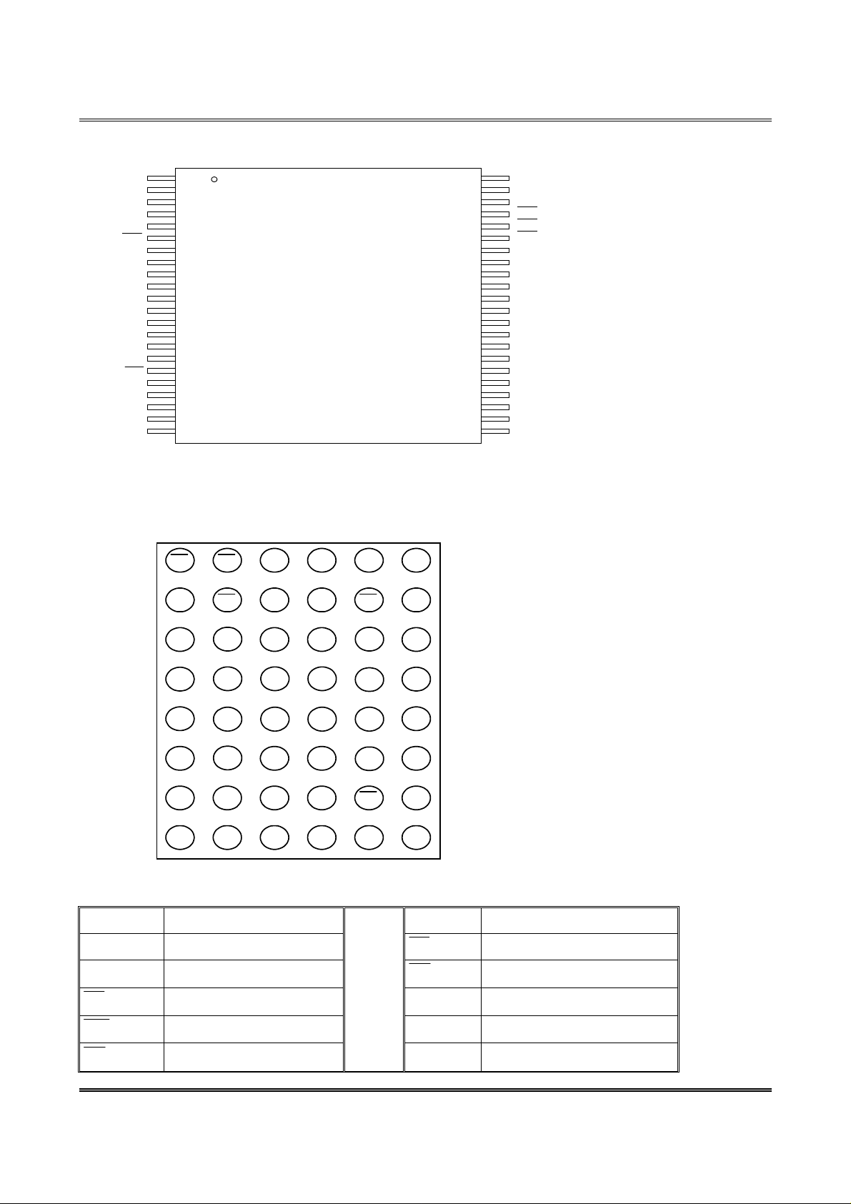
PIN CONFIGURATIONS
48-Ball CSP TOP VIEW (Ball Down)
44
43
42
41
40
39
38
37
36
35
34
33
32
31
30
29
28
27
26
25
24
23
A5
A6
A7
OE
UB
LB
I/O16
I/O15
I/O14
I/O13
VSS
VCC
I/O12
I/O11
I/O10
I/O9
NC
A8
A9
A10
A11
NC
654321
A
B
C
D
E
F
G
H
LB OE
I/O 9
I/O 10
VSS
VCC
I/O 15
I/O 16
NC A8
UB
I/O 11
I/O 12
I/O 13
I/O 14
NC
A0 A1 A2
A5
NC
NC
A14
A12 A13
A9 A10
A6
A7
NC
A15
CEA4A3
I/O 2
I/O 4
I/O 5
I/O 6
WE
A11 NC
NC
I/O 1
I/O 3
VCC
VSS
I/O 7
I/O 8
PIN DESCRIPTIONS
SYMBOL DESCRIPTIONS SYMBOL DESCRIPTIONS
A0 ~ A15 Address inputs
I/O1~I/O16 Data inputs/outputs
LB
UB
Lower byte (I/O 1~8)
Upper byte (I/O 9~16)
CE
WE
OE
TM Technology Inc. reserves the right P. 2 Publication Date: JUL . 2002
to change products or specifications without notice. Revision: A
Chip enable VCC Power supply
Write enable input VSS Ground
Output enable input
NC No connection
Page 3
TE
tm
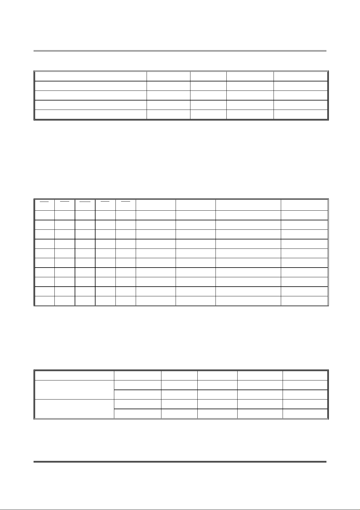
ABSOLUTE MAXIMUM RATINGS*
Voltage on Any Pin Relative to VSS VR -0.5 +4.6 V V
Power Dissipation
Storage Temperature
Temperature Under Bias
*Note: Stresses greater than those listed above Absolute Maximum Ratings may cause permanent damage to
TRUTH TABLE
CH
T15N1M16A
PARAMETER SYM MIN. MAX. UNIT
P
D
T
STG
I
BIAS
the device. This is a stress rating only and function operation of the device at these or any other
conditions outside those indicated in the operational sections of this specification is not implied.
Exposure to absolute maximum rating conditions for extended periods may affect reliability.
- 0.7 W
-55 +150 °C
0 / -40 +70 / +85 °C
CE
H X* X* X* X* High-Z High-Z Deselected
X* X* X* H H High-Z High-Z Deselected
*Note: X = Don’t Care (Must be low or high state), L = Low, H = High
OE WE
L H H L X* High-Z High-Z Output Disabled Active
L H H X* L High-Z High-Z Output Disabled Active
L L H L H Data Out High-Z Lower Byte Read Active
L L H H L High-Z Data Out Upper Byte Read Active
L L H L L Data Out Data Out Word Read Active
L X* L L H Data In High-Z Lower Byte Write Active
L X* L H L High-Z Data In Upper Byte Write Active
L X* L L L Data In Data In Word Write Active
LB
UB
I/O 1~8 I/O 9~16 MODE Power
Standby
Standby
RECOMMENDED OPERATING CONDITIONS
(Ta = 0°C to +70°C / -40 °C ~ +85 °C *)
PARAMETER SYM MIN TYP MAX UNIT
Supply Voltage
Input Voltage
V
*
min = -1.0V for pulse width less than
IL
Vcc 2.4 - 3.6 V
V
V
V
SS
IH
IL
0.0 0.0 0.0 V
2.0 - Vcc+0.3 V
-0.5* - 0.4 V
/2
t
RC
TM Technology Inc. reserves the right P. 3 Publication Date: JUL . 2002
to change products or specifications without notice. Revision: A
Page 4
TE
tm
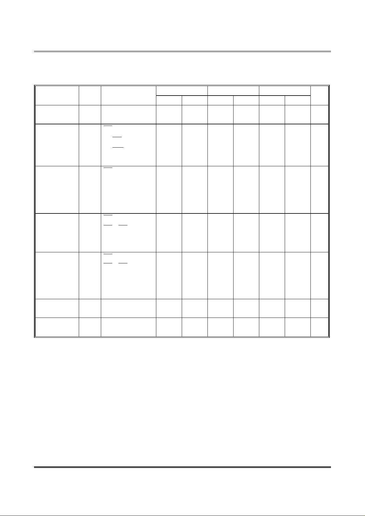
OPERATING CHARACTERISTICS
CH
T15N1M16A
(Vcc =
PARAMETER SYM. TEST CONDITIONS
Output Leakage
Operating Power
+2.4 to 3.6V , V
Input Leakage
Current
Current
Supply Current
ILI
ILO
ICC
= 0V, Ta = 0°C to +70°C / -40°C to +85 °C)
SS
Vcc = Max,
VIN = V
CE
or
or
V
IO
CE
VIN
I
OUT
to Vcc
SS
= VIH
= VIH
OE
= VIL
WE
= V
to Vcc
SS
= VIL,
= VIH or V
=0mA
IL,
Cycle time=min,
Standby Power
Supply Current
(TTL Level)
Standby Power
Supply Current
(CMOS Level)
Output Low
Voltage
Output High
Voltage
V
V
100% duty
CE
LB
I
SB
other input= VIL or
V
IH
CE
LB
I
Vcc-0.2V,
SB1
V
IN
V
IN
I
= 2.1mA
OL
OL
I
= -1 mA
OH
OH
V
=
or
IH
=UB=
≥ Vcc-0.2V or
=UB ≥
V
IH
≤ 0.2V or
≥ Vcc-0.2V
-55 -70 -100
Min Max Min Max Min Min
-1 1 -1 1 -1 1 uA
-1 1 -1 1 -1 1 uA
- 30 - 25 - 20 mA
- 0.3 - 0.3 - 0.3 mA
- 10 - 10 - 10 uA
- 0.4 - 0.4 - 0.4 V
2.2 - 2.2 - 2.2 - V
UNIT
TM Technology Inc. reserves the right P. 4 Publication Date: JUL . 2002
to change products or specifications without notice. Revision: A
Page 5

TE
tm
CAPACITANCE
(f = 1 MHz, Ta = 25°C,)
Input Capacitance
Input/ Output Capacitance
Note: This parameter is guaranteed by device characterization and is not production tested.
AC TEST CONDITIONS
Input Pulse Levels 0.4V to 2.0V
Input Rise and Fall Times 5.0 ns
Input and Output Timing Reference Level 1.4V
Output Load
AC TEST LOADS AND WAVEFORM
CH
T15N1M16A
PARAMETER SYMBOL CONDITION MAX. UNIT
C
IN
C
I/O
PARAMETER CONDITIONS
V
= 0V
V
IN
V
=
IN
C
=30pF+1TTL Load
L
OUT
= 0V
8 pF
10 pF
TTL
CL*
Fig.A * Including Scope and Jig Capacitance
DQ
Z0 = 50 ohm
Vt = 1 .4 V
Fig.B Output Load Equivalent
R
L
50 ohm
C
L
30 pF
TM Technology Inc. reserves the right P. 5 Publication Date: JUL . 2002
to change products or specifications without notice. Revision: A
Page 6

TE
tm
AC CHARACTERISTICS
(1) READ CYCLE
CH
T15N1M16A
(
=
V
cc
+2.4 to 3.6V
,
= 0V, Ta = 0 to +70°C / -40 to +85 °C)
V
ss
PARAMETER SYM.
Read Cycle Time
Address Access Time
Chip Enable Access Time
Output Enable Access Time
Output Hold from Address Change
Chip Enable to Output in Low-Z
Chip Disable to Output in High-Z
Output Enable to Output in Low-Z
Output Disable to Output in High-Z
,
LB
LB
LB
Access Time
UB
,
Enable to Output in Low-Z
UB
,
Disable to Output in High-Z
UB
(2)WRITE CYCLE
PARAMETER SYM.
Write Cycle Time
Chip Enable to Write End
Address Valid to Write End
Address Setup Time
Write Pulse Width
Write Recovery Time
Data Valid to Write End
Data Hold Time
Write Enable to Output in High-Z
Output Active from Write End
,
LB
Setup to Write End
UB
t
WC
t
CW
t
AW
t
AS
t
WP
t
WR
t
DW
t
DH
t
WHZ
t
OW
t
BW
-55 -70 -100
Min Max Min Max Min Max
t
RC
t
AA
t
ACE
t
OE
t
OH
t
t
t
OLZ
t
OHZ
t
BA
t
BLZ
t
BHZ
LZ
HZ
55 - 70 - 100 - ns
- 55 - 70 - 100 ns
- 55 - 70 - 100 ns
- 25 - 35 - 50 ns
10 - 10 - 10 - ns
10 - 10 - 10 - ns
- 20 - 25 - 25 ns
5 - 5 - 5 - ns
- 20 - 25 - 25 ns
- 55 - 70 - 100 ns
10 - 10 - 10 ns
- 20 - 25 25 ns
-55 -70 -100
Min Max Min Max Min Max
55 - 70 - 100 - ns
45 - 60 - 80 - ns
45 - 60 - 80 - ns
0 - 0 - 0 - ns
40 - 50 - 70 - ns
0 - 0 - 0 - ns
25 - 30 - 40 - ns
0 - 0 - 0 - ns
0 20 0 20 0 30 ns
5 - 5 - 5 - ns
45 - 60 - 80 -
UNIT
UNIT
TM Technology Inc. reserves the right P. 6 Publication Date: JUL . 2002
to change products or specifications without notice. Revision: A
Page 7

TE
D
OUT
CH
T15N1M16A
CE= OE
t
OH
Previous Data Valid Data Valid
V
=
WE
tm
TIMING WAVEFORMS
READ CYCLE 1
(Address Controlled,
Address
READ CYCLE 2 (
=
)
IH
t
V
AA
,
IL
WE
=
, LBor/and
V
IH
t
RC
t
RC
UB
=
)
V
IL
Address
CE
UB / LB
OE
D
OUT
High-Z
t
AA
t
ACE
t
BA
t
OE
t
OLZ
t
BLZ
t
LZ
t
t
OHZ
t
BHZ
HZ
t
OH
DON'T CARE
UNDEFINED
(Chip Enable Controlled)
Notes (READ CYCLE) :
1.
2. All read cycle timing is referenced from the last valid address to the first transition address.
3. t
4. At any given temperature and voltage condition. t
5. Transition is measured ±200mV from steady state voltage with load. This parameter is sampled and not
6. Device is continuously selected with
are high for read cycle.
WE
and t
HZ
V
or VOL levels.
OH
are defined as the time at which the outputs achieve the open circuit condition referenced to
OHZ
and from device to device interconnection.
100% tested.
CE
=VIL .
(max.) is less than t
HZ
(min.) both for a given device
LZ
TM Technology Inc. reserves the right P. 7 Publication Date: JUL . 2002
to change products or specifications without notice. Revision: A
Page 8

tm
TE
CH
T15N1M16A
WRITE CYCLE 1 (
Add res s
CE
UB / LB
WE
D
OUT
D
IN
WE
Controlled)
t
AS
High- Z
t
AW
t
CW
t
BW
t
WC
t
WHZ
t
WP
High -Z
t
DW
t
WR
t
OW
t
DH
WRITE CYCLE 2 (
Add res s
CE
UB / LB
WE
D
OUT
D
IN
High-Z
High-Z High-Z
CE Controlled)
t
AW
t
AS
t
t
BW
t
CW
WC
t
WP
t
WR
t
DW
t
DH
DON'T CARE
UNDEFINED
TM Technology Inc. reserves the right P. 8 Publication Date: JUL. 2002
to change products or specifications without notice. Revision: A
Page 9

TE
CE
WE
CH
T15N1M16A
tm
WRITE CYCLE 3 (
Add ress
UB / LB
UB,
LB
Controlled)
t
AS
t
AW
t
t
CW
t
BW
WC
t
WR
t
WP
D
OUT
D
IN
High-Z
High-Z High-Z
NOTES ( WRITE CYCLE ) :
1. A write occurs during the overlap of a low
CE
transition among
CE
going high, WE going high.
goes low, WEgoing low. A write end at the earliest transition among
write.
2.
3.
4.
is measured from the later of
t
CW
is measured from the address valid to the beginning of write.
t
AS
is measured from the end of write to the address change.
t
WR
t
DW
CE
, a low WE. A write begins at the lateat
is measured from the beginning of write to the end of
t
WP
CE
going low to the end of write.
t
DH
DON'T CARE
UNDEFINED
TM Technology Inc. reserves the right P. 9 Publication Date: JUL. 2002
to change products or specifications without notice. Revision: A
Page 10

TE
tm
DATA RETENTION CHARACTERISTICS
VCC for Data Retention VDR 1.5 - V
Data Retention Current I
Chip Deselect to Data Retention
Time
Operation Recovery Time tR
DATA RETENTION WAVEFORM
(Ta = 0°C to +70° / -40°C to +85 °C)
CH
T15N1M16A
PARAMETER SYM. TEST CONDITION MIN. MAX. UNIT
CE
≥ VCC -0.2V
- 10 uA
V
CCDR
t
CDR
≥ Vcc -0.2V or
IN
≤ 0.2V
V
IN
Vcc=3.0V
0 - ns
t
- ns
RC
TM Technology Inc. reserves the right P. 10 Publication Date: JUL. 2002
to change products or specifications without notice. Revision: A
Page 11

TE
tm
PACKAGE DIMENSIONS
44-LEAD SOJ (400 mil)
CH
T15N1M16A
A1
2344
E1 E
1
e
SYMBOL
22
D
A2
A
B
DIMENSIONS IN INCHES DIMENSIONS IN MM
Min. Typ. Max. Min. Typ. Max.
A 0.128 0.138 0.148 3.25 3.51 3.76
A1 0.082 - - 2.08 - A2 0.110 (ref) 2.79 (ref)
B 0.015 0.018 0.020 0.38 0.46 0.51
C 0.007 0.008 0.013 0.18 0.20 0.33
D 1.120 1.125 1.130 28.45 28.58 28.70
E 0.395 0.400 0.405 10.03 10.16 10.29
e 0.050 1.27
E1 0.435 0.440 0.445 11.05 11.18 11.30
y - - 0.004 - - 0.102
Seating Plane
y
C
TM Technology Inc. reserves the right P. 11 Publication Date: JUL. 2002
to change products or specifications without notice. Revision: A
Page 12

TE
tm
PACKAGE DIMENSIONS
44-LEAD TSOP-II
CH
T15N1M16A
44
D
23
EE1
INDEX MARK
Mirror finish
c1
22
bec
SEATING PLANE
Symbol
A - - 1.20 - - 0.047
A1 0.05 - 0.1 0.002 - 0.004
A2 0.95 1.00 1.05 0.037 0.039 0.041
A3 - 0.25 - - 0.010 -
b - 0.35(typ) - - 0.014(typ) -
b1 0.10 0. 15 0.25 0.004 0.006 0.010
c - 0.805 - - 0.032 -
c1 - 0.10 - - 0.004 -
D 18.31 18.41 18.51 0.721 0.725 0.729
e - 0.80(typ) - - 0.031(typ) -
E 11.56 11.76 11.96 0.455 0.463 0.471
E1 10.03 10.16 10.29 0.394 0.400 0.405
E2 - 10.76 - - 0.458 -
L 0.4 0.5 0.6 0.016 0.020 0.024
L1 - 0.8(typ) - - 0.032(typ) -
θ
Dimension in mm Dimension in inch
Min
0 - 8 0 - 8
Nom
Max Min
Nom
Max
E2
L1
b1
A
£c
A3
A2 A1
L
TM Technology Inc. reserves the right P. 12 Publication Date: JUL. 2002
to change products or specifications without notice. Revision: A
Page 13

TE
#A1
CH
T15N1M16A
Top View
Bottom View
B
B1
tm
PACKAGE DIMENSIONS
48-pin CSP (8 row x 6 column)
48 BALL FINE PITCH BGA (0.75mm ball pitch)
Units : millimeters
A1 IN DEX MARK
0.50
0.50
C
C1
Symbol min typ max
A
B
B1
C
C1
D
E
E1
E2
Y
- 0.75 -
5.95 6.00 6.05
- 3.75 -
7.95 8.00 8.05
- 5.25 -
0.25 0.30 0.35
- 1.10 1.20
- 0.95 -
0.20 0.25 0.30
- - 0.08
C1/2
B/2
A
E2
E
E1
D
Y
Notes :
1. Bump counts : 48 (8 row x 6column)
2. Bump pitch : (x,y)=(0.75 x 0.75) typ.
3. All tolerance are ±0.050 unless otherwise specified.
4. ‘Y’ is coplanarity : 0.08(max)
5. Units : mm
0.30
TM Technology Inc. reserves the right P. 13 Publication Date: JUL. 2002
to change products or specifications without notice. Revision: A
 Loading...