

Page 1
TE
CH
tm
T14M1024A
TM Technology Inc. reserves the right P. 1 Publication Date: SEP. 2002
to change products or specifications without notice. Revision:E
SRAM
128K X 8 HIGH SPEED
CMOS STATIC RAM
FEATURES
• Fast Address Access Times : 10/12/15ns
• Single 5V +10% power supply
• Low Power Consumption : 110/105/100mA
• TTL I/O compatible
• 2.0V data retention mode
• Automatic power-down when deselected
• Available packages :
32-pin 300 mil SOJ & 32-pin TSOP-I
• Industry Standard Pin Assignment
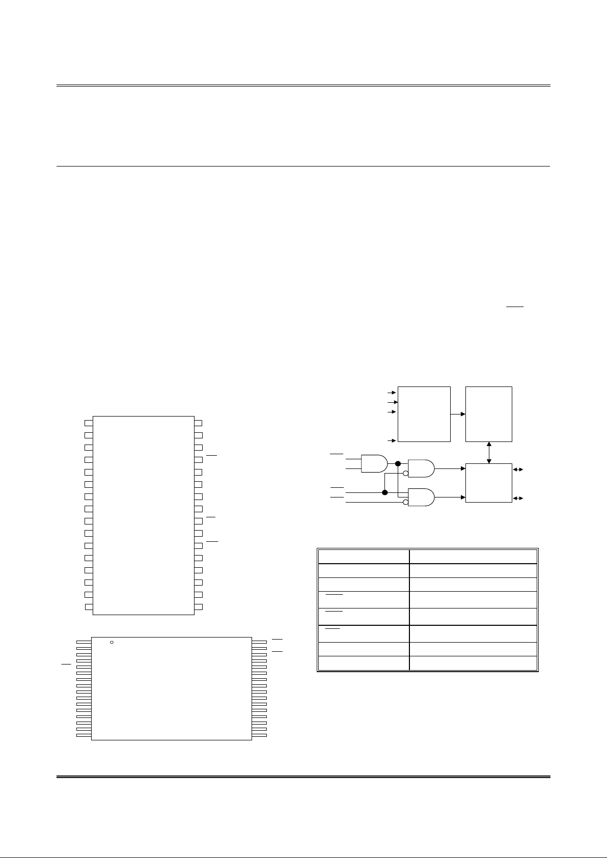
PIN CONFIGURATION
TSOP-I
1
2
3
4
5
6
7
8
9
10
11
12
13
14
15
16
32
31
30
29
28
27
26
25
24
23
22
21
20
19
18
17
A15
A14
A13
A12
WE
CE2
A11
VCC
NC
A10
A9
A8
A7
A6
A5
A4
OE
A16
CE1
I/O7
I/O6
I/O5
I/O4
I/O3
VSS
I/O2
I/O1
I/O0
A0
A1
A2
A3
GENERAL DESCRIPTION
The T14M1024A is a one-megabit density, fast
static random access memory organized as 131,072
words by 8 bits. It is designed for use in high
performance memory applications such as main
memory storage and high speed communication
buffers. Fabricated using high performance CMOS
technology, access times down to 10ns are achieved.
Memory expansion by banking is easily
accomplished using the chip enable pins
CE1 and
CE2. This device is packaged in a standard 32-pin
300 mil SOJ and 32-pin TSOP-I.
BLOCK DIAGRAM
PIN DESCRIPTION
SYMBOL DESCRIPTION
A0 - A16 Address Inputs
I/O0 - I/O7 Data Inputs/Outputs
CE1
,CE2
Chip Select Inputs
WE
Write Enable
OE
Output Enable
Vcc Power Supply
Vss Ground
PART NUMBER EXAMPLES
PACKAGE SPEED
T14M1024A-10J SOJ 300mil 10ns
T14M1024A-10P TSOP-I 8x13.4mm 10ns
T14M1024A-10H TSOP-I 8x20mm 10ns
A8
A9
A7
A6
A5
A3
A4
A2
A1
A0
I/O0
I/O1
A10
NC
28
27
26
25
23
24
22
21
20
19
18
17
32
29
1
2
3
4
6
5
7
8
9
10
11
12
15
16
Vcc
A12
A13
A14
A15
A16
I/O7
I/O6
I/O5
A11
CE2
WE
OE
CE1
I/O2
Vss
30
31
13
14
I/O4
I/O3
SOJ
DECODER
A0
A16
CE2
WE
OE
I/O7
Vcc
DATA I/O
CORE
ARRAY
Vss
CE1
I/O0
.
.
.
.
.
.
.
Page 2
TE
CH
tm
T14M1024A
TM Technology Inc. reserves the right P. 2 Publication Date: SEP. 2002
to change products or specifications without notice. Revision:E
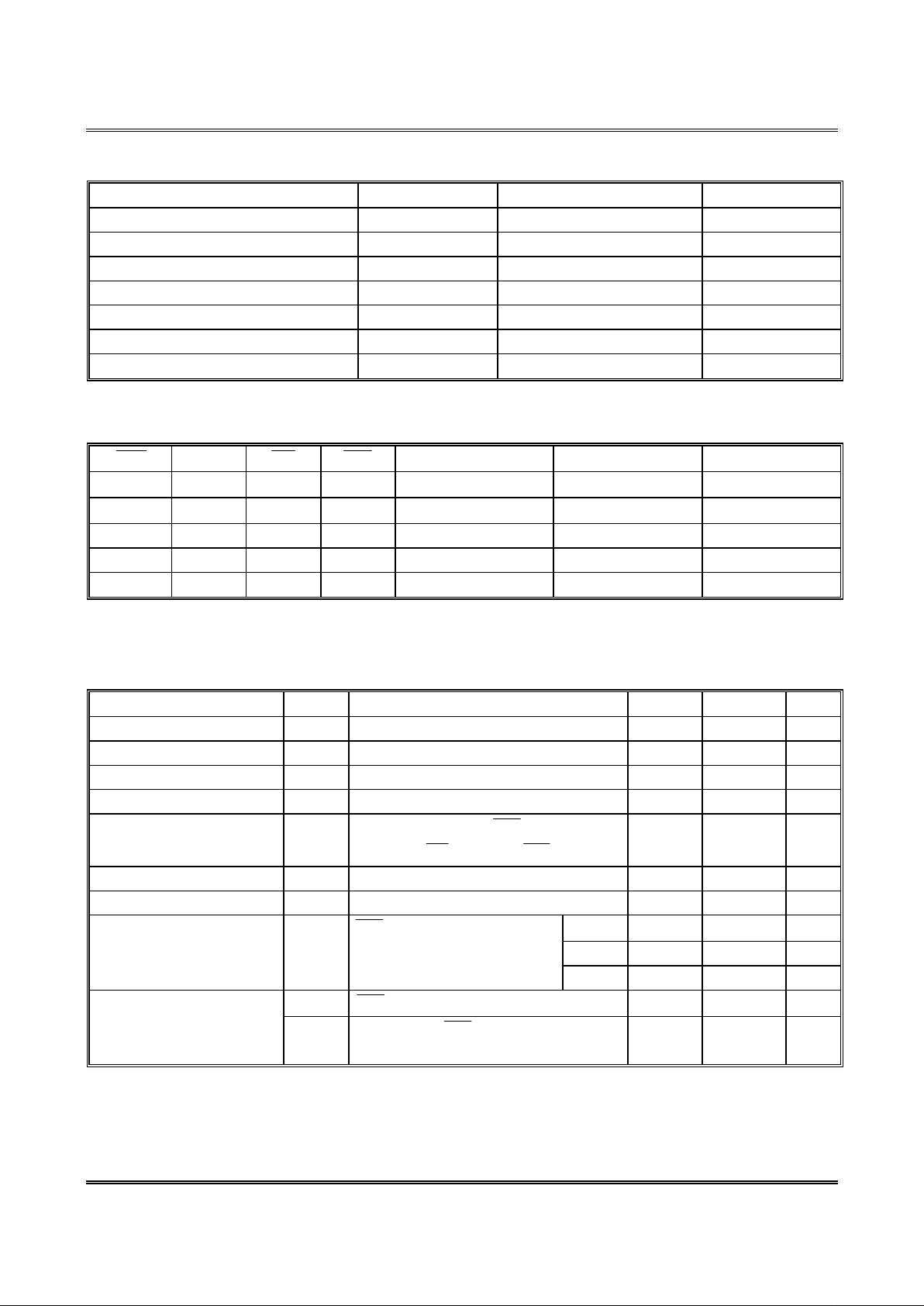
DC CHARACTERISTICS ABSOLUTE MAXIMUM RATINGS
PARAMETER SYM RATING UNIT
Power Supply Voltage Vcc -0.5 to 7.0 V
Input Voltage
V
IN
-0.5 to Vcc+0.5 V
Output Voltage
V
OUT
-0.5 to Vcc+0.5 V
Operating Temperatrue
T
OPR
0 to +70 °C
Storage Temperature
T
STG
-55 to +150 °C
Power Dissipation
P
D
1.0 W
Short Circuit Output Current
I
OUT
50 mA
TRUTH TABLE
CE1
CE2
OE
WE
MODE I/O0- I/O7 Vcc
H X X X Not Selected High-Z
I
SB,
I
SB1
X L X X Not Selected High-Z
I
SB,
I
SB1
L H H H Output Disable High-Z Icc
L H L H Read Data Out Icc
L H X L Write Data In Icc
OPERATING CHARACTERISTICS
(Vcc = 5V ± 10%, Ta = 0 to 70°C)
PARAMETER SYM. TEST CONDITIONS MIN. MAX. UNIT
Power Supply Voltage Vcc 4.5 5.5 V
Input Low Voltage
V
IL
-0.5 0.8 V
Input High Voltage
V
IH
2.2 Vcc+0.5 V
Input Leakage Current
I
LI
VIN =Vss to Vcc
- 5 uA
Output Leakage Current
I
LO
V
IN
=Vss to Vcc ,
CE1
= VIH or CE2
= V
IL
or
OE
= VIH or
WE
= VIL
- 5 uA
Output Low Voltage
V
OL
I
OL
= 4.0 mA
- 0.4 V
Output High Voltage
V
OH
IOH=-2.0 mA
2.4 - V
Operating Power Icc
CE1
=VIL
10ns - 110 mA
Supply Current
CE2 = V
IH
;f=max
12ns - 105 mA
IO = 0mA 15ns - 100 mA
Standby Power
I
SB
CE1
=VIH, CE2 = VIL, IO = 0mA
- 25 mA
Supply Current
I
SB1
Vcc = max;
CE1
≥ Vcc-0.2V or CE2
≤ Vss+0.2V; f=0mhz; IO = 0mA
- 5 mA
Note: Typical characteristics are at Vcc = 5V, Ta = 25°C
Page 3
TE
CH
tm
T14M1024A
TM Technology Inc. reserves the right P. 3 Publication Date: SEP. 2002
to change products or specifications without notice. Revision:E
RECOMMENDED OPERATING CONDITIONS
PARAMETER SYM MIN TYP MAX UNIT
Supply Voltage Vcc Typ-10% 5 Typ+10% V
Input Voltage, low
V
IL
-0.3 - 0.8 V
Input Voltage, high
V
IH
2.2 - Vcc+0.3 V
Ambient Temperature
T
A
0 - 70 °C
CAPACITANCE
PARAMETER SYMBOL CONDITION MAX. UNIT
Input Capacitance
C
IN
VIN = 0V
6 pF
Input/ Output Capacitance
C
I/O
V
OUT
= 0V
8 pF
Note: These parameters are sampled but not 100% tested.
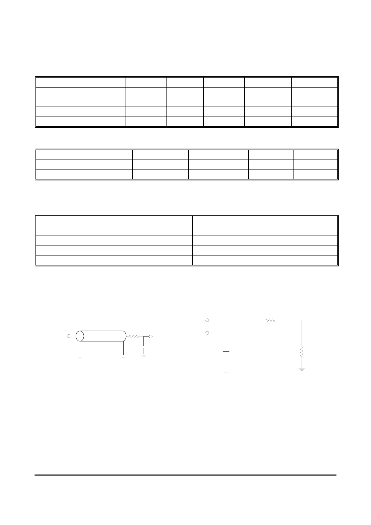
AC TEST CONDITIONS
PARAMETER CONDITIONS
Input Pulse Levels 0V to 3V
Input Rise and Fall Times 3.0 ns
Input and Output Timing Reference Level 1.5V
Output Load
C
L
=30pF,
I
OH
/
I
OL
= -2mA/4mA
AC TEST LOADS AND WAVEFORM
RL=50 ohm
OUTPUT
Zo=50 ohm 30pF
R1 480 ohm
5V
OUTPUT
5pF
Including
Jig and
Scope
R2
255 ohm
(For T
CLZ
, T
OLZ
, T
CHZ
, T
OHZ
, T
WHZ
, TOW )
Vt=1.5V
Page 4

TE
CH
tm
T14M1024A
TM Technology Inc. reserves the right P. 4 Publication Date: SEP. 2002
to change products or specifications without notice. Revision:E
AC CHARACTERISTICS
(
V
cc
=5V ± 10%, Vss = 0V, Ta = 0 to 70°C)
(1) READ CYCLE
T14M1024A-10 T14M1024A-12 T14M1024A-15
PARAMETER SYM.
MIN. MAX. MIN. MAX. MIN. MAX.
UNIT
Read Cycle Time
t
RC
10 - 12 - 15 -
ns
Address Access Time
t
AA
- 10 - 12 - 15 ns
Chip Enable Access Time
t
ACS
- 10 - 12 - 15 ns
Output Enable to Output Valid
t
AOE
- 6 - 7 - 7 ns
Chip Enable to Output in Low Z
t
CLZ*
3 - 3 - 3 - ns
Output Enable to Output in Low Z
t
OLZ*
0 - 0 - 0 - ns
Chip Disable to Output in High Z
t
CHZ*
- 5 - 6 - 7 ns
Output Disable to Output in High Z
t
OHZ*
- 5 - 6 - 7 ns
Output Hold from Address Change
t
OH
3 - 3 - 3 - ns
* These parameters are sampled but not 100% tested.
(2)WRITE CYCLE
T14M1024A-10 T14M1024A-12 T14M1024A-15
PARAMETER SYM.
MIN. MAX. MIN. MAX. MIN. MAX.
UNIT
Write Cycle Time
t
WC
10 - 12 - 15 -
ns
Chip Enable to End of Write
t
CW
8 - 10 - 11 - ns
Address Valid to End of Write
t
AW
8 - 10 - 11 - ns
Address Setup Time
t
AS
0 - 0 - 0 - ns
Write Pulse Width
t
WP
8 - 10 - 11 - ns
Write Recovery Time
t
WR
0 - 0 - 0 - ns
Data Valid to End of Write
t
DW
6 - 8 - 8 - ns
Data Hold from End of Write
t
DH
0 - 0 - 0 - ns
Write to Output in High Z
t
WHZ*
- 5 - 6 - 6 ns
Output Disable to Output in High Z
t
OHZ*
- 5 - 6 - 7 ns
Output Active from End of Write
t
OW
0 - 0 - 0 - ns
* These parameters are sampled but not 100% tested.
Page 5

TE
CH
tm
T14M1024A
TM Technology Inc. reserves the right P. 5 Publication Date: SEP. 2002
to change products or specifications without notice. Revision:E
TIMING WAVEFORMS
READ CYCLE 1
(Address Controlled)
t
RC
Address
t
OH
t
AA
D
OUT
t
OH
READ CYCLE 2
(Chip Enable Controlled)
DON'T CARE
UNDEFINED
t
RC
t
CLZ
t
CHZ
D
OUT
t
OHZ
t
OH
t
ACS
t
OLZ
t
AOE
t
AA
Address
CE
OE
Page 6

TE
CH
tm
T14M1024A
TM Technology Inc. reserves the right P. 6 Publication Date: SEP. 2002
to change products or specifications without notice. Revision:E
WRITE CYCLE 1 (OE CLOCK)
t
WC
t
OHZ
t
DW
D
IN
t
DH
t
WR
t
AS
t
WP
t
AW
t
CW
Addr ess
CE
OE
WE
(1,4)
D
OUT
WRITE CYCLE 2
(OE =
V
IL
Fixed)
DON'T CA RE
UNDEFINED
t
WC
t
OW
t
DW
D
IN
t
DH
t
WR
t
AS
t
WP
t
AW
t
CW
Add res s
CE
WE
(2)
D
OUT
t
OH
(3)
t
WHZ
(1,4)
Page 7

TE
CH
tm
T14M1024A
TM Technology Inc. reserves the right P. 7 Publication Date: SEP. 2002
to change products or specifications without notice. Revision:E
Notes: 1. During this period, I/O pins are in the output state, so input signals of opposite phase to the
outputs should not be applied.
2. The data output from
D
OUT
are the same as the data written to
D
IN
during the write cycle.
3.
D
OUT
provides the read data for the next address.
4. Transition is measured ± 500 mV from steady state with
C
L
= 5pF. This parameter is
guaranteed but not 100% tested.
5. If
OE is low during a WE controlled write cycle, the write pulse width must be the larger of
tWP or (t
WHZ
+ tDW) to allow the I/O drivers to turn off and data to be placed on the bus for the
required tDW. If
OE is high during a WE controlled write cycle, this requirement does
not apply and the write pulse can be as short as the specified tWP.
Page 8

TE
CH
tm
T14M1024A
TM Technology Inc. reserves the right P. 8 Publication Date: SEP. 2002
to change products or specifications without notice. Revision:E
PACKAGE DIMENSIONS
32-LEAD SOJ SRAM (300 mil)
SYMBOL DIMENSIONS IN INCHES DIMENSIONS IN MM
A 0.140(MAX) 3.556(MAX)
A1 0.026(MIN) 0.660(MIN)
A2 0.100±0.005 2.540±0.127
B 0.018(TYP) 0.457(TYP)
B1 0.028(TYP) 0.711(TYP)
C 0.008(TYP) 0.203(TYP)
D 0.823±0.005 20.904±0.127
E 0.335±0.010 8.509±0.254
E1 0.300±0.005 7.620±0.127
e 0.050(TYP) 1.270(TYP)
L 0.086±0.010 2.184±0.254
y 0.003(MAX) 0.076(MAX)
Page 9

TE
CH
tm
T14M1024A
TM Technology Inc. reserves the right P. 9 Publication Date: SEP. 2002
to change products or specifications without notice. Revision:E
PACKAGE DIMENSIONS
32-LEAD TSOP-I (8x20mm)
DIMENSIONS IN INCHES DIMENSIONS IN MM
SYMBOL
MIN NOM MAX MIN NOM MAX
A - - 0.047 - - 1.20
A1 0.002 - 0.006 0.05 - 0.15
A2 0.035 0.040 0.041 0.90 1.00 1.05
b 0.007 0.008 0.011 0.17 0.20 0.27
C 0.004 0.006 0.008 0.10 0.15 0.21
HD 0.787 TYP 20.00 TYP
D 0.724 TYP 18.40 TYP
E 0.315 TYP 8.00 TYP
e 0.020 TYP 0.50 TYP
L 0.020 0.024 0.028 0.50 0.60 0.70
L1 0.032 TYP 0.813 TYP
θ
0° 3° 5° 0° 3° 5°
HD
1
16 17
32
D
"A "
C
b
e
A2AA1
E
L
L1
Detai l "A "
Seat ing plane
Seat ing plane y
Page 10

TE
CH
tm
T14M1024A
TM Technology Inc. reserves the right P. 10 Publication Date: SEP. 2002
to change products or specifications without notice. Revision:E
PACKAGE DIMENSIONS
32-LEAD TSOP-I (8x13.4mm)
DIMENSIONS IN INCHES DIMENSIONS IN MM
SYMBOL
MIN NOM MAX MIN NOM MAX
A - - 0.047 - - 1.20
A1 0.002 - 0.006 0.05 - 0.15
A2 0.035 0.040 0.041 0.90 1.00 1.05
b 0.007 0.008 0.011 0.17 0.20 0.27
C 0.004 0.006 0.008 0.10 0.15 0.21
HD 0.528 TYP 13.40 TYP
D 0.465 TYP 11.80 TYP
E 0.315 TYP 8.00 TYP
e 0.020 TYP 0.50 TYP
L 0.020 0.024 0.028 0.50 0.60 0.7
L1 0.032TYP 0.813 TYP
θ
0° 3° 5° 0° 3° 5°
HD
1
16 17
32
D
"A "
C
b
e
A2AA1
E
L
L1
D e ta il "A"
Seating plane
Seating plane y
 Loading...