

Page 1
TE
C
H
tm
VSS→
Vcc
→
CS
WE
OE
T14L256A
SRAM
FEATURES
•
High speed access time: 8/10/12/15ns(max.)
• Low power consumption : Active 300 mW (typ.)
•
Single + 3.3 power supply
•
Fully static operation – No clock or refreshing
required
•
All inputs and outputs directly LVTTL compatible
•
Comm on I/O capability
•
Available packages :28-pin 300 mil, SOJ and
TSOP-I (forward type).
•
Output enable (OE) available for very fast
access
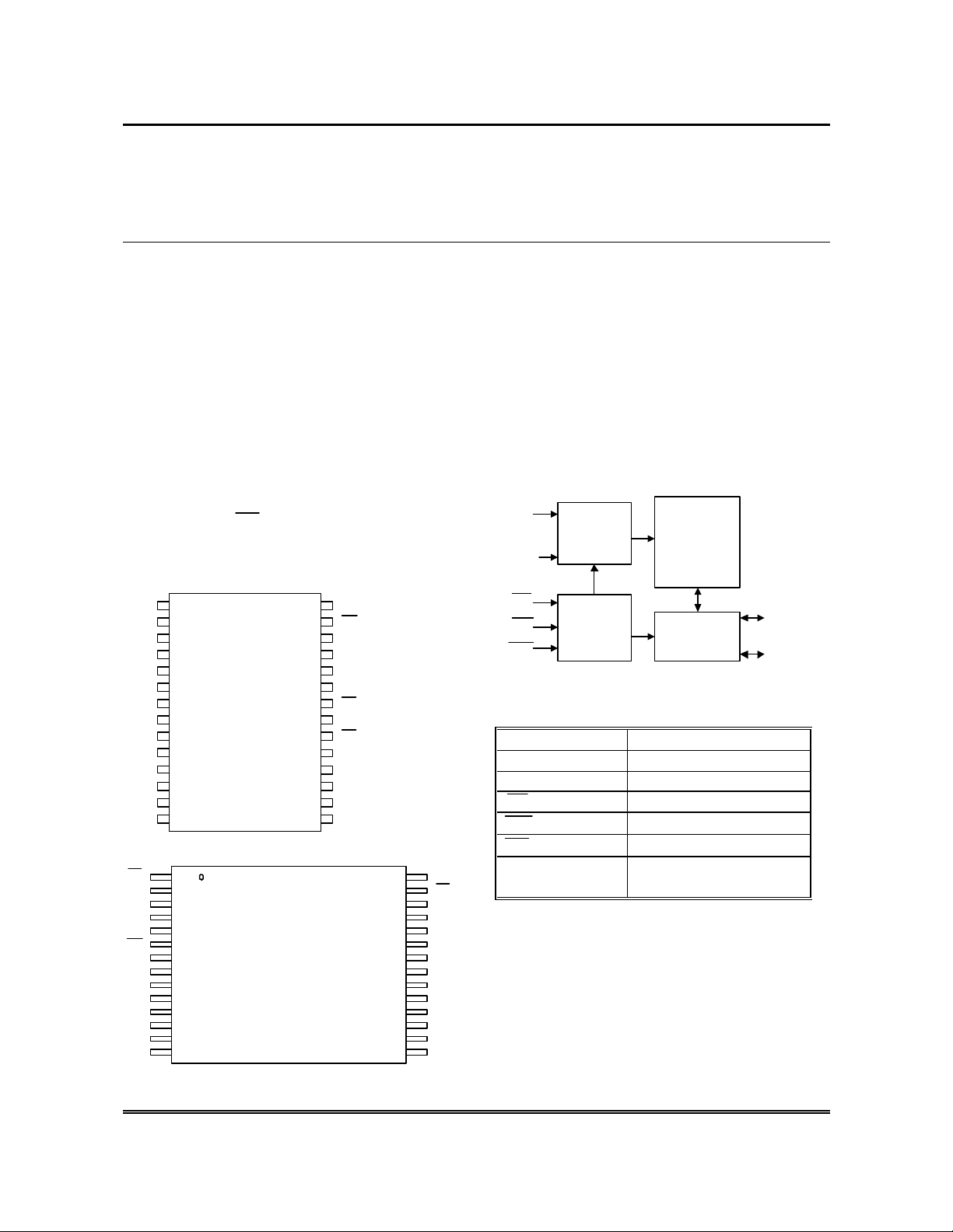
PIN CONFIGURATION
A14
A12
A7
A6
A5
A4
A3
A2
A1
A0
I/O1
I/O2
I/O3
Vss
OE
A11
A9
A8
A13
WE
VCC
A14
A12
A7
A6
A5
A4
A3
1
2
3
4
5
6
7
SOJ
8
9
10
11
12
13
14
1
2
3
4
5
6
7
8
9
10
11
12
13
14
28
27
26
25
24
23
22
21
20
19
18
17
16
15
TSOP-I
Vcc
WE
A13
A8
A9
A11
OE
A10
CS
I/O8
I/O7
I/O6
I/O5
I/O4
28
27
26
25
24
23
22
21
20
19
18
17
16
15
A10
CS
I/O8
I/O7
I/O6
I/O5
I/O4
VSS
I/O3
I/O2
I/O1
A0
A1
A2
32K X 8 HIGH SPEED
CMOS STATIC RAM
GENERAL DESCRIPTION
The T14L256A is a high speed, low power
CMOS static RAM organized as 32,768 x 8 bits
that operates on a single 3.3-volt power supply.
This device is packaged in a standard 28-pin 300
mil SOJ or TSOP-I forward.
BLOCK DIAGRAM
A 0
.
DECODER
.
.
A 14
CS
OE
WE
CONTROL
PIN DESCRIPTION
SYMBOL DESCRIPTION
A0 - A14 Address Inputs
I/O1 - I/O8 Data Inputs/Outputs
Vcc Power Supply
Vss Ground
PART NUMBER EXAMPLES
PACKAGE SPEED
T14L256A-8J SOJ 8ns
T14L256A-8P TSOP-I
CORE
ARRAY
DATA I/O
Chip Select Inputs
Write Enable
Output Enable
8ns
I/O 1
.
.
.
I/O 8
Taiwan Memory Technology, Inc. reserves the right P. 1 Publication Date: APR. 2001
to change products or specifications without notice. Revision: E
Page 2
TE
C
H
tm
V
IL
IH
A
I
I
SB1
I
LI
LO
CS
IH
OE
V
IH
WE
V
IL
OL
OL
OH
OH
2.4
CS
V
IL
SB
CS
IH
SB1
CS
cc
T14L256A
DC CHARACTERISTICS ABSOLUTE MAXIMUM RATINGS
PARAMETER RATING UNIT
Supply Voltage to Vss Potential -0.5 to + 4.6 V
Inputs to Vss Potential -0.5 to Vcc +0.5 V
Power Dissipation 1.0 W
Storage Temperature -60 to +150
RECOMMENDED OPERATING CONDITIONS
PARAMETER SYM MIN TYP MAX UNIT
Supply Voltage Vcc Typ-5% 3.3 Typ+ 5% V
V
T
-0.3 - 0.8 V
2.1 - Vcc+0.3 V
0 - 70 °C
Input Voltage, low
Input Voltage, high
Ambient Temperature
TRUTH TABLE
°
C
CS
OE
WE
MODE I/O1- I/O8 Vcc
H X X Not Selected High -Z
L H H Output Disable High-Z Icc
L L H Read Data Out Icc
L X L Write Data In Icc
OPERATING CHARACTERISTICS
(Vcc = 3.3V ± 5%, Vss = 0V, Ta = 0 to 70°C)
PARAMETER SYM. TEST CONDITIONS MIN. TYP. MAX. UNIT
Input Leakage Current
Output Leakage Current
Output Low Voltage
Output High Voltage
Operating Power
Supply Current
Standby Power
Supply Current I
Vin=Vss to Vcc -10 - +10 uA
V
V
I
Icc
V
I/O
=
I
= + 8.0mA
I
= - 4.0mA
Cycle = MIN.
Duty = 100%
=Vss to Vcc ,
or
=
, I/O=0mA
=
=
V
or
-10 - +10 uA
- - 0.4 V
- - V
8 - - 110 mA
10 - - 100 mA
12 - - 90 mA
15 - - 80 mA
I
V
=
, Cycle=MIN, Duty=100%
V
≥
-0.2V
- - 15 mA
- - 2 mA
SB,
Note: Typical characteristics are at Vcc = 3.3V, Ta = 25°C
Taiwan Memory Technology, Inc. reserves the right P. 2 Publication Date: APR. 2001
to change products or specifications without notice. Revision: E
Page 3
TE
C
H
tm
IN
IN
I/O
OUT
C
L
I
OH
I
OL
T14L256A
CAPACITANCE
(Vcc = 3.3V, Ta = 25°C, f = 1 MHz)
PARAMETER SYMBOL CONDITION MAX. UNIT
C
Input Capacitance
Input/ Output Capacitance
Note: These parameters are sampled but not 100% tested.
C
AC TEST CONDITIONS
PARAMETER CONDITIONS
Input Pulse Levels 0V to 3V
Input Rise and Fall Times 3 ns
Input and Output Timing Reference Level 1.5V
Output Load
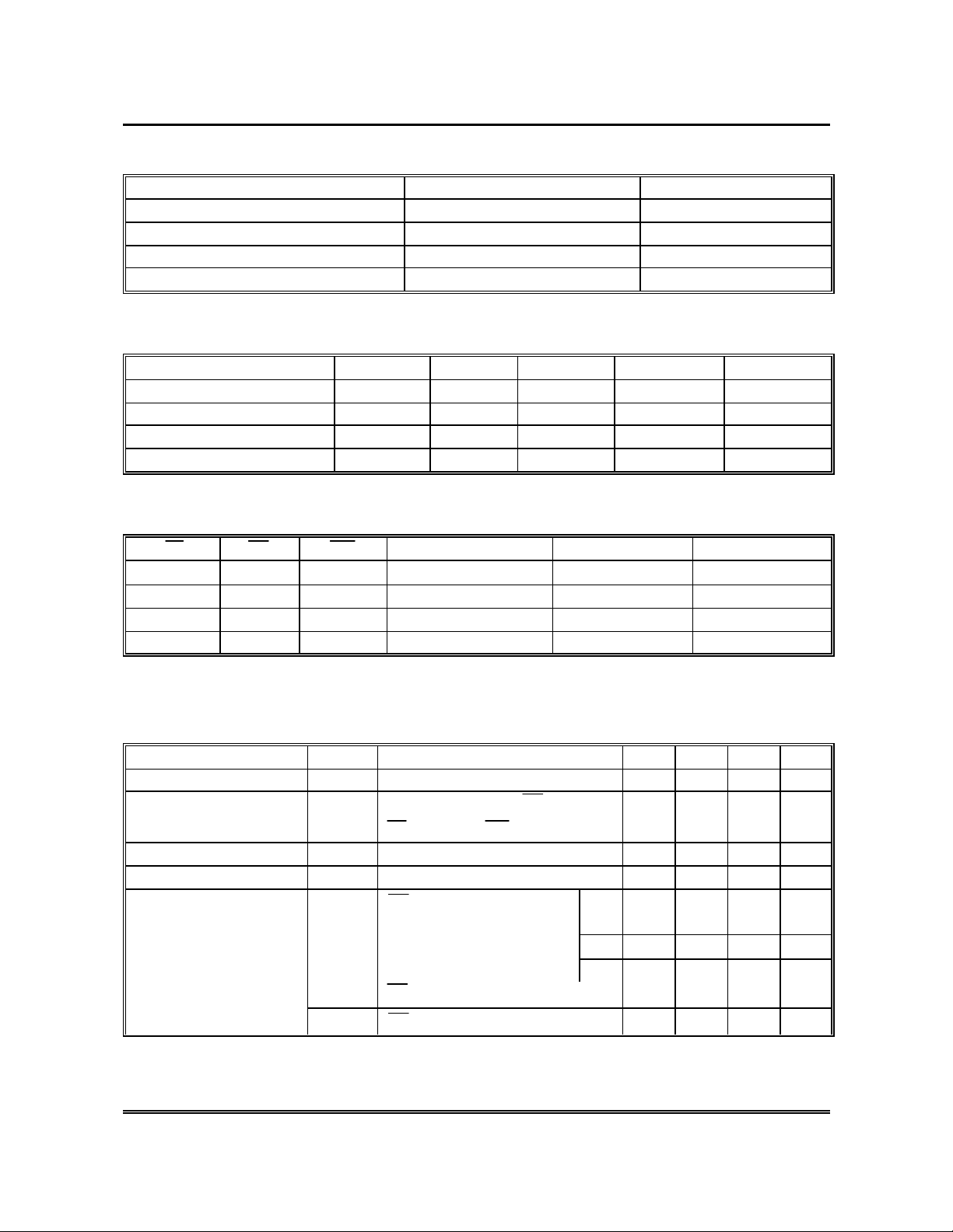
AC TEST LOADS AND WAVEFORM
3.3V
OUTPUT
R1 320 ohm
30pF
Including
Jig and
Scope
OUTPUT
R2
350 ohm
V
V
=30pF,
3.3V
= 0V
= 0V
/
= -4mA/8mA
R1 320 ohm
5pF
Including
Jig and
Scope
6 pF
8 pF
R2
350 ohm
(For TCLZ, TOLZ, TCHZ, TOHZ, TWHZ, TOW )
3.0V
0 V
3ns
Taiwan Memory Technology, Inc. reserves the right P. 3 Publication Date: APR. 2001
to change products or specifications without notice. Revision: E
90%
10% 10%
90%
3ns
Page 4

TE
C
H
tm
cc
T14L256A
AC CHARACTERISTICS
(
=3.3V ± 5%, Vss = 0V, Ta = 0 to 70°C)
V
(1) READ CYCLE
T14L256A-8 T14L256A-10 T14L256A-12 T14L256A-1
MIN. MAX. MIN. MAX. MIN. MAX. MIN. MAX.
Read Cycle Time
Address Access Time
Chip Select Access Time
Output Enable to Output Valid
Chip Selection to Output in Low Z
Output Enable to Output in Low Z
Chip Deselection to Output in High Z
Output Disable to Output in High Z
Output Hold from Address Change
* These parameters are sampled but not 100% tested.
RC
t
AA
t
ACS - 8 - 10 - 12 - 15 ns
t
AOE
t
CLZ* 3 - 3 - 3 - 3 - ns
t
OLZ
t
CHZ* - 4 - 5 - 6 0 7 ns
t
OHZ - 4 - 5 - 6 0 7 ns
t
OH 2.5 - 3 - 3 - 3 - ns
t
8 - 10 - 12 - 15 - ns
- 8 - 10 - 12 - 15 ns
- 5 - 6 - 7 - 7 ns
0 - 0 - 0 - 0 - ns
(2)WRITE CYCLE
PARAMETER SYM.
Write Cycle Time
Chip Selection to End of Write
Address Valid to End of Write
T14L256A-8 T14L256A-10 T14L256A-12 T14L256A-15
MIN. MAX. MIN. MAX. MIN. MAX. MIN. MAX.
WC 8 - 10 - 12 - 15 - ns
t
CW 6 - 8 - 10 - 11 - ns
t
AW 6 - 8 - 10 - 11 - ns
t
UNIT
5 PARAMETER SYM.
UNIT
Address Setup Time
Write Pulse Width
Write Recovery Time
Data Valid to End of Write
Data Hold from End of Write
Write to Output in High Z
Output Disable to Output in High Z
Output Active from End of Write
* These parameters are sampled but not 100% tested.
Taiwan Memory Technology, Inc. reserves the right P. 4 Publication Date: APR. 2001
to change products or specifications without notice. Revision: E
AS
t
WP 6 - 8 - 10 - 11 - ns
t
WR
t
DW 5 - 6 - 8 - 8 - ns
t
DH
t
WHZ - 4 - 5 - 6 - 6 ns
t
OHZ - 4 - 5 - 6 - 7 ns
t
OW 0 - 0 - 0 - 0 - ns
t
0 - 0 - 0 - 0 - ns
0 - 0 - 0 - 0 - ns
0 - 0 - 0 - 0 - ns
Page 5

TE
C
H
tm
T14L256A
TIMING WAVEFORMS
READ CYCLE 1
(Address Controlled)
A d d r e s s
t
OH
D
O U T
READ CYCLE 2
(Chip Select Controlled)
C S
t
CL Z
t
R C
t
AA
t
OH
t
A CS
t
CH Z
D
O U T
READ CYCLE 3
(Output Enable Controlled)
A d d r e s s
O E
C S
D
O U T
t
t
t
t
t
AOE
OLZ
AC S
CL Z
AA
t
RC
t
OH
t
OH Z
t
CH Z
DON 'T CA R E
UN DE F IN E D
Taiwan Memory Technology, Inc. reserves the right P. 5 Publication Date: APR. 2001
to change products or specifications without notice. Revision: E
Page 6

TE
C
H
tm
V
IL
T14L256A
WRITE CYCLE 1 (OE CLOCK)
A d d r e s s
O E
CS
t
t
WC
CW
t
t
AW
WP
t
WR
WE
D
OU T
D
I N
WRITE CYCLE 2
A d d r e s s
C S
W E
D
O U T
(OE =
t
t
AS
t
OHZ
AS
(1 ,4)
Fixed)
t
WH Z
t
DW
t
DH
t
WC
t
CW
t
AW
t
WP
(1 ,4 )
t
D W
t
WR
t
OH
t
OW
(2 )
t
DH
(3)
D
I N
D O N 'T CA R E
U N DE F I NE D
Taiwan Memory Technology, Inc. reserves the right P. 6 Publication Date: APR. 2001
to change products or specifications without notice. Revision: E
Page 7

TE
C
H
tm
OUT
IN
OUT
L
OE
WE
T14L256A
Notes: 1. During this period, I/O pins are in the output state, so input signals of opposite phase to the outputs
should not be applied.
2. The data output from
3.
4. Transition is measured ± 500 mV from steady state with
5. If
D
provides the read data for the next address.
guaranteed but not 100% tested.
OE
is low during a
tWP or (t
required tDW. If
apply and the write pulse can be as short as the specified tWP.
WHZ
D
are the same as the data written to
WE
controlled write cycle, the write pulse width must be the larger of
+ tDW) to allow the I/O drivers to turn off and data to be placed on the bus for the
is high during a
controlled write cycle, this requirement does not
C
D
during the write cycle.
= 5pF. This parameter is
Taiwan Memory Technology, Inc. reserves the right P. 7 Publication Date: APR. 2001
to change products or specifications without notice. Revision: E
Page 8

TE
C
H
tm
T14L256A
PACKAGE DIMENSIONS
28-LEAD SOJ SRAM (300 mil)
SYMBOL DIMENSIONS IN INCHES DIMENSIONS IN MM
A 0.710±0.002 18.03±0.05
B 0.300±0.005 7.62±0.13
C 0.060±0.002 1.52±0.05
D 0.050±0.001 1.27±0.03
E 0.063±0.001 1.63±0.03
F 0.015±0.002 0.38±0.05
G 0.030±0.002 0.76±0.05
H 0.050±0.002 1.27±0.05
I 0.018±0.002 0.46±0.05
J 0.028±0.002 0.71±0.05
K 0.337±0.002 8.56±0.05
L 0.010±0.001 0.25±0.03
M 0.026±0.002 0.66±0.05
N 0.268±0.003 6.81±0.08
O 0.300±0.002 7.62±0.05
P 0.053±0.001 1.35±0.03
Q 0.140±0.004 3.56±0.10
y 0.004(MAX) 0.10(MAX)
Taiwan Memory Technology, Inc. reserves the right P. 8 Publication Date: APR. 2001
to change products or specifications without notice. Revision: E
Page 9

TE
C
H
tm
T14L256A
PACKAGE DIMENSIONS
28-LEAD TSOP-I SRAM (8X13.4mm)
D
C
1
14 15
Db
Seating plane
28
"A"
Gauge plane
Detail "A"
b
E
e
A2AA1
Seating plane y
0.010
L
L1
SYMBOL DIMENSIONS IN INCHES DIMENSIONS IN MM
A 0.047(max.) 1.20(max.)
A1 0.004±0.002 0.10±0.05
A2 0.039±0.002 1.00±0.05
b 0.008(typ.) 0.20(typ.)
c 0.006(typ.) 0.15(typ.)
Db 0.465±0.004 11.80±0.10
E 0.315±0.004 8.00±0.10
e 0.022(typ.) 0.55(typ.)
D 0.528±0.008 13.40±0.20
L 0.020±0.004 0.50±0.10
L1 0.0315±0.004 0.80±0.10
y 0.004(max.) 0.10(max.)
0°~5° 0°~5°
θ
Taiwan Memory Technology, Inc. reserves the right P. 9 Publication Date: APR. 2001
to change products or specifications without notice. Revision: E
 Loading...