

Page 1
PROGRAMMABLE
T
A
D
FREQUENCY SYNTHESIZER
(25MHz to 400MHz)
ClockWorks™
SY89429A
FEATURES
■ Improved jitter performance over SY89429
■ 25MHz to 400MHz differential PECL outputs
■ ±25ps peak-to-peak output jitter
■ Minimal frequency over-shoot
■ Synthesized architecture
■ Serial 3 wire interface
■ Parallel interface for power-on
■ Internal quartz reference oscillator driven by quartz
crystal or PECL source
■ PECL output can operate with either +3.3V or +5V
VCC_OUT power supply
■ External loop filter optimizes performance/cost
■ Applications note (AN-06) for ease of design-ins
■ Available in PLCC and SOIC 28-pin packages
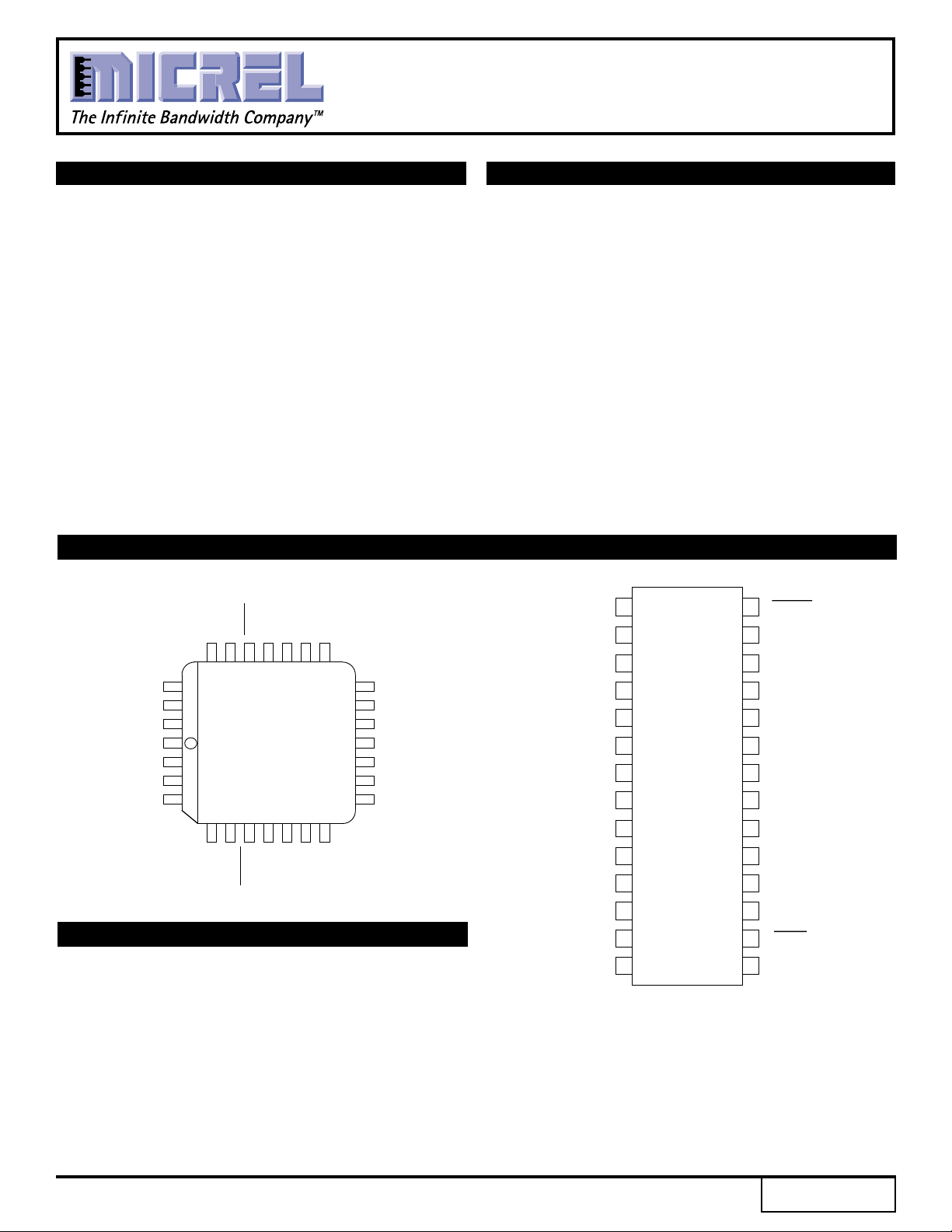
PIN CONFIGURATION
S
_CLOCK
S_DAT
S_LOA
VCC_QUIE
LOOP _FILTER
LOOP_REF
XTAL1
CC_OUT
V
FOUT
25 24 23 22 21 20 19
26
27
28
1
2
3
4
TOP VIEW
567891011
VCC1
XTAL2
FOUT
PLCC
_LOAD
P
GND
M[0]
CC (TTL)
V
M[1]
TEST
GND (TTL)
M[3]
M[2]
18
N[1]
17
N[0]
16
M[8]
15
M[7]
14
M[6]
13
M[5]
12
M[4]
APPLICATIONS
■ Workstations
■ Advanced communications
■ High end consumer
■ High-performance computing
■ RISC CPU clock
■ Graphics pixel clock
■ Test equipment
■ Other high-performance processor-based
applications
DESCRIPTION
The SY89429A is a general purpose, synthesized clock
source targeting applications that require both serial and
parallel interfaces. Its internal VCO will operate over a
range of frequencies from 400MHz to 800MHz. The
differential PECL output can be configured to be the VCO
frequency divided by 2, 4, 8 or 16. With the output configured
to divide the VCO frequency by 2, and with a 16MHz
external quartz crystal used to provide the reference
frequency, the output frequency can be specified in 1MHz
steps.
M[0]
M[1]
M[2]
M[3]
M[4]
M[5]
M[6]
M[7]
M[8]
N[0]
N[1]
GND (TTL)
TEST
CC
(TTL)
V
1
2
3
4
5
6
7
8
9
10
11
12
13
14
TOP VIEW
SOIC
Z28-1
28
P
_LOAD
27
V
CC1
26
XTAL
2
25
XTAL
1
24
LOOP
_REF
23
LOOP
_FILTER
22
V
CC_QUIET
21
S
_LOAD
20
S
_DATA
19
S
_CLOCK
18
V
CC_OUT
17
FOUT
16
FOUT
15
GND
Rev.: H Amendment: /0
1
Issue Date: October, 1998
Page 2

Micrel
BLOCK DIAGRAM
ClockWorks™
SY89429A
+5.0V
÷ 8
10-25MHz
Fundamental
Crystal
or
OSC
PECL
Source
3 WIRE
INTERFACE
DETAILED BLOCK DIAGRAM
LOOP_FILTER
F
REF
PHASE DETECTOR
PLL
VCO
PECL
÷ M
400 – 800
÷ N
MHz
SERIAL
PARALLEL
INTERFACE
LOGIC
CONFIG INFO
+5.0V
23 1
LOOP_REF
V
CC_QUIET
+5.0V
V
CC1
FOUT
TEST
6, 21
÷ 8
10–25MHz
Fundamental
Crystal
or
PECL
Source
S_
S_
P_
S_
LOAD
LOAD
DATA
CLOCK
4
XTAL1
5
28
7
27
26
OSC
XTAL2
NOTE:
Pin numbers reference PLCC pinout.
FREF
PHASE DETECTOR
COUNTER
L = LATCH
H = Transparent
9-BIT SR
8 -> 16
400-800
VCO
10
9-BIT ÷ M
LATCH LATCH
01
9
M[8:0]
MHz
T110
(2,4,8,16)
01
2-BIT SR
17,18
÷ N
N[1:0]
+5.0V
V
CC_OUT
÷ M —
LOW —
FOUT —
÷ M —
FREF —
HIGH —
7
6
5
4
3
2
1
0
FOUT ÷ 4 —
CLOCK
S_
LATCH
3-BIT SR
19,22
2
25
24
FOUT
23
FOUT
20
TEST
2
Page 3
Micrel
PIN DESCRIPTIONS
ClockWorks™
SY89429A
INPUTS
XTAL1, XTAL2
These pins form an oscillator when connected to an external
crystal. The crystal is series resonant. Alternatively, these
pins can be driven with 100K PECL level by an external
source.
S_LOAD
This TTL pin loads the configuration latches with the contents
of the shift registers. The latches will be transparent when this
signal is HIGH; thus, the register data must be stable on the
HIGH-to-LOW transition of S_LOAD for proper operation.
S_DATA
This TTL pin is the input to the serial configuration shift
registers.
S_CLOCK
This TTL pin clocks the serial configuration shift registers. On
the rising edge of this signal, data from S_DATA is sampled.
P_LOAD
This TTL pin loads the configuration latches with the contents
of the parallel inputs. The latches will be transparent when this
signal is LOW; thus, the parallel data must be stable on the
LOW-to-HIGH transition of P_LOAD for proper operation.
OUTPUTS
FOUT, FOUT
These differential positive-referenced ECL signals (PECL)
are the output of the synthesizer.
TEST
The function of this TTL output is determined by the serial
configuration bits T[2:0].
POWER
VCC1
This is the positive supply for the chip and is normally connected
to +5.0V.
VCC_OUT
This is the positive reference for the PECL outputs, FOUT and
FOUT. It is constrained to be less than or equal to VCC1.
VCC_QUIET
This is the positive supply for the PLL and should be as noisefree as possible for low-jitter operation.
GND
These pins are the negative supply for the chip and are
normally all connected to ground.
M[8:0]
These TTL pins are used to configure the PLL loop divider.
They are sampled on the LOW-to-HIGH transition of P_LOAD.
M[8] is the MSB, M[0] is the LSB. The binary count on the M
pins equates to the divide-by value for the PLL.
N[1:0]
These TTL pins are used to configure the output divider
modulus. They are sampled on the LOW-to-HIGH transition
of P_LOAD.
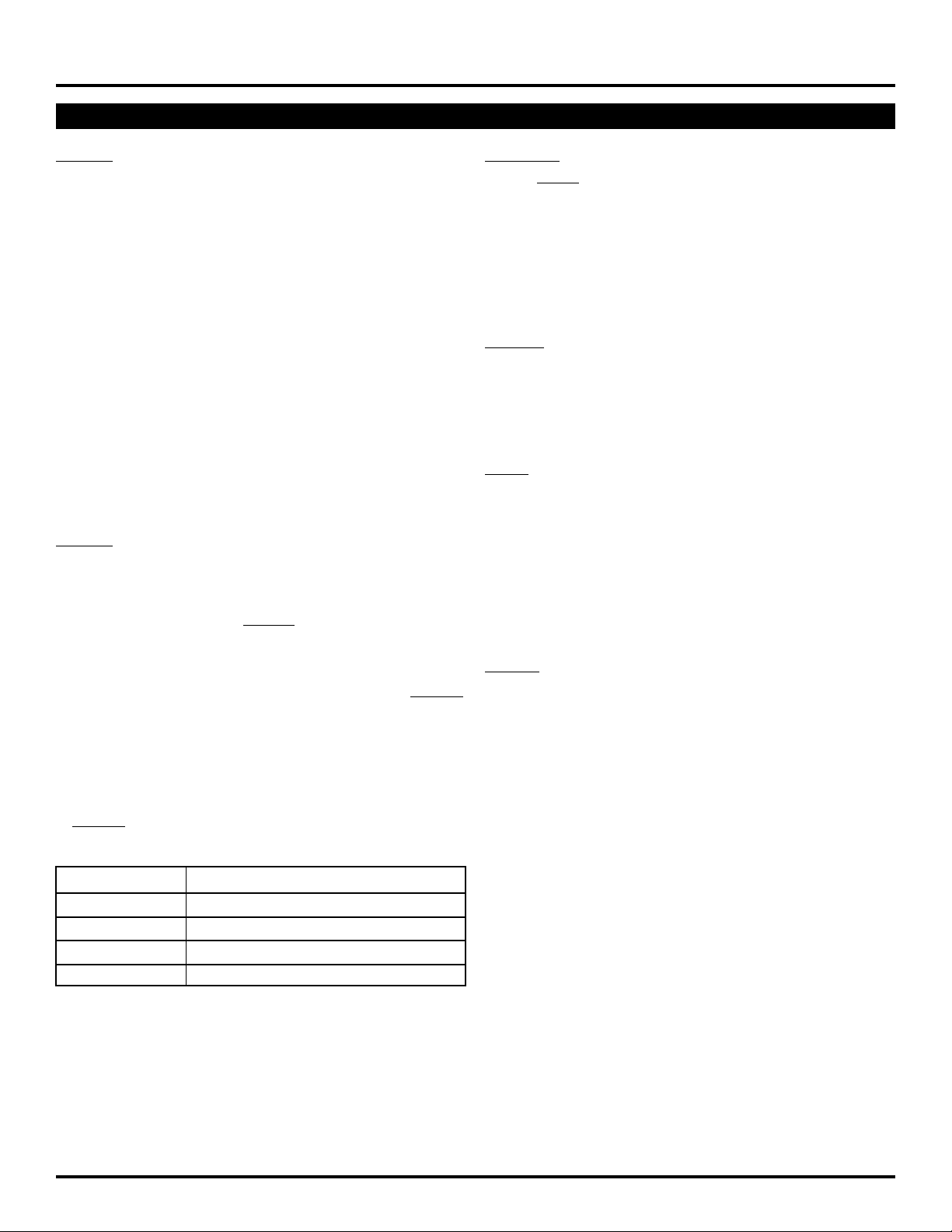
N[1:0] Output Division
0 0 2
0 1 4
1 0 8
1 1 16
OTHER
LOOP_FILTER
This is an analog I/O pin that provides the loop filter for the
PLL.
LOOP_REF
This is an analog I/O pin that provides a reference voltage for
the PLL.
3
Page 4
ClockWorks™
Micrel
SY89429A
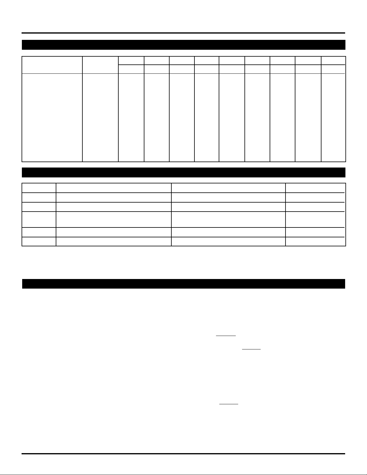
WITH 16MHZ INPUT
VCO Frequency 256 128 64 32 16 8421
(MHz) M Count M8 M7 M6 M5 M4 M3 M2 M1 M0
400 200 011001000
402 201 011001001
404 202 011001010
406 203 011001011
• • •••••••••
• • •••••••••
• • •••••••••
794 397 110001101
796 398 110001110
798 399 110001111
800 400 110010000
ABSOLUTE MAXIMUM RATINGS
Symbol Parameter Value Unit
VCC Power Supply Voltage –0.5 to +7.0 V
VI Input Voltage –0.5 to +7.0 V
I
OUT Output Source Continuous 50 mA
Tstore Storage Temperature –65 to +150 °C
A Operating Temperature –0 to +75 °C
T
NOTE:
1. Permanent device damage may occur if ABSOLUTE MAXIMUM RATINGS are exceeded. This is a stress rating only and functional operation is not implied at
conditions other than those detailed in the operational sections of this data sheet. Exposure to ABSOLUTE MAXIMUM RATlNG conditions for extended periods may
affect device reliability.
(1)
Surge 100
FUNCTIONAL DESCRIPTION
The internal oscillator uses the external quartz crystal as the
basis of its frequency reference. The output of the reference
oscillator is divided by eight before being sent to the phase
detector. With a 16MHz crystal, this provides a reference frequency
of 2MHz.
The VCO within the PLL operates over a range of 400–
800MHz. Its output is scaled by a divider that is configured by
either the serial or parallel interfaces. The output of this loop
divider is also applied to the phase detector.
The phase detector and loop filter force the VCO output
frequency to be M times the reference frequency by adjusting the
VCO control voltage. Note that for some values of M (either too
high or too low) the PLL will not achieve loop lock. External loop
filter components are utilized to allow for optimal phase jitter
performance.
The output of the VCO is also passed through an output
divider before being sent to the PECL output driver. The output
divider is configured through either the serial or the parallel
interfaces and can provide one of four divider ratios (2, 4, 8 or 16).
This divider extends the performance of the part while providing
a 50% duty cycle.
The output driver is driven differentially from the output divider
and is capable of driving a pair of transmission lines terminated
in 50Ω. The positive reference for the output driver is provided by
a dedicated power pin (VCC_OUT) to reduce noise and provide
application flexibility.
The configuration logic has two sections: serial and parallel.
The parallel interface uses the values at the M[8:0] and N[1:0]
inputs to configure the internal counters. Normally upon system
reset, the P_LOAD input is held LOW until sometime after
power becomes valid. With S_LOAD held LOW, on the LOWto-HIGH transition of P_LOAD, the parallel inputs are captured.
The parallel interface has priority over the serial interface.
Internal pull-up resistors are provided on the M[8:0] and N[1:0]
inputs to reduce component count.
The serial interface logic is implemented with a 14-bit shift
register scheme. The register shifts once per rising edge of the
S_CLOCK input. The serial input S_DATA must meet set-up and
hold timing as specified in the AC parameters section of this data
sheet. With P_LOAD held HIGH, the configuration latches will
capture the value in the shift register on the HIGH-to-LOW edge
of the S_LOAD input. See the programming section for more
information.
The TEST output reflects various internal node values and is
controlled by the T[2:0] bits in the serial data stream. See the
programming section for more information.
4
Page 5
Micrel
PROGRAMMING INTERFACE
ClockWorks™
SY89429A
Programming the device is accomplished by properly
configuring the internal dividers to produce the desired
frequency at the outputs. The output frequency can be
represented by this formula:
M
N
Where F
FOUT = ( ) x
XTAL is the crystal frequency, M is the loop divider
FXTAL
8
modulus, and N is the output divider modulus. Note that it is
possible to select values of M such that the PLL is unable to
achieve loop lock. To avoid this, always make sure that M is
selected to be 200 ≤ M ≤ 400 for a 16MHz input reference.
M[8:0] and N[1:0] are normally specified once at power-on,
through the parallel interface, and then possibly again through
the serial interface. This approach allows the designer to bring
up the application at one frequency and then change or finetune the clock, as the ability to control the serial interface
becomes available. To minimize transients in the frequency
domain, the output should be varied in the smallest step size
possible.
T2 T1 T0 TEST FOUT / FOUT
0 0 0 Data Out – Last Bit SR FVCO ÷ N
0 0 1 HIGH FVCO ÷ N
0 1 0 FREF FVCO ÷ N
0 1 1 M Counter Output FVCO ÷ N
1 0 0 FOUT FVCO ÷ N
1 0 1 LOW FVCO ÷ N
110S_CLOCK ÷ MS_CLOCK ÷ N
1 1 1 FOUT ÷ 4 FVCO ÷ N
The TEST output provides visibility for one of several
internal nodes (as determined by the T[1:0] bits in the serial
configuration stream). It is not configurable through the parallel
interface. Although it is possible to select the node that
represents FOUT, the TTL output may not be able to toggle
fast enough for some of the higher output frequencies. The T2,
T1, T0 configuration latches are preset to 000 when P_LOAD
is low, so that the FOUT outputs are as jitter-free as possible.
The serial configuration port can be used to select one of the
alternate functions for this pin.
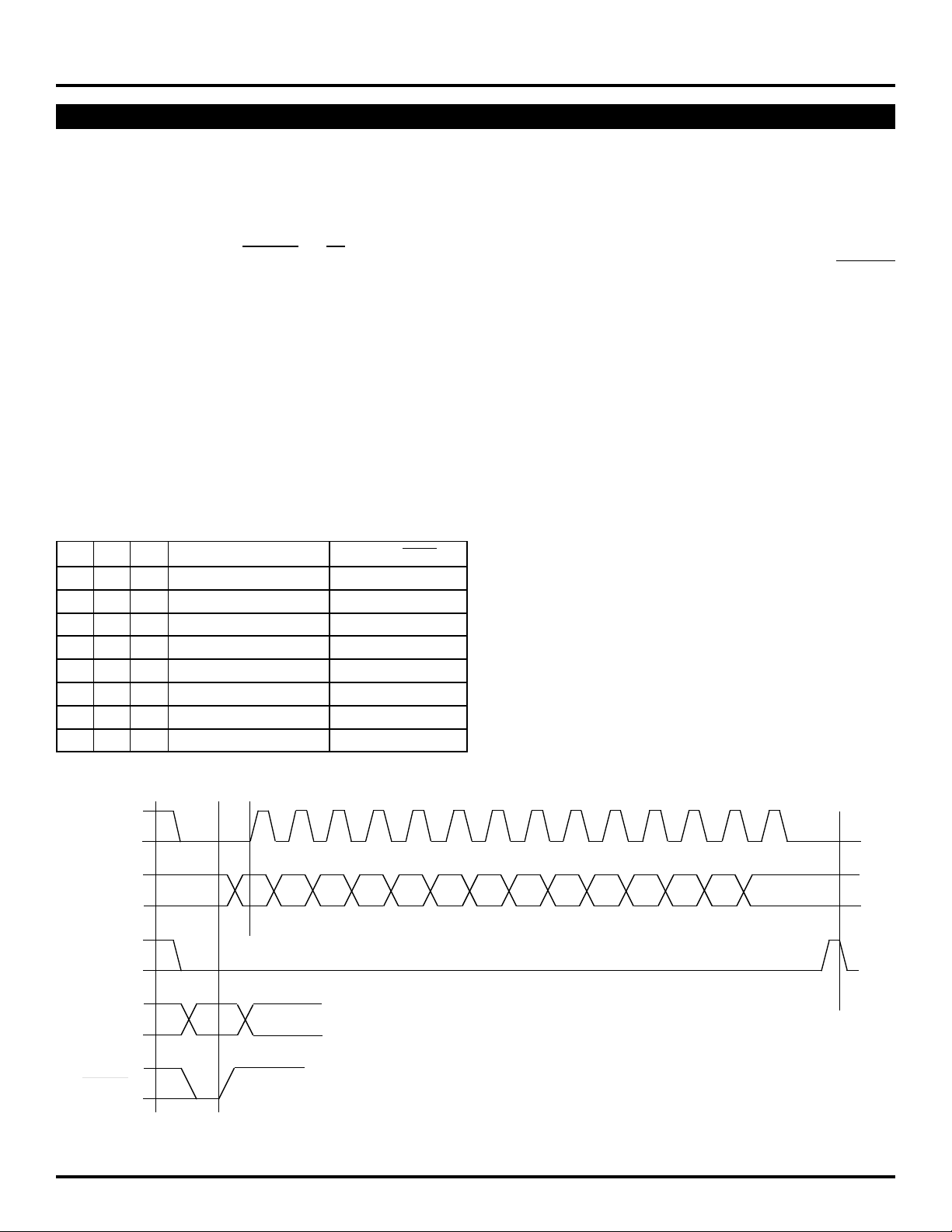
The Test register is loaded with the first three bits, the N
register with the next two and the M register with the final eight
bits of the data stream on the S_DATA input. For each register
the most significant bit is loaded first (T2, N1 and M8).
When T[2:0] is set to 100 the SY89429A is placed in PLL
bypass mode. In this mode the S_CLOCK input is fed directly
into the M and N dividers. The N divider drives the FOUT
differential pair and the M counter drives the TEST output pin.
In this mode the S_CLOCK input could be used for low speed
board level functional test or debug. Bypassing the PLL and
driving FOUT directly gives the user more control on the test
clocks sent through the clock tree (See detailed Block Diagram).
Because the S_CLOCK is a TTL level the input frequency is
limited to 250MHz or less. This means the fastest the FOUT
pin can be toggled via the S_CLOCK is 125MHz as the
minimum divide ratio of the N counter is 2. Note that the M
counter output on the TEST output will not be a 50% duty cycle
due to the way the divider is implemented.
S
_CLOCK
S
_DATA
S
_LOAD
M[8:0]
N[1:0]
P
_LOAD
T2 T1 T0 N1 N0 M8 M7 M6 M5 M4 M3 M2 M1 M0
First
Bit
M,N
Input S_DATA to M0 then M1, then M2, etc., as indicated above.
5
Last
Bit
Page 6
ClockWorks™
Micrel
SY89429A
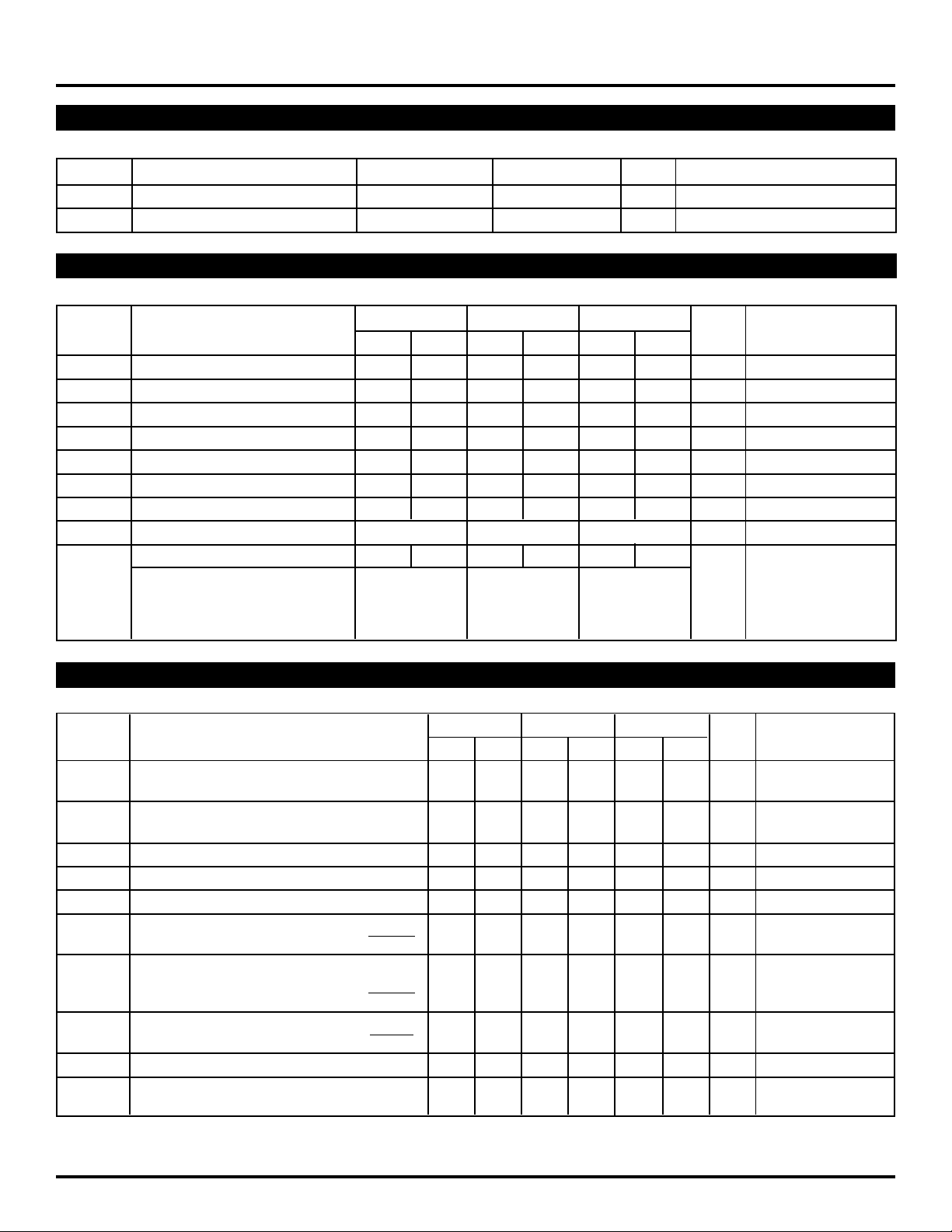
100H ECL DC ELECTRICAL CHARACTERISTICS
VCC1 = VCC_QUIET = VCC_TTL = +5.0V ±5%; VCC_OUT = +3.3V to +5.0V ±5%; TA = 0°C to +75°C
Symbol Parameter Min. Max. Unit Condition
VOH Output HIGH Voltage VCC_OUT –1.075 VCC_OUT –0.830 V 50Ω to VCC_OUT –2V
V
OL Output LOW Voltage VCC_OUT –1.860 VCC_OUT –1.570 V 50Ω to VCC_OUT –2V
TTL DC ELECTRICAL CHARACTERISTICS
VCC1 = VCC_QUIET = VCC_TTL = +5.0V ±5%; VCC_OUT = +3.3V to +5.0V ±5%; TA = 0°C to +75°C
A = 0°CTA = +25°CTA = +75°C
T
Symbol Parameter Min. Max. Min. Max. Min. Max. Unit Condition
VIH Input HIGH Voltage 2.0 — 2.0 — 2.0 — V —
VIL Input LOW Voltage — 0.8 — 0.8 — 0.8 V —
IIH Input HIGH Current — 50 — 50 — 50 µAVIN = 2.7V
IIL Input LOW Current —–0.6 —–0.6 —–0.6 mA VIN = 0.5V
VIK Input Clamp Voltage —–1.2 —–1.2 —–1.2 V IIN = –12mA
VOH Output HIGH Voltage — 2.5 — 2.5 — 2.5 V IOH = –2.0mA
VOL Output LOW Voltage — 0.5 — 0.5 — 0.5 V IOL = 8mA
IOS Output Short Circuit Current –80 (Typ.) –80 (Typ.) –80 (Typ.) mA VOUT = 0V
I
CC1 Supply Current — 225 — 225 — 225 mA —
Typical % of I
CC1 VCC1 91% 91% 91%
VCC_OUT 4.5% 4.5% 4.5%
VCC_QUIET 2.25% 2.25% 2.25%
VCC_TTL 2.25% 2.25% 2.25%
AC ELECTRICAL CHARACTERISTICS
VCC1 = VCC_QUIET = VCC_TTL = +5.0V ±5%; VCC_OUT = +3.3V to +5.0V ±5%; TA = 0°C to +75°C
TA = 0°CTA = +25°CTA = +75°C
Symbol Parameter Min. Max. Min. Max. Min. Max. Unit Condition
fMAXI Maximum Input Frequency
f
MAXO Maximum Output Frequency VCO (Internal) 400 800 400 800 400 800 MHz
tLOCK Maximum PLL Lock Time — 10 — 10 — 10 ms
tjitter Cycle-to-Cycle Jitter (Peak-toPeak) — ±25 — ±25 — ±25 ps Test output static
tS Setup Time S_DATA to S_CLOCK 20 — 20 — 20 — ns
H Hold Time S_DATA to S_CLOCK 20 — 20 — 20 — ns
t
pw(MIN) Minimum Pulse Width S_LOAD 50 — 50 — 50 — ns
t
tDC FOUT Duty Cycle 45 55 45 55 45 55 %
t
r Output Rise/Fall FOUT 300 800 300 800 300 800 ps
tf 20% to 80%
NOTE:
1. 10MHz is the maximum frequency to load the feedback divide registers. S_CLOCK can be switched at high frequencies when used as a test clock in
TEST_MODE 6.
(1)
S_CLOCK — 10 — 10 — 10 MHz Fundamental
Xtal Oscillator 10 25 10 25 10 25 Cyrstal
FOUT 25 400 25 400 25 400
S_
CLOCK to S_LOAD 20 — 20 — 20 —
M, N to P_LOAD 20 — 20 — 20 —
S_CLOCK to S_LOAD 20 — 20 — 20 —
M, N to P_LOAD 20 — 20 — 20 —
P_LOAD 50 — 50 — 50 —
6
Page 7
Micrel
D
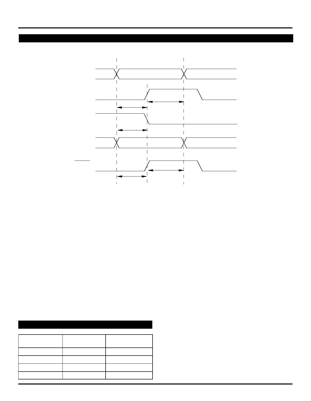
TIMING DIAGRAM
S_
S_
S_
P_
DATA
CLOCK
LOA
M[8:0]
N[1:0]
LOAD
t
SET-UP
t
SET-UP
t
HOLD
t
HOLD
ClockWorks™
SY89429A
PRODUCT ORDERING CODE
t
SET-UP
Ordering Package Operating
Code Type Range
SY89429AJC J28-1 Commercial
SY89429AJCTR J28-1 Commercial
SY89429AZC Z28-1 Commercial
SY89429AZCTR Z28-1 Commercial
7
Page 8
Micrel
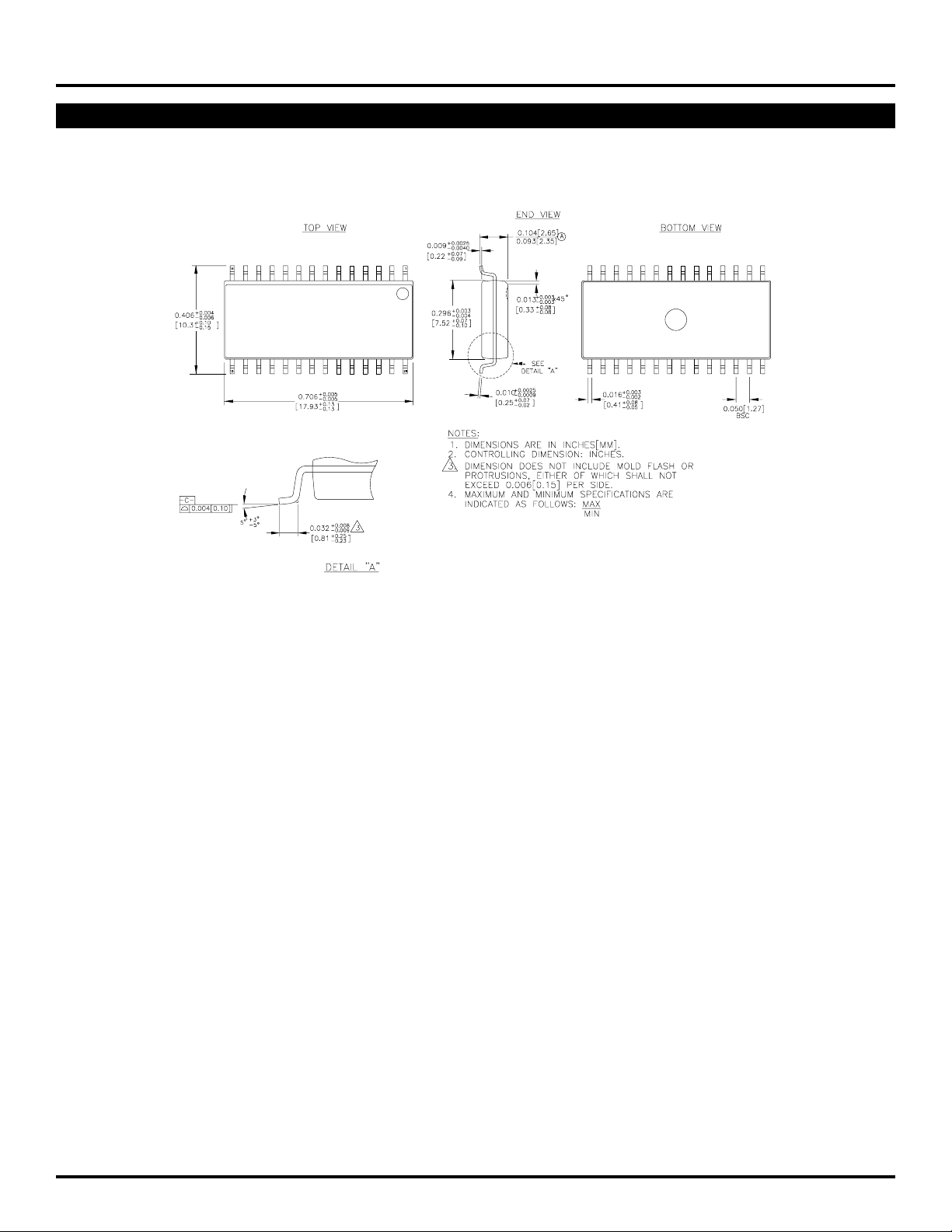
28 LEAD SOIC .300" WIDE (Z28-1)
ClockWorks™
SY89429A
Rev. 02
8
Page 9
Micrel
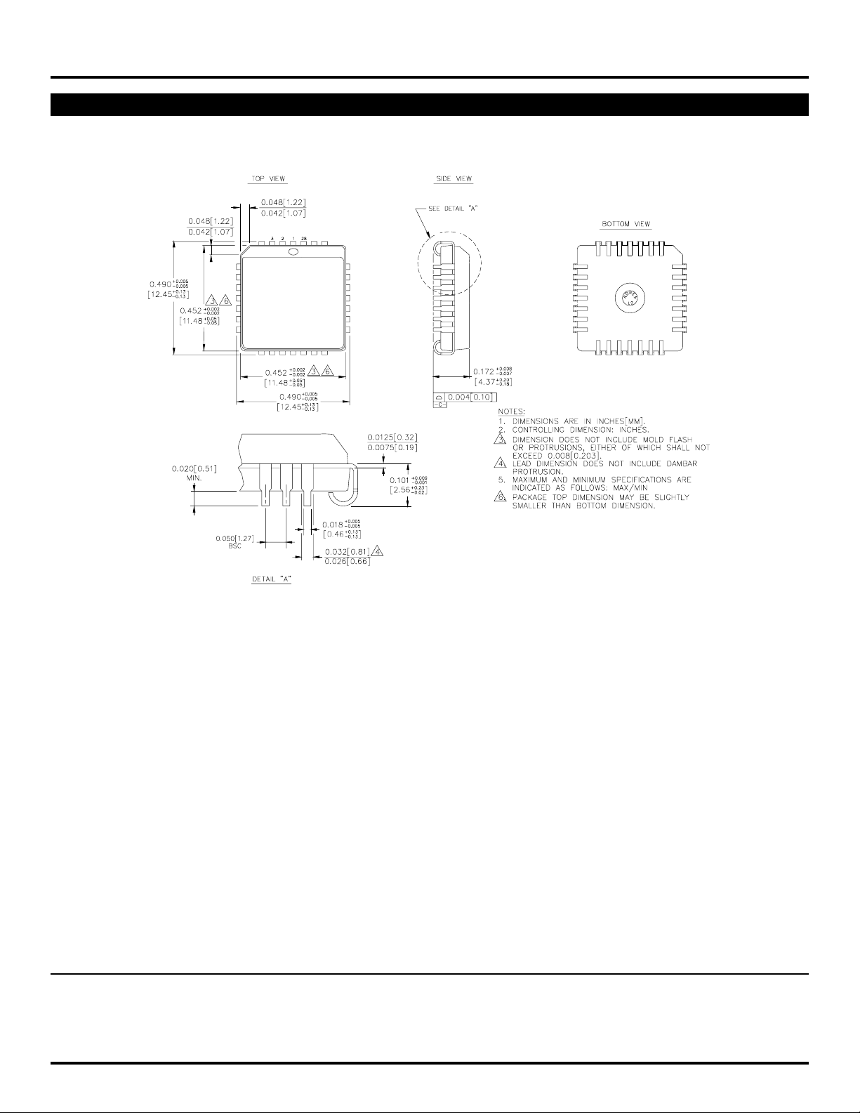
28 LEAD PLCC (J28-1)
ClockWorks™
SY89429A
Rev. 03
MICREL-SYNERGY 3250 SCOTT BOULEVARD SANTA CLARA CA 95054 USA
TEL + 1 (408) 980-9191 FAX + 1 (408) 914-7878 WEB http://www.micrel.com
This information is believed to be accurate and reliable, however no responsibility is assumed by Micrel for its use nor for any infringement of patents or
other rights of third parties resulting from its use. No license is granted by implication or otherwise under any patent or patent right of Micrel Inc.
© 2000 Micrel Incorporated
9
 Loading...