

Page 1
5V/3.3V DUAL
A
A
PHASE LOCKED LOOP
ClockWorks™
SY89420V
FEATURES
■ 3.3V and 5V power supply options
■ 1.12GHz maximum VCO frequency
■ 30MHz to 560MHz reference input operating
frequency
■ Frequency doubler mode
■ Low jitter design
■ PECL differential outputs
■ PECL and TTL reference voltages available
■ External loop filter optimizes performance/cost
■ Available in 28-pin PLCC package
APPLICATIONS
■ Workstations
■ Advanced communications
■ High-end consumer
■ High-performance computing
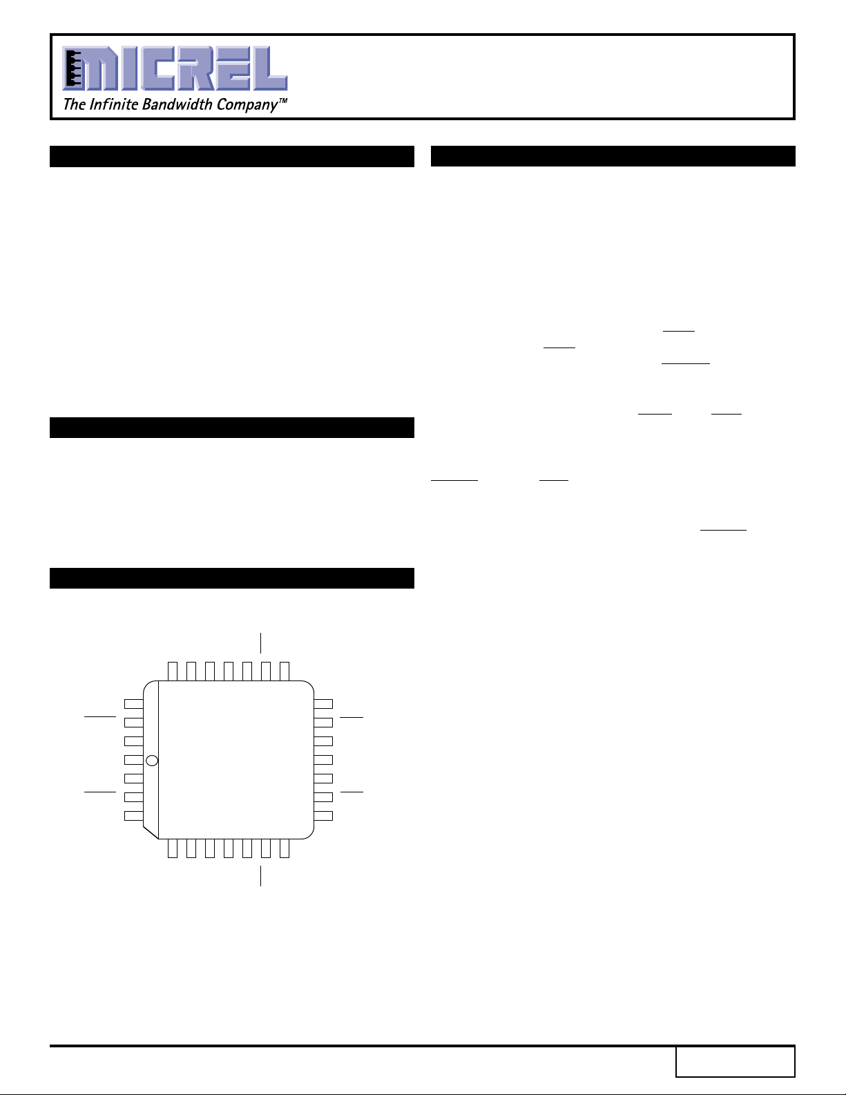
PIN CONFIGURATION
S3B
FINB
FINB
18
17
16
15
14
13
12
S4B
RINB
RINB
V
EE
RINA
RINA
V
BB
V
CCOB
FOUTB
FOUTB
V
CC
FOUT
FOUT
V
CCOA
S1B
F1B
F2B
S2B
24 23 22 21 20 19
25
26
27
28
1
2
3
4
TOP VIEW
PLCC
J28-1
567891011
DESCRIPTION
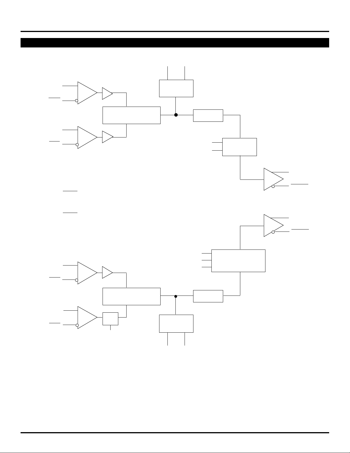
The SY89420V device consists of two identical, low
jitter, digital Phase Locked Loops based on Micrel-Synergy's
differential PLL technology. Each of the PLLs (PLLA and
PLLB) is capable of operating in the 30MHz to 560MHz
input reference frequency range independently of the other
and is configurable separately. The PLLs can be configured
to be matched in all regards, or can be configured so that
PLLB is used as a frequency doubler, while PLLA is used
to regenerate the undoubled frequency.
Two reference inputs (RINX and RINX), two feedback
inputs (FINX and FINX), two filter pins (F1X and F2X) and
two differential outputs (FOUTX and FOUTX) are provided
for each of the two PLLs. The reference and feedback
inputs can be used as either differential or single-ended
inputs. In single-ended mode RINX and FINX can be
connected to either V
VTH for normal TTL levels.
Feedback for the loops is realized by connecting FOUTX,
FOUTX to FINX, FINX by means of external circuitry. This
allows the user the flexibility of inserting additional circuitry
off-chip in the feedback paths, such as a divider. Pulldown
resistors are required for the FOUTX and FOUTX pins.
Use of a phase-frequency detector results in excellent
PLL locking and tracking characteristics. Error correction
voltages are generated by the detector if either phase or
frequency deviations occur. The VCO has a frequency
range covering more than a 2:1 ratio from 480MHz to
1120MHz.
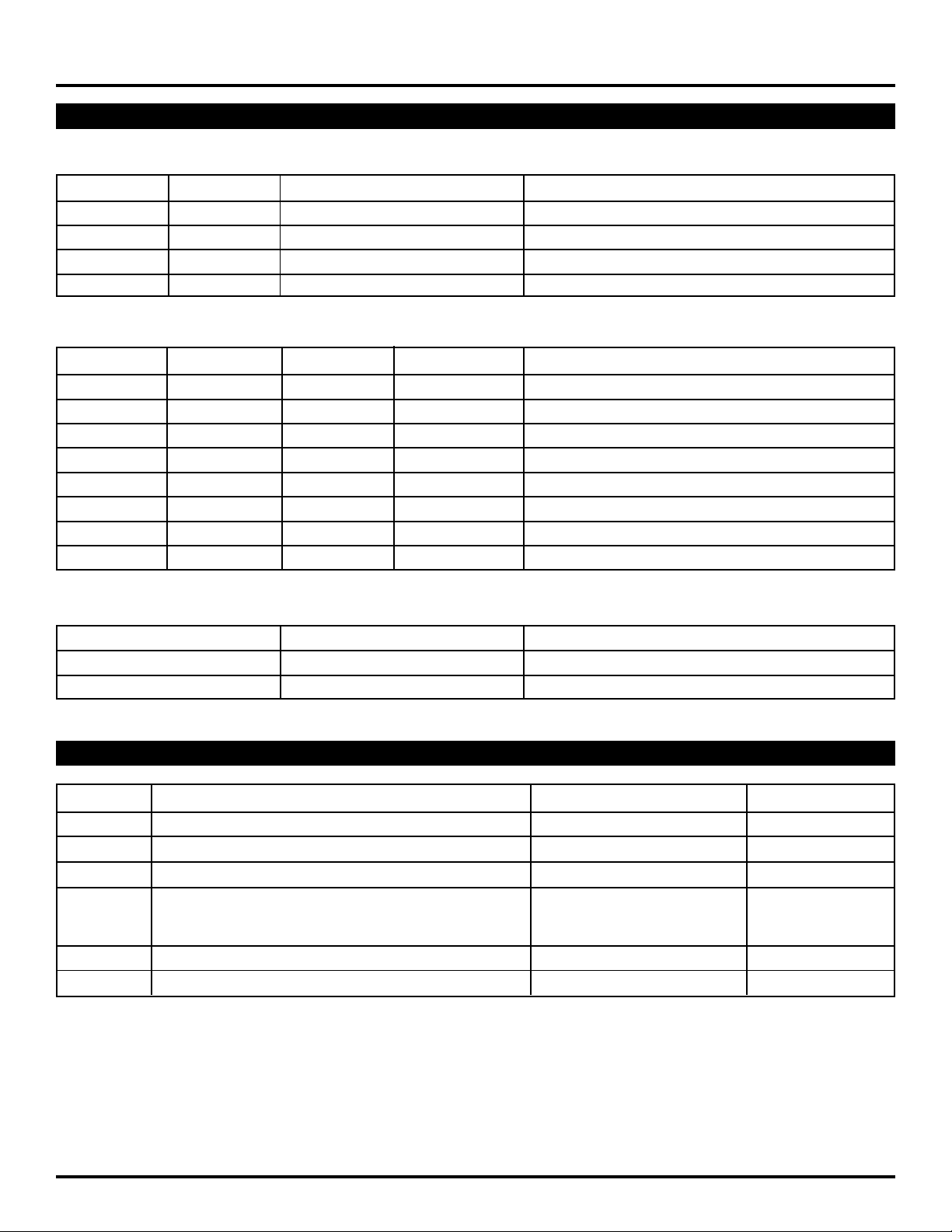
Select pins S1X and S2X are used to program the N
dividers for optimum VCO operation, in other words with
the VCO in the center of its range. Additional select pins,
S3B and S4B, are provided for PLLB. When both S3B and
S4B are low, PLLB is identical to PLLA. When S3B is high,
NB can be set to 1, 10, 18, or 20. When S4B is high, the
frequency doubler option is enabled (P = 2). All Select pins
are TTL compatible.
BB for normal 100K PECL levels or
TH
F1A
F2A
V
FINA
FINA
Rev.: K Amendment: /0
1
Issue Date: May 2000
S1A
S2A
Page 2
Micrel
BLOCK DIAGRAM
ClockWorks™
SY89420V
F1A F2A
RINA
RINA
FINA
FINA
V
BB
V
TH
D
PHASE-FREQUENCY
DETECTOR
D
LOOP
FILTER
VCO
S1A
S2A
÷ N
A
(2, 4, 8, 16)
FOUTA
FOUTA
FOUTB
FOUTB
RINB
RINB
FINB
FINB
D
PHASE-FREQUENCY
DETECTOR
÷
P
(1, 2)
S4B
LOOP
FILTER
F1B F2B
S1B
S2B
S3B
÷ N
(1,2,4,8,10,12,16,20)
VCO
B
2
Page 3
Micrel
ClockWorks™
SY89420V
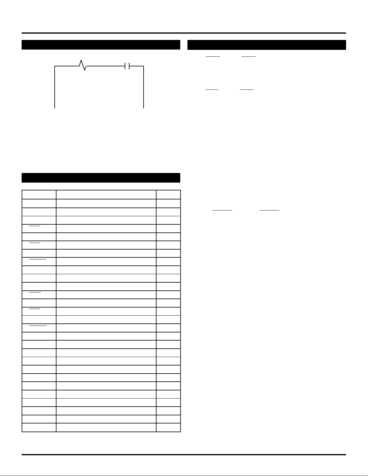
LOOP FILTER COMPONENT SELECTION
R
F1X
C = 1.0µF ±10% (X7R dielectric)
R = 560Ω ±10%
C
F2X
PIN NAMES
Pin Function I/O
F1A Filter Pin 1A I/O
F2A Filter Pin 2A I/O
RINA Reference Input A I
RINA Inverted Reference Input A I
FINA Feedback Input A I
FINA Inverted Feedback Input A I
FOUTA Frequency Output A O
FOUTA Inverted Frequency Output A O
F1B Filter Pin 1B I/O
F2B Filter Pin 2B I/O
RINB Reference Input B I
RINB Inverted Reference Input B I
FINB Feedback Input B I
FINB Inverted Feedback Input B I
FOUTB Frequency Output B O
FOUTB Inverted Frequency Output B O
VCC VCC —
VCCOA Output A VCC —
VCCOB Output B VCC —
VEE VEE (0V) —
VBB PECL Threshold Voltage O
VTH TTL Threshold Voltage O
S1A Select Input 1A (TTL) I
S2A Select Input 2A (TTL) I
S1B Select Input 1B (TTL) I
S2B Select Input 2B (TTL) I
S3B Select Input 3B (TTL) I
S4B Select Input 4B (TTL) I
PIN DESCRIPTION
RINA, RINA, RINB, RINB
Reference frequency inputs for loop A and B. These are
differential signal pairs and may be driven differentially or
single-ended.
FINA, FINA, FINB, FINB
Feedback frequency inputs for loop A and B. These are
differential signal pairs and may be driven differentially or
single-ended.
V
BB, VTH
These are the reference voltages for use as bias for the
frequency inputs. The references are generated on-chip. VBB
is PECL compatible, while VTH is TTL compatible.
F1A, F2A, F1B, F2B
These pins are connection points for the loop filters, which are
to be provided off-chip. F1X is the high impedance side, F2X
is the reference side. The loop filter should be a first order, low
pass with a DC block. The difference voltage on these pins will
be a DC level, which is controlled by the loop feedback and
determined by the required VCO frequency.
FOUTA, FOUTA, FOUTB, FOUTB
Frequency outputs for the loops. These are differential,
positive referenced, emitter-follower signals and must be
terminated off-chip. Termination in 50 ohms is recommended.
S1A, S2A, S1B, S2B, S3B, S4B
These inputs are used to select the configuration for PLLA and
PLLB. They are compatible with standard TTL signal levels.
See the Frequency Selection Table for details of the logic.
VCC
This is the positive supply for the entire chip excluding output
buffers. It should be decoupled and present a very low
impedance in order to assure low-jitter operation.
VCCOA, VCCOB
These are the positive supplies for the output buffers. They
are constrained to be equal to the value of VCC. They should
be decoupled and present a very low impedance in order to
assure low-jitter operation.
VEE
This pin is the negative supply for the chip and is normally
connected to ground (0V).
3
Page 4
Micrel
FREQUENCY SELECTION TABLE
PLLA
S2A S1A Divide-by-N Output Frequency Range (MHz)
0 0 N = 2 240 – 560
0 1 N = 4 120 – 280
1 0 N = 8 60 – 140
1 1 N = 16 30 – 70
PLLB
S3B S2B S1B Divide-by-N Output Frequency Range (MHz)
0 0 0 N =2 240 – 560
0 0 1 N = 4 120 – 280
0 1 0 N = 8 60 – 140
0 1 1 N = 16 30– 70
1 0 0 N = 1 480 – 1120
1 0 1 N = 10 48 – 112
1 1 0 N = 12 40 – 93.3
1 1 1 N = 20 24 – 56
ClockWorks™
SY89420V
S4B Divide-by-P Max. Feedback Frequency (MHz)
0 P =1 560
1 P = 2 1120
ABSOLUTE MAXIMUM RATINGS
(1)
Symbol Parameter Value Unit
VCC Power Supply Voltage –0.5 to +7.0 V
VI TTL Input Voltage
II TTL Input Current
OUT ECL Output Current mA
I
(2)
(2)
–0.5 to 6.0 V
–30 to +5.0 mA
— Continuous 50
— Surge 100
Tstore Storage Temperature –65 to +150 °C
TA Operating Temperature Range
NOTES:
1. Permanent device damage may occur if ABSOLUTE MAXIMUM RATINGS are exceeded. This is a stress rating only and functional operation is not
implied at conditions other than those detailed in the operational sections of this data sheet. Exposure to ABSOLUTE MAXIMUM RATING conditions
for extended periods may affect device reliability.
2. Either voltage limit or current limit is sufficient to protect input.
3. All DC and AC electrical characteristics are specified over the operating temperature range.
(3)
0 to +85 °C
4
Page 5
Micrel
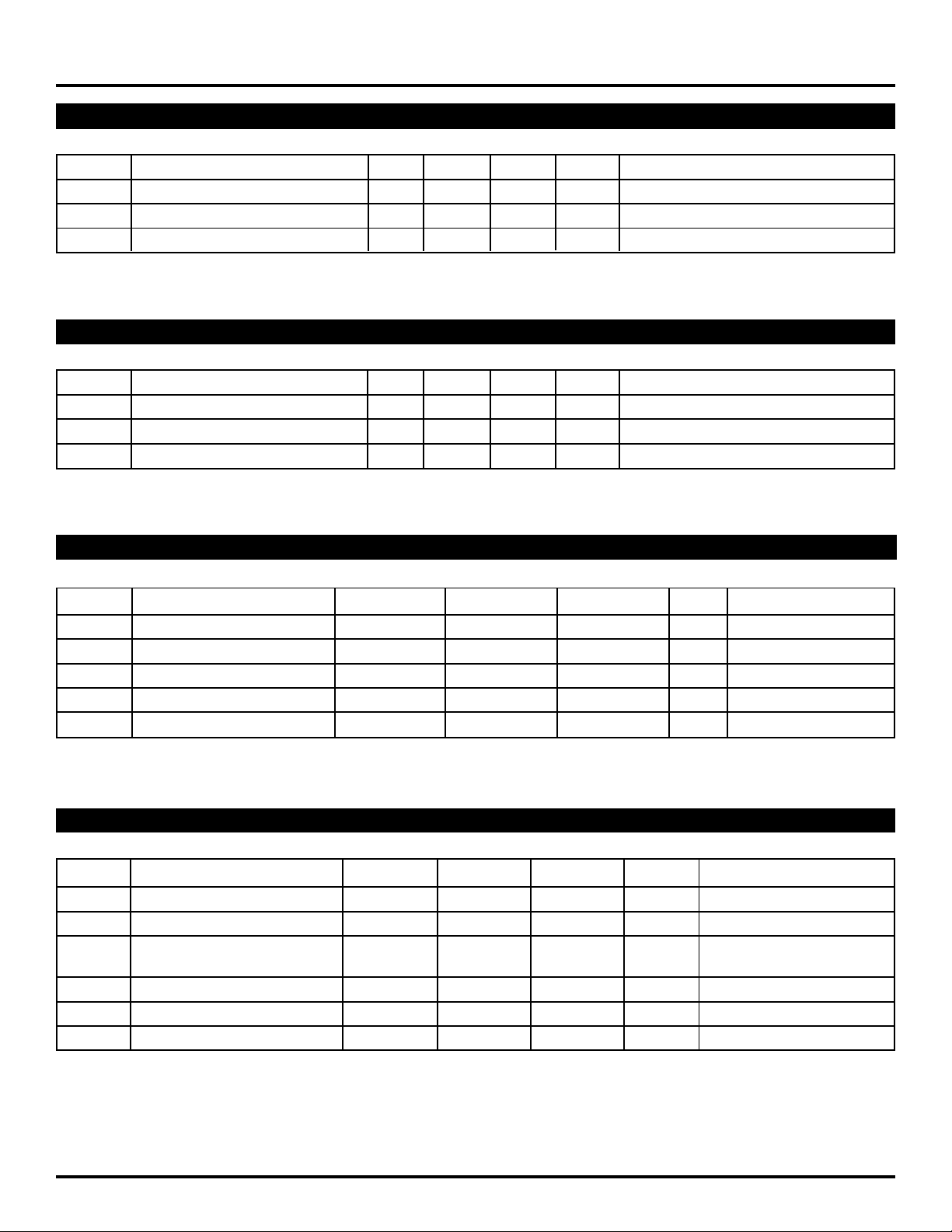
5V DC ELECTRICAL CHARACTERISTICS
VCC = VCCOA = VCCOB = 5.0V ±5%
Symbol Parameter Min. Typ. Max. Unit Condition
VCC Power Supply Voltage 4.75 — 5.25 V VCC = VCCO
ICC Power Supply Current (VCC) ——200 mA
CCO Power Supply Current (VCCO) ——28 mA PECL outputs are open
I
3.3V DC ELECTRICAL CHARACTERISTICS
VCC = VCCOA = VCCOB = 3.3V ±5%
Symbol Parameter Min. Typ. Max. Unit Condition
VCC Power Supply Voltage 3.135 — 3.465 V VCC = VCCO
ICC Power Supply Current (VCC) ——200 mA
CCO Power Supply Current (VCCO) ——28 mA PECL outputs are open
I
ClockWorks™
SY89420V
PECL DC ELECTRICAL CHARACTERISTICS
VCC = VCCOA = VCCOB = 3.3V or 5.0V ±5%
Symbol Parameter Min. Typ. Max. Unit Condition
VOH Output HIGH Voltage VCC – 1.025 — VCC – 0.780 V
VOL Output LOW Voltage VCC – 1.810 — VCC – 1.520 V
VIH Input HIGH Voltage VCC – 1.165 — VCC – 0.780 V
VIL Input LOW Voltage VCC – 1.810 — VCC – 1.475 V
BB PECL Threshold — VCC – 1.35 — V
V
TTL DC ELECTRICAL CHARACTERISTICS
VCC = VCCOA = VCCOB = 3.3V or 5.0V ±5%
Symbol Parameter Min. Typ. Max. Unit Condition
VIH Input HIGH Voltage 2.0 ——V
VIL Input LOW Voltage ——0.8 V
I
IH Input HIGH Current ——20 µAVIN = 2.7V
100 VIN = VCC
IIL Input LOW Current ——–0.3 mA VIN = 0.5V
VIK Input Clamp Voltage ——– 1.2 V IIN = –12mA
TH TTL Threshold — 1.5 — V
V
5
Page 6
Micrel
z
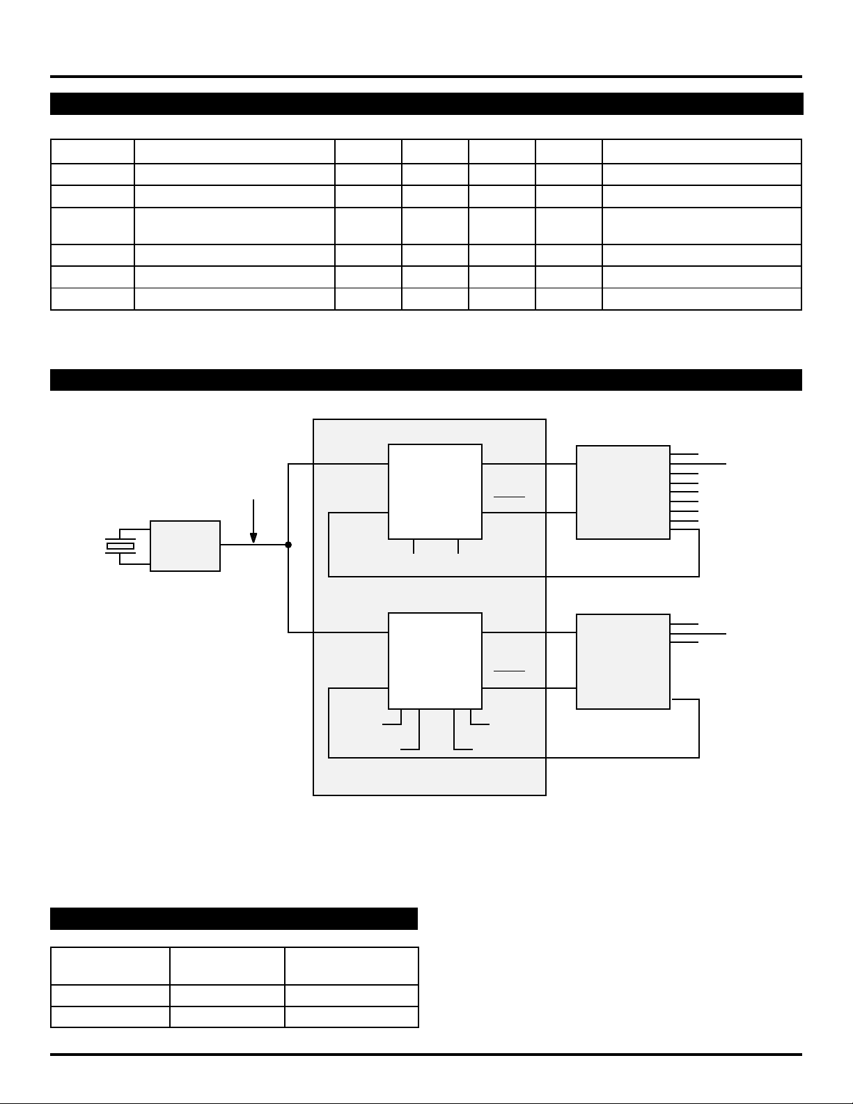
AC ELECTRICAL CHARACTERISTICS
VCC = VCCOA = VCCOB = 3.3V or 5.0V ± 5%
Symbol Parameter Min. Typ. Max. Unit Condition
∆Τ Output Period Jitter — 10 15 ps rms
PPW Output Duty Cycle 45 50 55 %
tr Output Rise/Fall Time — 300 550 ps —
tf (20% to 80%) — 300 550
FOUTA Output Frequency PLLA ——560 MHz
FOUTB Output Frequency PLLB ——1120 MHz S4B=1
RINA, B Input Frequency PLLA, B ——560 MHz
APPLICATION
ClockWorks™
SY89420V
16MH
SY89429A
RINA
50MHz
Clock
FINA
RINB
FINB
S4B = 1
S3B = 1 S2B = 0
50MHz Low Skew Clock System with 100MHz Clock to CPU
PLLA
S2A = 1 S1A = 1
PLLB
SY89420V
OUTA
OUTA
OUTB
OUTB
S1B = 1
50MHz
SY100H641
100MHz
SY100H842
PRODUCT ORDERING CODE
Ordering Package Operating
Code Type Range
SY89420VJC J28-1 Commercial
SY89420VJCTR J28-1 Commercial
6
Page 7
Micrel
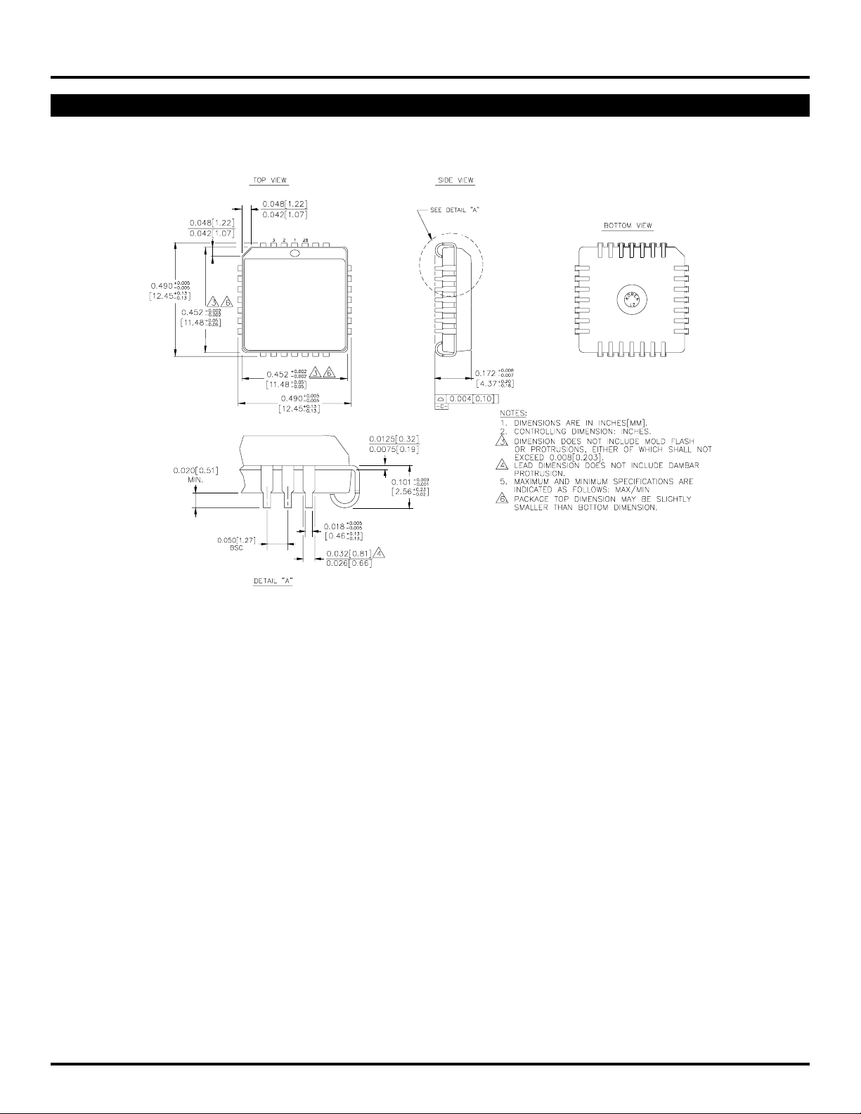
28 LEAD PLCC (J28-1)
ClockWorks™
SY89420V
Rev. 03
7
Page 8

Micrel
ClockWorks™
SY89420V
MICREL-SYNERGY 3250 SCOTT BOULEVARD SANTA CLARA CA 95054 USA
TEL + 1 (408) 980-9191 FAX + 1 (408) 914-7878 WEB http://www.micrel.com
This information is believed to be accurate and reliable, however no responsibility is assumed by Micrel for its use nor for any infringement of patents or
other rights of third parties resulting from its use. No license is granted by implication or otherwise under any patent or patent right of Micrel Inc.
© 2000 Micrel Incorporated
8
 Loading...