

Page 1
5V/3.3V 2.5Gbps
Limiting
Amplifer
ECL
Buffer
GND
Enable
Level
Detect
EN
SD
D
OUT
/D
OUT
D
IN
/D
IN
V
REF
V
CC
SD
LVL
LIMITING POST AMPLIFIER
WITH SIGNAL DETECT
SY88943V
FEATURES
■ 3.3V and 5V power supply options
■ Up to 2.5Gbps operation
■ Low noise
■ Chatter-fee signal detect (SD) generation
■ Open collector TTL signal detect (SD) output
■ TTL EN input
■ Differential PECL inputs for data
■ Single power supply
■ Designed for use with Micrel-Synergy laser diode
driver and controller
■ Available in a tiny (3mm) 10-pin MSOP
PIN CONFIGURATION
DIN
/DIN
VREF
SDLVL
1EN
2
MSOP
3
K10-1
4
5
10 VCC
DOUT
9
/DOUT
8
SD
7
GND
6
DESCRIPTION
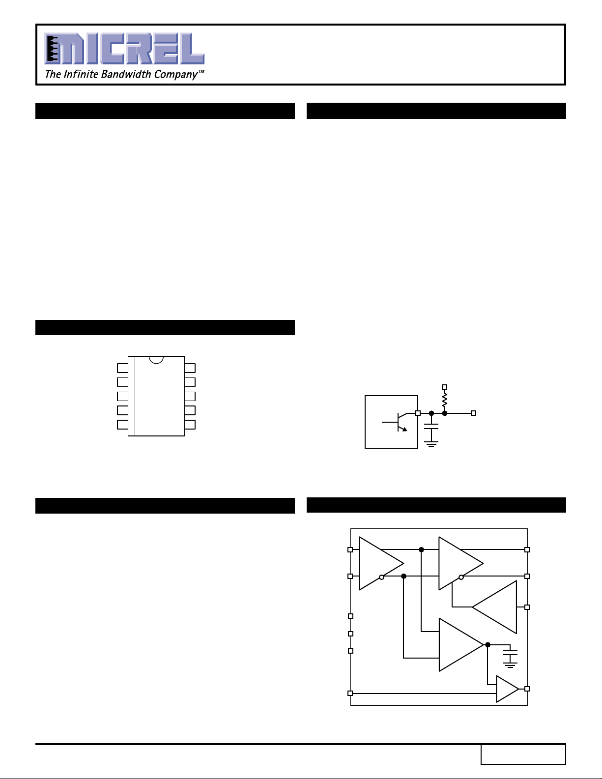
The SY88943V limiting post amplifier with its high gain
and wide bandwidth is ideal for use as a post amplifier in
fiber-optic receivers with data rates up to 2.5Gbps.
Signals as small as 5mVp-p can be amplified to drive
devices with PECL inputs. The SY88943V generates a
chatter-free Signal Detect (SD) open collector TTL output.
The SY88943V incorporates a programmable level detect
function to identify when the input signal has been lost.
The SD output will change from logic “HIGH” to logic “LOW”
when input signal is smaller than the swing set by SD
This information can be fed back to the EN input of the
device to maintain stability under loss of signal condition.
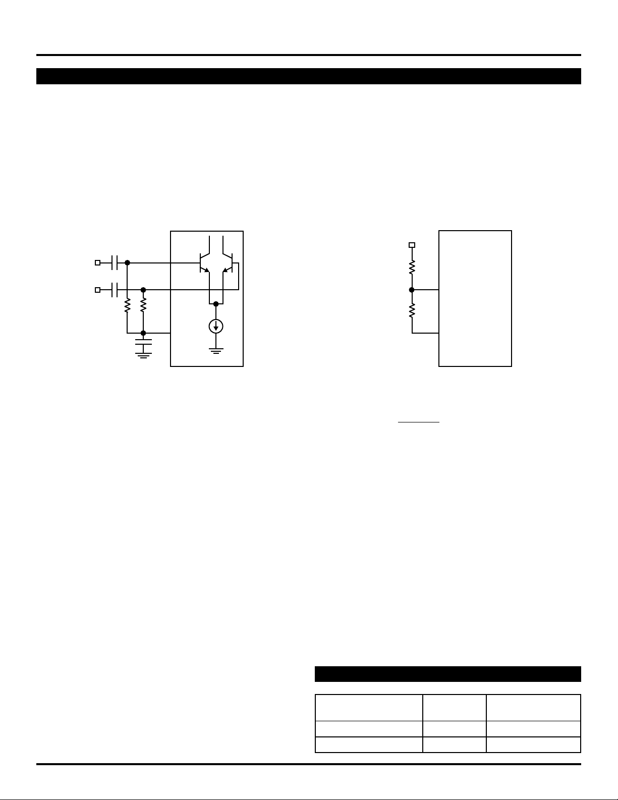
Using SD
be adjusted. The SD
a resistor divider between VCC and V
pin, the sensitivity of the level detection can
LVL
voltage can be set by connecting
LVL
as shown in Figure
REF
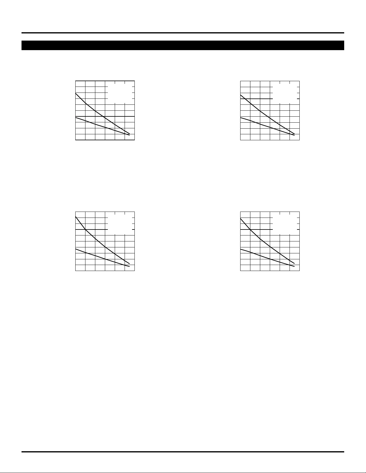
3. Figure 4, 5, 6, and 7 show the relationship between
input level sensitivity and the voltage set on SD
LVL
The SD output is a TTL open collector output that
requires a pull-up resistor for proper operation, Figure 1.
V
SY88943V
SD
CC
4.7kΩ to 10kΩ
LVL
.
.
APPLICATIONS
■ 1.25Gbps and 2.5Gbps ethernet
■ 531Mbps, 1062Mbps and 2.12Gbps Fibre Channel
■ 622Mbps SONET
■ Gigabit interface converter
■ 2.5Gbps SDH/SONET
■ 2.5Gbps proprietary links
Figure 1. SD Output with Desired Rise Time
BLOCK DIAGRAM
1
Rev.: B Amendment: /0
Issue Date: August 2000
Page 2
Micrel
SY88943V
PIN NAMES
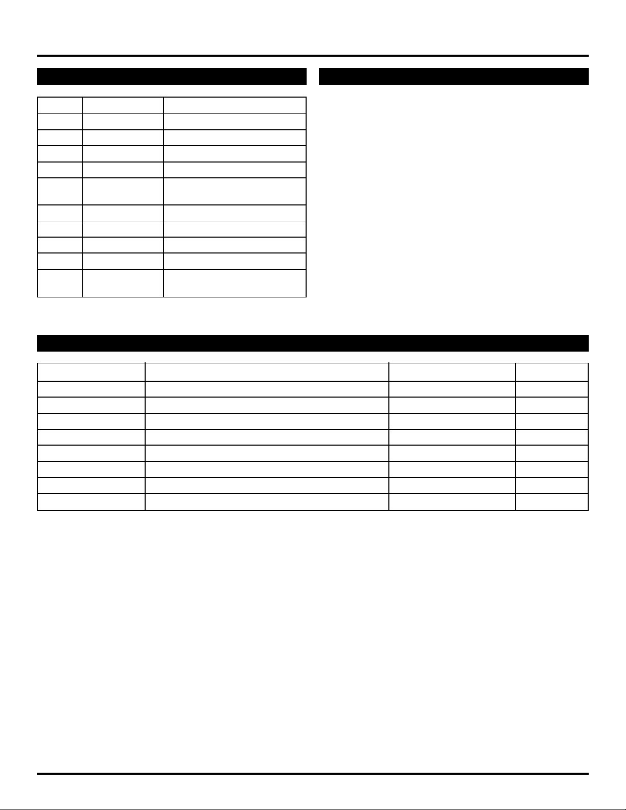
Pin Type Function
D
IN
/D
IN
SD
LVL
EN TTL Input Output Enable (Active High)
SD TTL Output Signal Detect
GND Ground Ground
/D
OUT
D
OUT
V
CC
V
REF
ABSOLUTE MAXIMUM RATINGS
Data Input Data Input
Data Input Inverting Data Input
Input SD Level Set
(Open Collector)
PECL Output Inverting Data Output
PECL Output Data Output
Power Supply Positive Power Supply
Output Reference Voltage Output for
SD Level Set (see Fig. 3)
(1)
GENERAL DESCRIPTION
General
The SY88943V is an integrated limiting amplifier intended
for high-frequency fiber-optic applications. The circuit
connects to typical transimpedance amplifiers found within
a fiber-optics link. The linear signal output from a
transimpedance amplifier can contain significant amounts
of noise, and may vary in amplitude over time. The
SY88943V limiting amplifier quantizes the signal and outputs
a voltage-limited waveform.
The EN pin allows the user to disable the output signal
without removing the input signal.
Symbol Rating Value Unit
V
CC
DIN, /D
IN
D
, /D
OUT
OUT
EN Input Voltage 0 to V
SD
LVL
V
REF
T
A
T
store
NOTE:
1. Permanent device damage may occur if ABSOLUTE MAXIMUM RATINGS are exceeded. This is a stress rating only and functional operation is not implied
at conditions other than those detailed in the operational sections of this data sheet. Exposure to ABSOLUTE MAXIMUM RATlNG conditions for extended
periods may affect device reliability.
Power Supply Voltage 0 to +7.0 V
Input Voltage 0 to V
CC
V
Output Voltage (with 50Ω load) VCC –2.5 to VCC +0.3 V
CC
Input Voltage 0 to V
CC
Output Voltage VCC –2.0 to V
CC
V
V
V
Operating Temperature Range –40 to +85 °C
Storage Temperature Range –55 to +125 °C
2
Page 3
Micrel
SY88943V
DC ELECTRICAL CHARACTERISTICS
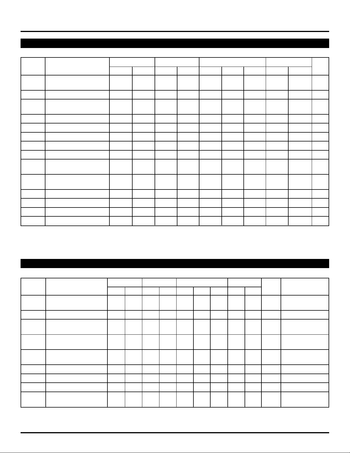
VCC = +5V ±10%, R
Symbol Parameter Min. Max. Min. Max. Min. Typ. Max. Min. Max. Unit
I
CC
I
IL
I
IH
V
CMR
V
offset
SD
V
OL
I
OH
V
OH
V
OL
V
REF
I
REF
V
IH
V
IL
NOTES:
1. No output load
2. IOL = + 2mA
3. VOH = 5.5V
Power Supply
(1)
Current
EN Input LOW Current
EN Input HIGH Current
Common Mode Range
Differential Output Offset — ±100 — ±100 — ±17 ±100 — ±100 mV
SD
LVL
Level V
LVL
SD Output Low Level
SD Output Leakage
D
and /D
OUT
HIGH Output
D
and /D
OUT
LOW Output
Reference Supply
V
Output Current –0.8 0.5 –0.8 0.5 –0.8 — 0.5 –0.8 0.5 mA
REF
EN Input HIGH Voltage
EN Input LOW Voltage
= 50Ω to VCC–2V
LOAD
5V — 40 — 40 — 33 40 — 45 mA
3.3V — 40 — 40 — 28 40 — 45
(2)
(3)
OUT
OUT
= –40°CT
T
A
(6)
–0.3
— 20
— 100
GND +2.0
REF
—–0.3
(4)
(5)
V
GND +2.0
CC
V
CC
= 0°CT
A
(6)
— 20
— 100
V
REF
—–0.3
(4)
(5)
V
CC
V
CC
(6)
——20
——100
GND +2.0
V
REF
= +25°CT
A
——–0.3
(4)
(5)
— V
— V
CC
CC
= +85°C
A
(6)
— 20
— 100
GND +2.0
V
REF
— mA
V
CC
V
CC
(4)
(5)
— 0.5 — 0.5 ——0.5 — 0.5 V
— 100 — 100 ——100 — 100 µA
VCC -1085 VCC -880 VCC -1025 VCC -880 VCC -1025 VCC -955 VCC -880 VCC -1025 VCC -880
VCC -1830 VCC -1555 VCC -1810 VCC -1620 VCC -1810 VCC -1705 VCC -1620 VCC -1810 VCC- 1620
VCC -1.38 VCC -1.26 VCC -1.38 VCC -1.26 VCC -1.38 VCC -1.32 VCC -1.26 VCC -1.38 VCC -1.26
2.0 — 2.0 — 2.0 ——2.0 — V
— 0.8 — 0.8 ——0.8 — 0.8 V
4. VIN = 2.7V
5. VIN = V
6. VIN = 0.5V
CC
µA
V
V
mV
mV
V
AC ELECTRICAL CHARACTERISTICS
VCC = +5V ±10%, R
Symbol Parameter Min. Max. Min. Max. Min. Typ. Max. Min. Max. Unit Conditions
PSRR Power Supply
Rejection Ratio 55MHz
V
ID
V
OD
t
ONL
t
ONH
t
OFFL
V
SR
HYS SD Hysteresis 2 8 2 8 2 4.6 8 2 8 dB 223-1 pattern
, t
t
r
f
NOTES:
1. Input referred noise = RMS output noise/low frequency gain.
2. Input is a 622MHz square wave.
Input Voltage Range 5 1800 5 1800 5 — 1800 5 1800 mVp-p
Differential Output —————700 ———mV VID = 15mVp-p
Voltage Swing
SD Release Time
Minimum Input
SD Release Time
Maximum Input
SD Assert Time
SD Sensitivity Range 5 50 5 50 5 — 50 5 50 MVp-p 223-1 pattern
Output Rise/Fall Time — 175 — 175 — 150 175 — 175 ps VID > 100mVp-p
= 50Ω to VCC–2V
LOAD
(1)
(2)
(3)
(4)
(3)
TA = –40°CTA = 0°CTA = +25°CTA = +85°C
—————35 ———dB Input referred,
—————300 ———mV VID = 5mVp-p
— 0.5 — 0.5 — 0.2 0.5 — 0.5 µs
— 0.5 — 0.5 — 0.2 0.5 — 0.5 µs
— 0.5 — 0.5 — 0.1 0.5 — 0.5 µs
—————t
3. Input is a 200MHz square wave, tr < 300ps, 8mVp-p.
4. Input is a 200MHz square wave, tr < 300ps, 1.8Vp-p.
rin,tfin
——— VID < 100mVp-p
3
Page 4
Micrel
DESIGN PROCEDURE
SY88943V
Output Termination
The SY88943V outputs must be terminated with a 50Ω
load to VCC–2V (or Thevenin equivalent).
Layout and PCB Design
Since the SY88943V is a high-frequency component,
performance can be largely determined by the board layout
and design. A common problem with high-gain amplifiers is
the feedback from the large swing outputs to the input via
the power supply.
0.1µF
0.1µF
0.1µF
Figure 2. Differential Input Configuration
D
IN+
D
IN–
50Ω50Ω
V
REF
The SY88943V ground pin should be connected to the
circuit board ground. Use multiple PCB vias close to the
part to connect to ground. Avoid long, inductive runs which
can degrade performance.
V
CC
R1
SD
LVL
R2
V
REF
NOTES:
SD
= VCC -1.32V +
LVL
R1 + R2 ≥ 2.6kΩ
Figure 3. SD
R2 × 1.32V
R1 + R2
LVL
Circuit
PRODUCT ORDERING CODE
Ordering Package Operating
Code Type Range
SY88943VKC K10-1 Commercial
SY88943VKCTR K10-1 Commercial
4
Page 5
Micrel
PERFORMANCE CURVE
SY88943V
SD Assert and Deassert Levels
vs SD
100
90
80
70
60
50
40
30
20
INPUT LEVEL (mVp-p)
10
0
0 -0.2 -0.4 -0.6 -0.8 -1.0 -1.2
SD
LVL
= VCC– V (V)
LVL
3.3V
T
= 25°C
A
2.5Gbps
Pattern 2
Figure 4.
SD Assert and Deassert Levels
vs SD
100
90
80
70
60
50
40
30
20
INPUT LEVEL (mVp-p)
10
0
0 -0.2 -0.4 -0.6 -0.8 -1.0 -1.2
SD
LVL
= VCC– V (V)
LVL
3.3V
T
= 25°C
A
2.5Gbps
Pattern 2
SD Assert and Deassert Levels
vs SD
100
90
80
23
-1
70
60
50
40
30
20
INPUT LEVEL (mVp-p)
10
0
0 -0.2 -0.4 -0.6 -0.8 -1.0 -1.2
SD
LVL
5.0V
T
2.5Gbps
Pattern 2
= VCC– V (V)
LVL
= 25°C
A
23
-1
Figure 5.
SD Assert and Deassert Levels
vs SD
100
90
80
7
-1
70
60
50
40
30
20
INPUT LEVEL (mVp-p)
10
0
0 -0.2 -0.4 -0.6 -0.8 -1.0 -1.2
SD
LVL
5.0V
T
2.5Gbps
Pattern 2
= VCC– V (V)
LVL
= 25°C
A
7
-1
Figure 6.
Figure 7.
5
Page 6
Micrel
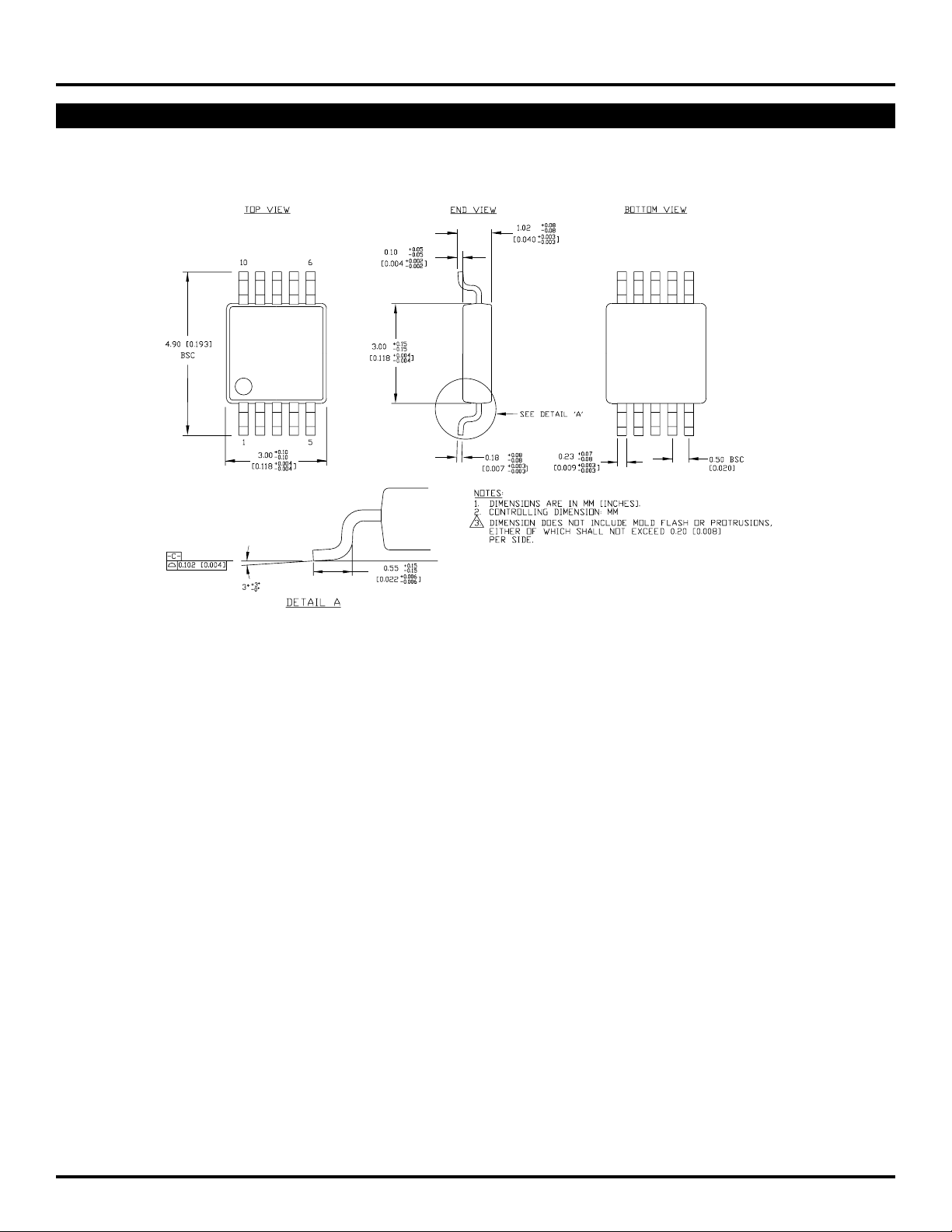
10 LEAD MSOP (K10-1)
SY88943V
Rev. 00
6
Page 7

Micrel
SY88943V
7
Page 8

Micrel
SY88943V
MICREL-SYNERGY 3250 SCOTT BOULEVARD SANTA CLARA CA 95054 USA
TEL + 1 (408) 980-9191 FAX + 1 (408) 914-7878 WEB http://www.micrel.com
This information is believed to be accurate and reliable, however no responsibility is assumed by Micrel for its use nor for any infringement of patents or
other rights of third parties resulting from its use. No license is granted by implication or otherwise under any patent or patent right of Micrel Inc.
© 2000 Micrel Incorporated
8
 Loading...