

Page 1
SDH/SONET 2.5Gbps
LASER DIODE DRIVER
SY88922
FEATURES
■ Up to 2.5Gbps operation
■ 25mA peak drive current
■ Separate modulation control
■ Separate output enable for laser safety
■ Differential inputs for data
■ 75KΩ input pulldown resistor
■ Designed for use with SY88923, SY88904 or SY88905
■ Available in a tiny 10-pin (3mm) MSOP
PIN CONFIGURATIONS
1/EN
D
IN
2
/D
IN
V
REF
R
SET
MSOP
3
K10-1
4
5
10 V
9
8
7
6
CC
OUT
/OUT
GND
GND
DESCRIPTION
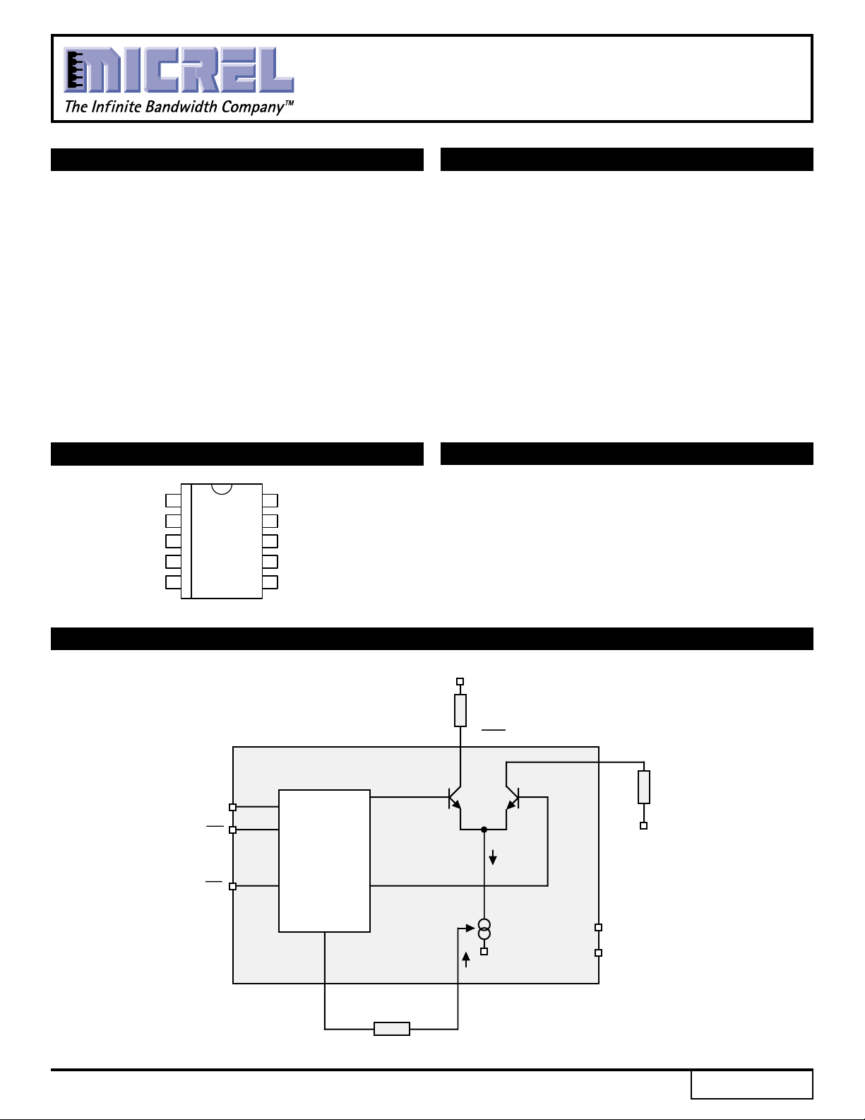
The SY88922 is a high-speed current switch for driving
a semiconductor laser diode in optical transmission
applications. The output current, or modulation current
IMOD, is DC current controlled by IRSET, current through
the resistor RSET. The output OUT is HIGH when output
enable is HIGH.
The device incorporates complementary open collector
outputs with a capability of driving peak current of 25mA.
The resistor REXT must be placed between /OUT and
VCC to dissipate the worst case power. RSER is
recommended to compensate for laser diode matching
issues.
The SY88922 utilizes the high performance bipolar
ASSET™ technology.
APPLICATIONS
■ 1.25Gbps Gigabit Ethernet
■ 531Mbps and 1062Mbps Fibre Channel
■ 622Mbps SONET
■ Gigabit Interface Converter
■ 2.5Gb/s SDH/SONET
BLOCK DIAGRAM
D
D
EN
V
CC
R
EXT
OUT
OUT
R
SER
IN
IN
Internal Logic
I
MOD
to Laser Diode
BIAS
Control
Modulation Control
40X
CC
V
GND
GND
SET
V
REF
R
R
SET
1
Rev.: B Amendment: /1
Issue Date: July 2000
Page 2
Micrel
SY88922
PIN NAMES TRUTH TABLE
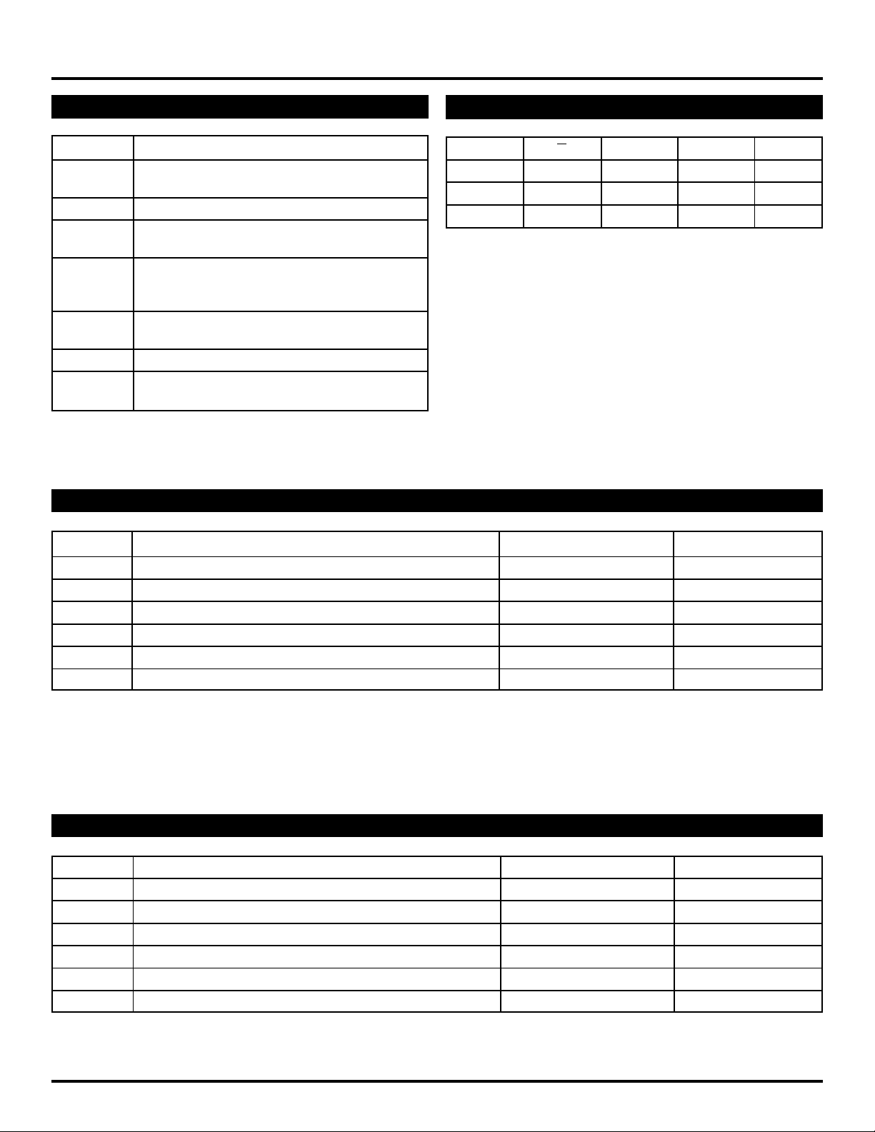
Pin Function
CC Most positive power supply input, +5V for PECL
V
operation.
GND Ground
D
IN, /DIN These differential PECL 100K compatible inputs
receive NRZ data.
/EN This PECL 100K compatible input enables
Laser Driver. Modulation current goes to zero
when asserted HIGH.
OUT, /OUT Open collector outputs from the modulation
buffer drive these differential current outputs.
VREF Voltage reference for use with RSET.
RSET An external resistor sets up the source current
for modulation I
ABSOLUTE MAXIMUM RATINGS
mod.
(1)
D D /EN OUT
LHLHL
HLLLH
XXHHL
NOTES:
1. L = LOW, H = HIGH, X = don't care
2. H = I
OUT = 0mA
(1)
(2)
/OUT
Symbol Rating Value Unit
VCC Power Supply Voltage 0 to +7.0 V
VI Input Voltage 0 to VCC V
IO Output Current 25 mA
TA Operating Temperature Range 0 to +85 °C
Tstore Storage Temperature Range –55 to +125 °C
tot Power Dissipation 250 mW
P
NOTE:
1. Permanent device damage may occur if ABSOLUTE MAXIMUM RATINGS are exceeded. This is a stress rating only and functional operation is not implied
at conditions other than those detailed in the operational sections of this data sheet. Exposure to ABSOLUTE MAXIMUM RATlNG conditions for extended
periods may affect device reliability.
OPERATIONING CONDITIONS
(1)
Symbol Rating Value Unit
VCC Power Supply Voltage +4.5 to +5.5 V
REXT Resistor to Dissipate Power 10 to 50 Ω
RSER Laser Diode Serial Resistor 0 to 50 Ω
RSET Resistor to Adjust Current 1500 to 50,000 Ω
ΘJA Thermal Resistance of Package to Ambient
C
OUT Capacitance on OUT + /OUT 2.5 typical pf
NOTES:
1. The voltage drop across REXT and RSER plus Laser Diode should not be greater than 2V.
2. Still air without heatsink.
(2)
113 °C/W
2
Page 3
Micrel
SY88922
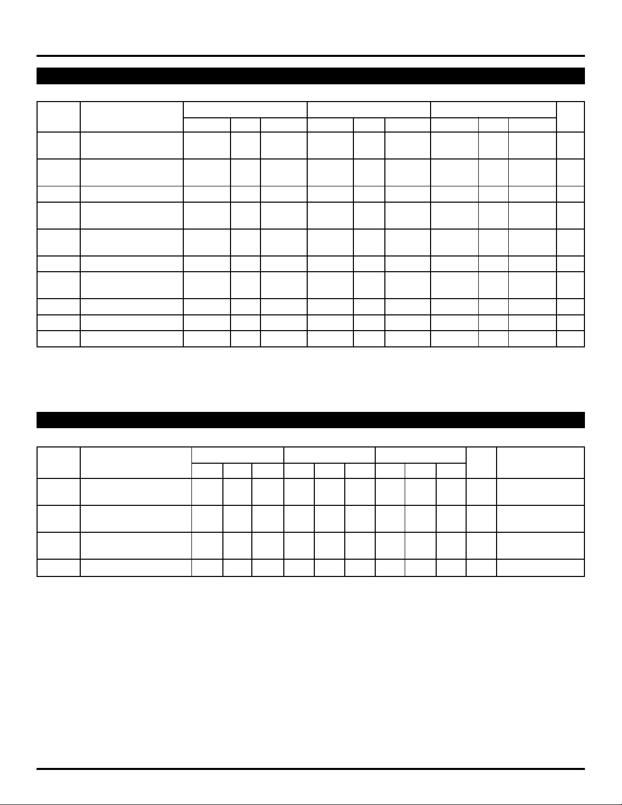
DC ELECTRICAL CHARACTERISTICS
GND = 0V; VCC = +5.0V ±10%; TA = 0°C to + 85°C
TA = 0°CTA = +25°CTA = +85°C
Symbol Parameter Min. Typ. Max. Min. Typ. Max. Min. Typ. Max. Unit
IH Input HIGH Voltage
V
(DIN, /DIN, /EN)
IL Input LOW Voltage
V
(DIN, /DIN, /EN)
VREF Reference Voltage — 3.12 ——3.00 ——2.80 — V
IL Input LOW Current
I
(DIN, /DIN, /EN)
IH Input HIGH Current ——100 ——100 ——100 uA
I
(DIN, /DIN, /EN)
ICC Supply Current
OL Output LOW Current ——500 ——500 ——500 uA
I
(2)
(/EN = HIGH)
IOUT Modulation Current 5 15 25 5 15 25 5 15 25 mA
IRSET Modulation Control 0.125 — 0.625 0.125 — 0.625 0.125 — 0.625 mA
RSET =IOUT/IRSET 30 38 44 30 38 44 30 38 44 —
A
NOTES:
1. VI = VIL(Min.)
2. IMOD = 25mA.
VCC–1165 — VCC–880 VCC–1165 — VCC–880 VCC–1165 — VCC–880
VCC–1810 — VCC–1475 VCC–1810 — VCC–1475 VCC–1810 — VCC–1475
(1)
0.5 —— 0.5 —— 0.5 ——uA
— 16 25 — 16 25 — 16 25 mA
mV
mV
AC ELECTRICAL CHARACTERISTICS
(1)
IMOD =10mA; GND = 0V; VCC = +5V ±10%; TA = 0°C to + 85°C
A = 0°CTA = +25°CTA = +85°C
T
Symbol Parameter Min. Typ. Max. Min. Typ. Max. Min. Typ. Max. Unit Conditions
pd D Propagation Delay ——1000 — 500 1000 ——1000 ps
t
DIN - OUT
pd EN Propagation Delay ——1000 — 450 1000 ——1000 ps
t
/EN - OUT
r Rise/Fall Time ——160 — 110 160 ——160 ps Load = 25Ω
t
tf (20% to 80%)
OR Output Current Ringing
I
NOTES:
1. REXT = RSER = 25Ω ±1%, RSER connects to VCC directly without Laser Diode.
2. IOH = 5 to 25mA
(2)
——10 ——10 ——10 %
3
Page 4
Micrel
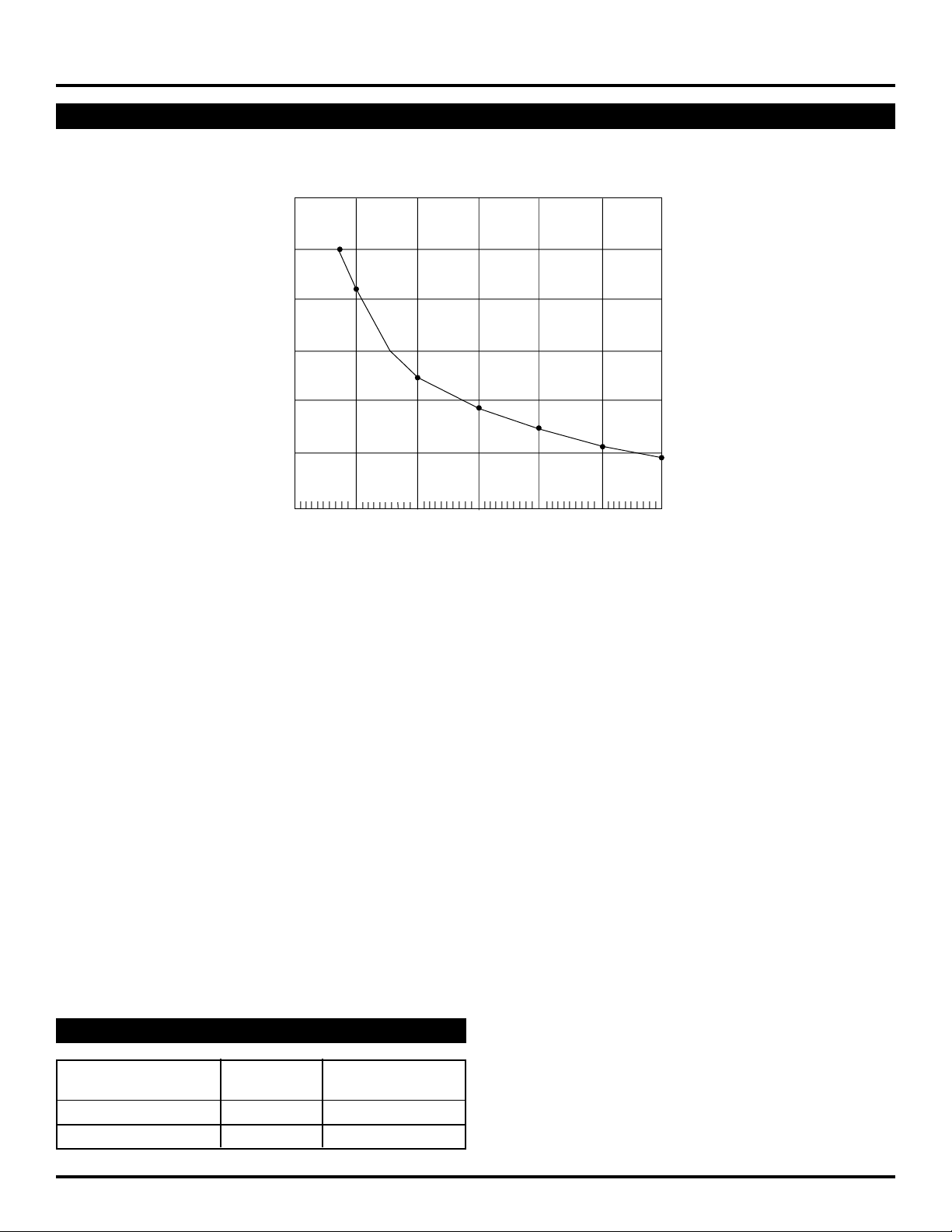
PERFORMANCE CURVES
(mA)
O
I
SY88922
IO and RSET
30
25
20
15
10
5
0.0
0.0
2.0K
4.0K
6.0K
RSET (ohm)
8.0K 10K
12K
PRODUCT ORDERING CODE
Ordering Package Operating
Code Type Range
SY88922KC K10-1 Commercial
SY88922KCTR K10-1 Commercial
4
Page 5
Micrel
D
IN
D
IN
GBIC Terminal
EN
RX_DATA–
RX_DATA+
TX_DATA–
TX_DATA+
RX_LOS
ENABLE/DISABLE
200Ω
V
CC
GND
200Ω
68Ω
68Ω
V
CC
EN
V
CC
GND
V
CC
GND
D
OUT
D
OUT
130Ω
130Ω
82Ω
82Ω
V
CC
OUT
OUT
D
IN
24Ω
V
CC
R
EXT
R
SER
Laserdiode
Photodiode
V
REF
MD
I
BIAS
LOS
OUT
LOS
IN
D
IN
LOS
LVL
I
BIAS SET
SY88905
20kΩ
20kΩ
1000pF
BLM21A102S
Laser
Module
I
BIAS FB
I
PIN SET
LOS
V
REF
SY88923
0.1µF
20kΩ
0.1µF
130Ω
130Ω
82Ω
82Ω
V
CC
20kΩ
SY88922
V
REF
R
SET
The value of RSER
depends on the Laser Diode.
V
CC
V
CC
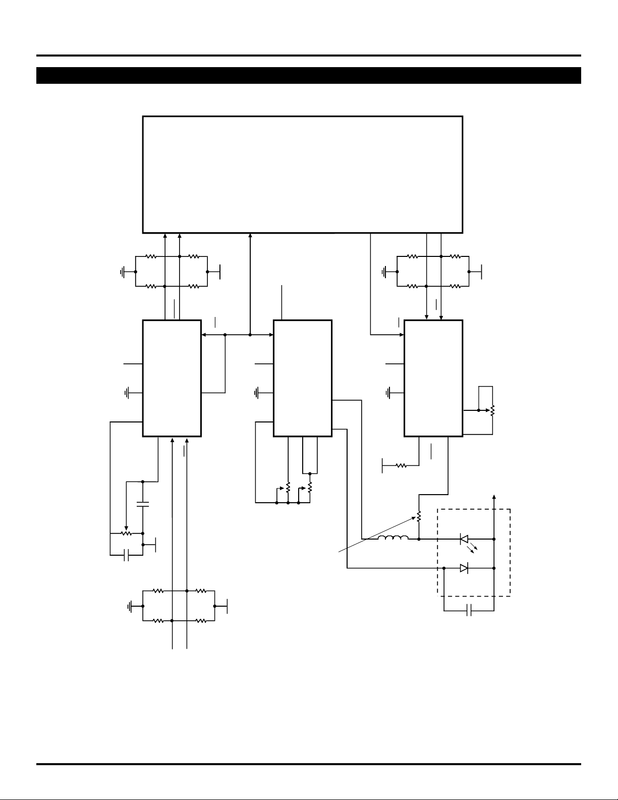
APPLICATION EXAMPLE FOR 3-CHIP SET SOLUTION
SY88922
5
Page 6
Micrel
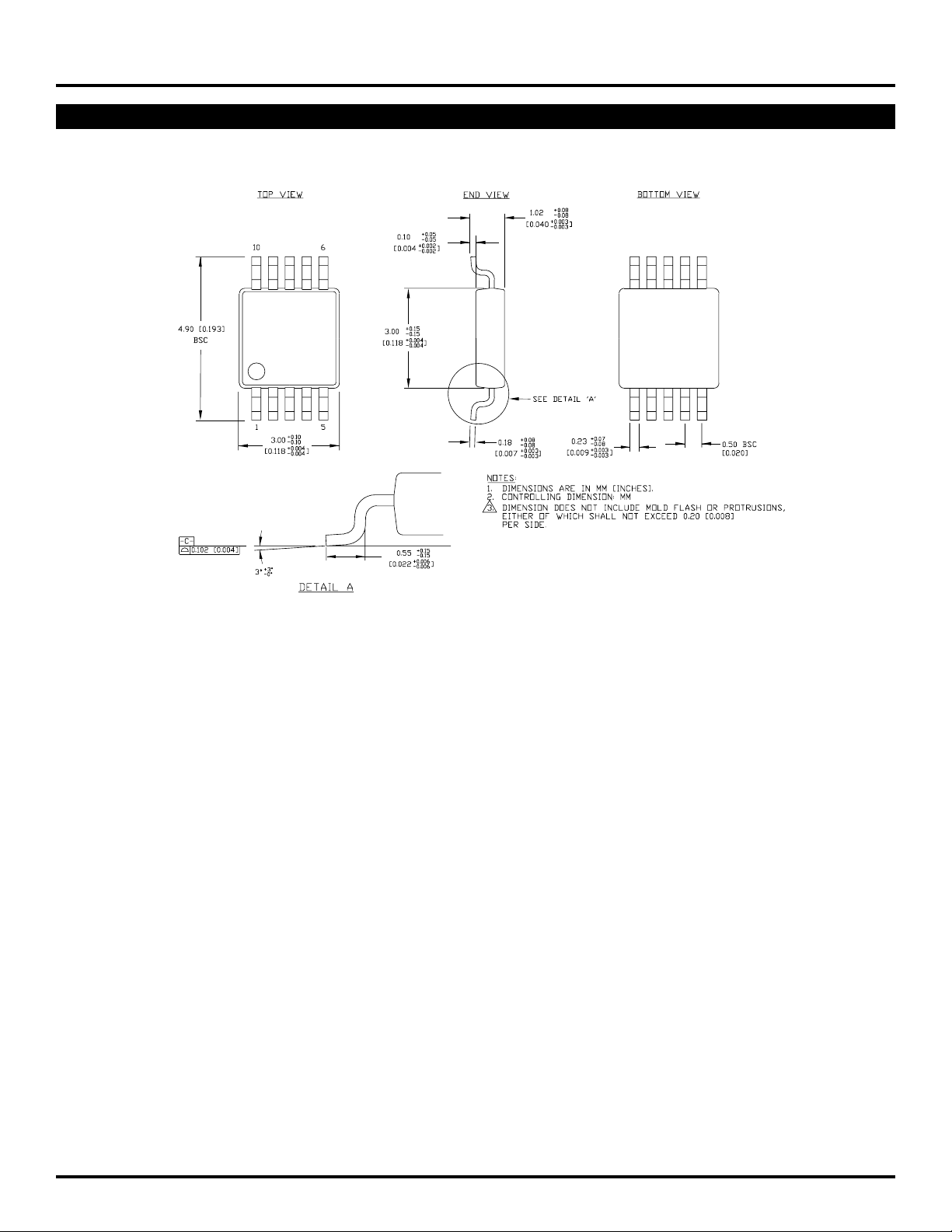
10 LEAD MSOP (K10-1)
SY88922
Rev. 00
6
Page 7

Micrel
SY88922
7
Page 8

Micrel
SY88922
MICREL-SYNERGY 3250 SCOTT BOULEVARD SANTA CLARA CA 95054 USA
TEL + 1 (408) 980-9191 FAX + 1 (408) 914-7878 WEB http://www.micrel.com
This information is believed to be accurate and reliable, however no responsibility is assumed by Micrel for its use nor for any infringement of patents or
other rights of third parties resulting from its use. No license is granted by implication or otherwise under any patent or patent right of Micrel Inc.
© 2000 Micrel Incorporated
8
 Loading...