

Page 1
125MHz WRITE
B
0
2
3
4
5
6
PROGRAMMABLE
TIMING EDGE VERNIER
SY605
FEATURES
■ True 125MHz retrigger rate
■ Pin-compatible with Bt605
■ 15ps delay resolution
■ Less than
± 1 LSB timing accuracy
■ Differential TRIGGER and delay WRITE inputs
■ Delay spans from 4 to 40ns
■ Compatible with 10KH ECL logic
■ Lower power dissipation 350mW typical
■ Available in 28-pin plastic (PLCC) or metal (MLCC)
J-lead package
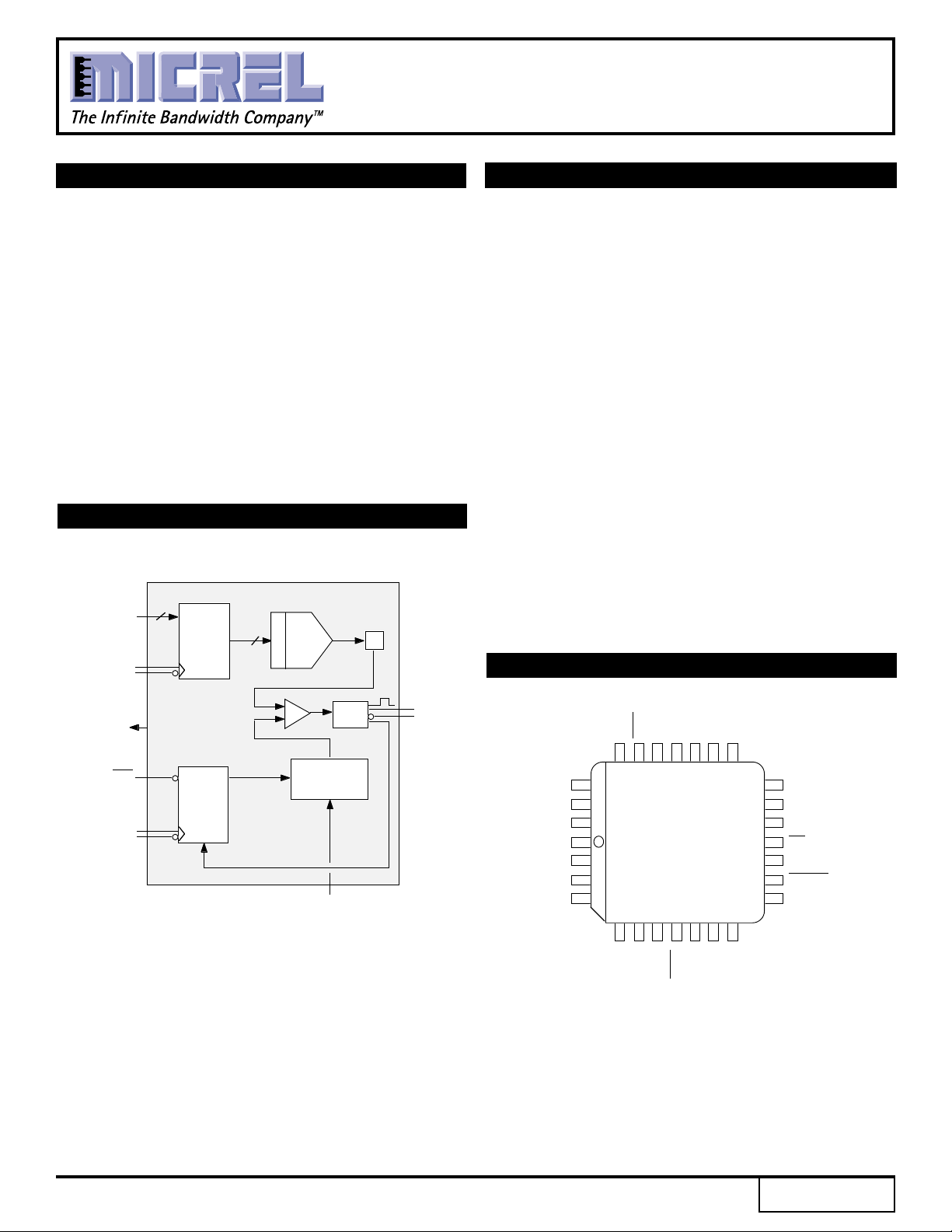
BLOCK DIAGRAM
D0 - D7
WRITE
8
8
LATCH
DAC I/V
DESCRIPTION
Micrel-Synergy's SY605 is an ECL-compatible timing vernier
(delay generator) whose time delay is programmed via an 8bit code which is loaded via an independent "WRITE" input.
The SY605 is fabricated in Micrel-Synergy's proprietary
ASSET™ bipolar process.
This device can be retriggered at speeds up to 125MHz,
with a delay span as short as 4ns. At minimum span, the
resolution is 4ns/255 = 15.7ps per step. The delay span is
externally adjustable up to 40ns. The SY605 employs
differential TRIGGER and WRITE inputs, and produces a
differential OUTPUT pulse; all other control signals are singleended ECL. Edge delay is specified by an 8-bit input which is
loaded into the device with the WRITE signal. The output
pulse width will typically be 3.5ns.
The SY605 is commonly used in Automatic Test Equipment
to provide precise timing edge placement; it is also found in
many instrumentation and communications applications.
Micrel-Synergy's circuit design techniques coupled with
ASSET™ technology result in not only ultra-fast performance,
but allow device operation at lower power dissipation than
competing technologies. Outstanding reliability is achieved in
volume production.
PIN CONFIGURATION
VB
CE
TRIG
+
–
D
FF
0 = STOP
1 = RUN
R
PULSE
GEN
LINEAR
RAMP
GENERATOR
IEXT
OUT
CC
V
25 24 23 21 20 1922
26
D
27
D
1
28
D
1
D
2
D
D
3
4
D
5678910 11
7
D
CC
OUT
OUT
V
TOP VIEW
PLCC
J28-1
EE1
V
TRIG
TRIG
VCCNC
EE0
V
IEXT
NC
18
17
16
15
14
13
12
WRITE
COMP
NC
NC
CE
COMP
WRITE
BB
V
2
1
Rev.: E Amendment: /0
1
Issue Date: May, 1998
Page 2
Micrel
PIN DESCRIPTION
SY605
D0 – D7
Data input pins (ECL compatible). On the falling edge of
WRITE, D0 - D7 are latched into the DAC input register. D0
is the LSB. These inputs specify the amount of delay from the
rising edge of TRIG to the output pulse.
WRITE, WRITE
Differential write inputs (ECL compatible). These inputs
control the parallel data input latch. When WRITE is a logical
one, the data latch is transparent. Data is latched on the falling
edge of WRITE. A single-ended write may be used by
connecting WRITE to V
BB.
CE
Chip enable input (ECL compatible). CE must be a logical
zero on the rising edge of TRIG to enable the device to
respond to the trigger. If CE is floating, the trigger will always
be enabled.
TRIG, TRIG
Differential trigger inputs (ECL compatible). The rising edge
of TRIG is used to trigger the delay cycle if CE is a logical zero.
If CE is a logical one, no operation occurs. It is recommended
that triggering be performed with differential inputs.
OUT, OUT
Differential outputs (ECL compatible).
IEXT
Current reference pin. The amount of current sourced into this
pin determines the span of output delay. The voltage at IEXT
is typically –1.25V.
COMP1, COMP2
Compensation pins. A 0.1µF ceramic capacitor must be
connected between COMP1 and VEE0, and COMP2 and VEE0
(see Figure 3).
VEE
Device power. All VEE pins must be connected.
VCC
Device ground. All VCC pins must be connected together.
VBB
A –1.36V (typical) output.
FUNCTIONAL DESCRIPTION
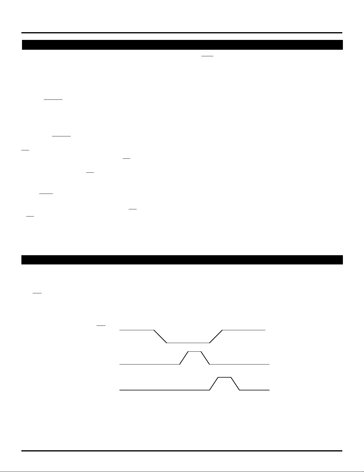
The output pulse generation cycle begins with the arrival of
TRIG shown in Figure 1. The DAC values are latched by the
rising edge of WRITE. Then, when TRIG transitions to a high
and CE is low the linear ramp is initiated.
CE
TRIG
OUT
Figure 1.
When the ramp level reaches that of the DAC, the
comparator initiates the pulse generator to produce an output
pulse resets the ramp and the cycle is ready to begin again.
2
Page 3
Micrel
SY605
ABSOLUTE MAXIMUM RATING
(1)
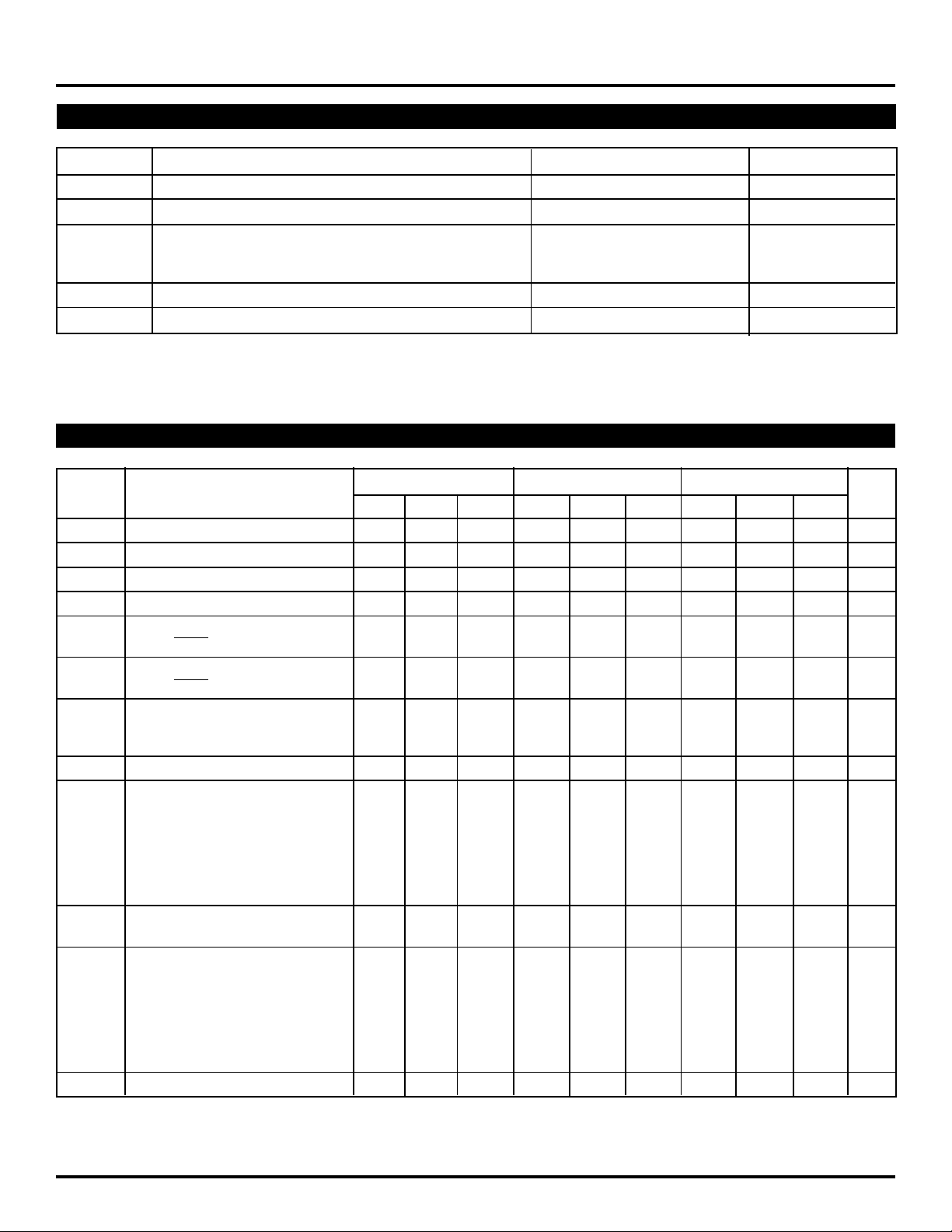
Symbol Parameter Value Unit
VEE Power Supply (VCC = 0V) –8 to 0 V
VI Input Voltage (VCC = 0V) 0 to VEE V
OUT Output Current mA
I
— Continuous 50
— Surge 100
TA Operating Temperature Range 0 to +85 °C
EE Operating Range
V
NOTES:
1. Beyond which device life may be impaired.
2. Parametric values specified at 10E Series: –4.75V to –5.5V
(2)
–5.7 to –4.2 V
DC CHARACTERISTICS
TA = +0˚C TA = +25˚C TA = +70˚C
Symbol Parameter Min. Typ. Max. MIn. Typ. Max. Min. Typ. Max. Unit
VIH Input HIGH Voltage (10K) -1170 — -840 -1130 — -810 -1070 — -735 mV
VIL Input LOW Voltage (10K) -1950 — -1480 -1950 — -1480 -1950 — -1450 mV
VOH Output HIGH Voltage (10K) -1020 -975 -840 -980 -920 -810 -920 -850 -735 mV
VOL Output LOW Voltage (10K) -1950 -1755 -1630 -1950 -1750 -1630 -1950 -1720 -1600 mV
I
IH Input High Current (Vin = VIH max) — 100 150 — 100 150 — 100 150 µA
IIH TRIG, TRIG — 100 150 — 100 150 — 100 150 µA
IL Input Low Current (Vin = VIL min) — 100 150 — 100 150 — 100 150 µA
I
IIL TRIG, TRIG — 100 150 — 100 150 — 100 150 µA
Output Delay Spans
L Differential Linearity Error** — ±0.84 ±0.9 — ±0.84 ±0.9 — ±0.84 ±0.9 LSB
D
IL Integral Linearity Error** — ±1.16 ±1.25 — ±0.89 ±1.0 — ±0.89 ±1.0
VBB VBB Output Voltage -1.44 — -1.25 -1.44 -1.35 -1.25 -1.44 — -1.25 V
EXT IEXT for Tspans
I
Tspan = 4ns 1.80 2.38 2.80 1.80 2.38 2.80 1.80 2.38 2.80 mA
Tspan = 5ns 1.45 1.85 2.40 1.45 1.85 2.40 1.45 1.85 2.40 mA
Tspan = 10ns 0.70 0.93 1.20 0.70 0.93 1.20 0.70 0.93 1.20 mA
Tspan = 15ns 0.45 0.62 0.80 0.45 0.62 0.80 0.45 0.62 0.80 mA
Tspan = 20ns 0.34 0.46 0.60 0.34 0.46 0.60 0.34 0.46 0.60 mA
Tspan = 30ns 0.20 0.30 0.40 0.20 0.30 0.40 0.20 0.30 0.40 mA
Tspan with I
(Tspan = Tmax - Tmin) 4.1 — 6.5 4.1 — 6.5 4.1 — 6.5 ns
Tmin Minimum Delay Time*
Data = 00, Tspan = 5ns — 2.8 3.8 — 2.8 3.8 — 2.8 3.8 ns
EE VEE Supply Current ——100 — 70 100 ——100 mA
I
NOTE:
1. 10K series circuits are designed to meet the DC specifications shown in the table after thermal equilibrium has been established. The circuit is in a test
socket or mounted on a printed circuit board and transverse air flow greater than 500 lfpm is maintained. Outputs are terminated through a 50Ω resistor
to -2.0 volts.
EXT = 1.8 mA
Tspan = 10ns — 3.4 4.9 — 3.4 4.9 — 3.4 4.9 ns
Tspan = 15ns — 4.0 6.0 — 4.0 6.0 — 4.0 6.0 ns
Tspan = 20ns — 4.6 7.1 — 4.6 7.1 — 4.6 7.1 ns
Tspan = 25ns — 5.2 8.2 — 5.2 8.2 — 5.2 8.2 ns
Tspan = 30ns — 5.8 9.3 — 5.8 9.3 — 5.8 9.3 ns
3
Page 4
Micrel
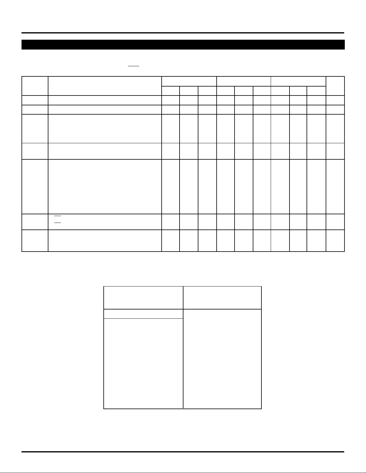
AC CHARACTERISTICS
SY605
ECL input values are -0.9 to -1.7V, with input rise/fall times ≤ 2ns,
measured between the 20% and 80% points. Timing reference
points at 50% for inputs and outputs. OUT and OUT loading with 50Ω
Symbol Parameter Min. Typ. Max. Min. Typ. Max. Min. Typ. Max. Unit
fMAX Trigger Rate
tWI Trigger Width High 2.0 1.0 — 2.0 1.0 — 2.0 1.0 — ns
t
WO Output Pulse Width High Time 2.5 3.5 4.5 2.5 3.5 4.5 2.5 3.5 4.5 ns
Output Pulse Rise/Fall Time (20/80%) — 550 750 — 550 750 — 550 750 ps
t
S Output Pulse Spacing
Minimum Delay Time vs. Tspan
(1)
Span = 4ns @ 1 LSB 8.0 ——8.0 ——8.0 ——ns
——125 ——125 ——125 MHz
to -2.0V. Typical values are based on nominal temperature, i.e., and
nominal voltage, i.e., - 5.2V.
TA = +0°CTA = +25°CTA = +70°C
∆ T00 / ns (Tspan = 5 to 10ns) — 125 220 — 125 220 — 125 220 ps/ns
Output Delay ns
1 LSB Tspan (Tspan = Tmax - Tmin) 4.0 — 40 4.0 — 40 4.0 — 40 ns
1 LSB Resolution (Tspan / 225) 15.7 — 157 15.7 — 157 15.7 — 157 ps
Tempo (5ns Span)
∆ Tspan /°C — 2 —— 2 —— 2 — ps/°C
∆ Tmin /°C — 2 —— 2 —— 2 — ps/°C
Power Supply Rejection — 60 ——60 ——60 — ps/V
(Data = 0-FF HEX, Tspan = 5ns)
S CE Setup Time 2.0 ——2.0 ——2.0 ——ns
t
tH CE Hold Time 1.5 ——1.5 ——1.5 ——ns
t
WH WRITE Pulse Width High Time 2.0 ——2.0 ——2.0 ——ns
tDS D0 - D7 Setup Time 1.0 ——1.0 ——1.0 ——ns
tDH D0 - D7 Hold Time 1.5 ——1.5 ——1.5 ——ns
NOTE:
1. See chart below:
Maximum Tspan and Trigger Rates
Maximum Tspan (ns) Minimum Trigger
Maintaining Linearity Periods (ns)
of ±1 LSB
4.0 8.0
5.1 10.0
5.8 11.1
6.75 12.5
8.1 14.3
9.9 16.6
12.0 20.0
15.5 25.0
22.0 33.3
The information in this table is guaranteed but not 100% production tested.
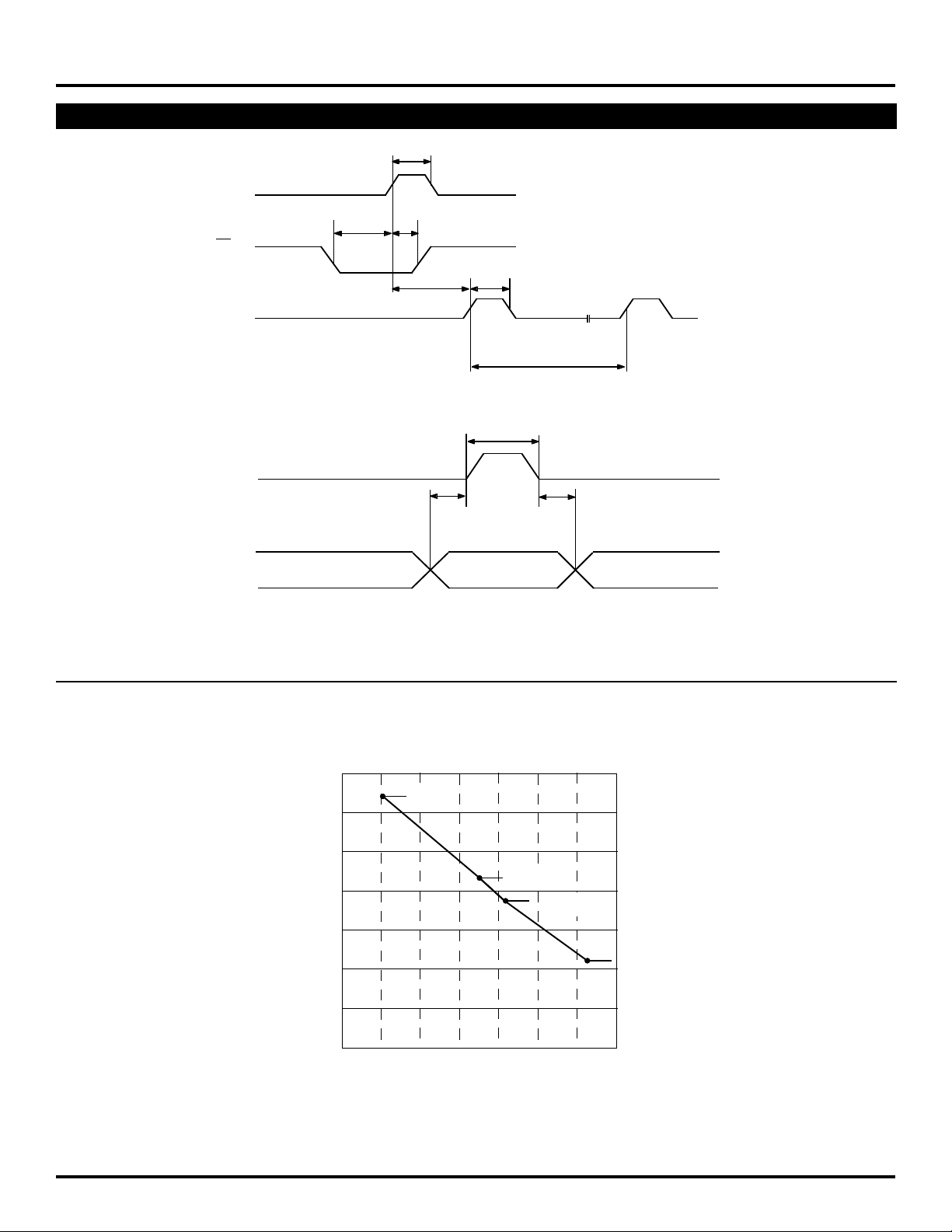
See Figure 2 for a graphical representation.
4
Page 5
Micrel
TIMING DIAGRAMS
TRIG
CE
SY605
t
WI
t
SU
t
H
OUT
WRITE
D0 -D7
DELAY
t
DSU
t
WO
t
DATA
S
t
WH
t
DH
±±±± 1 LSB
Span vs. Trigger Rates
9
8
7
6
5
Span (ns)
4
3
2
60 70 80 90 100 110 120 130
INL
- 0.92LSB
INL
- 0.86LSB
Frequency (MHz)
Figure 2.
INL
- 0.9LSB
INL
- 1.14LSB
5
Page 6
Micrel
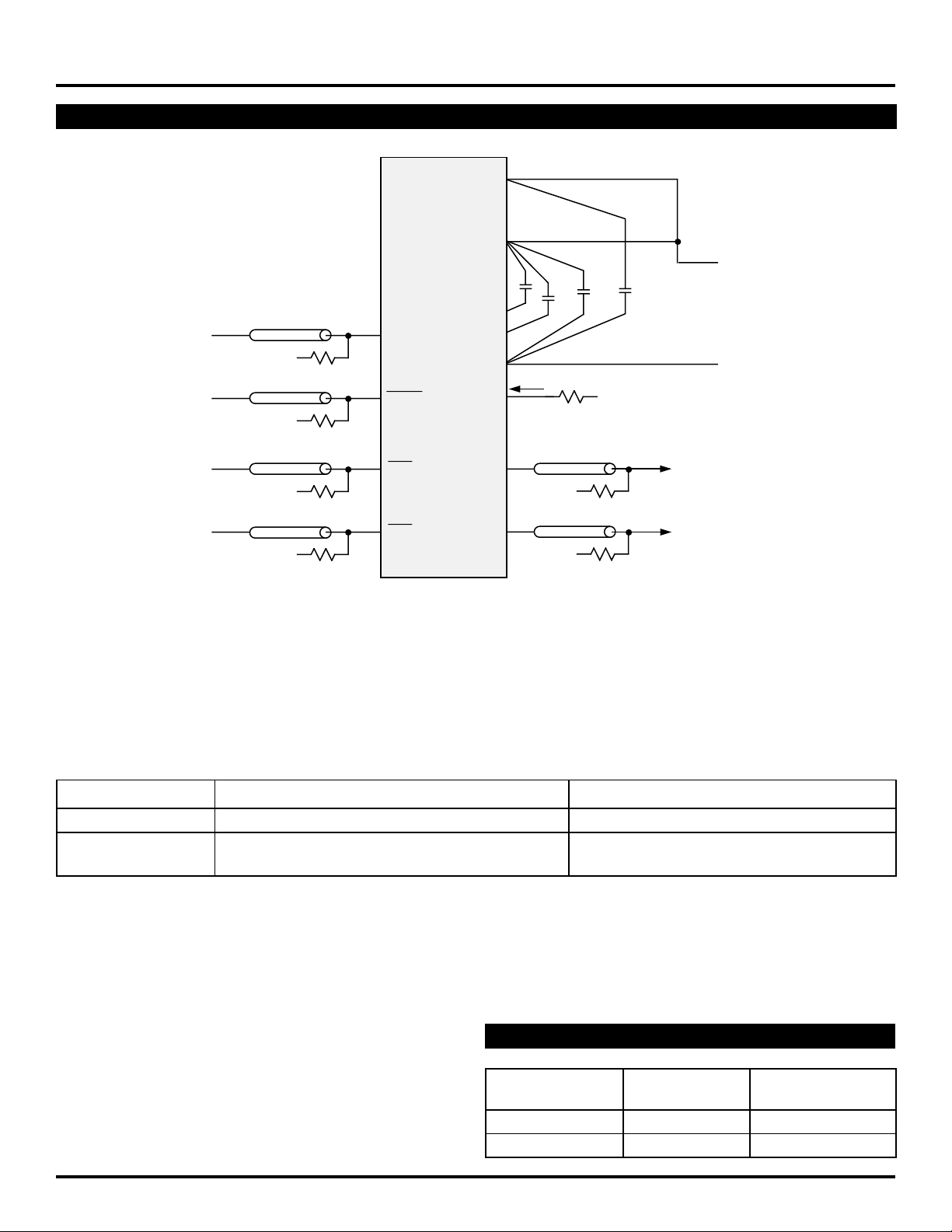
APPLICATION DIAGRAM
ZO = 50Ω
ZO = 50
ZO = 50Ω
ZO = 50Ω
REXT Calculation:
–2.0V
–2.0V
–2.0V
–2.0V
50Ω
50Ω
50Ω
50Ω
WRITE
WRITE
TRIG
TRIG
SY605
V
EE1
V
EE0
COMP1
COMP2
CC
V
IEXT
OUT
OUT*
C3
ZO = 50Ω
ZO = 50Ω
SY605
–5.2V
C4
REXT
I
–2.0V
50Ω
–2.0V
C2
50Ω
C1
GROUND
VEXT
REXT = (VEXT + 1.25V)/IEXT
For Example:
If Tspan is around 15ns, then IEXT is around 0.6mA, (see DC Characteristic Table) and assume IEXT pin is tied
to VCC with the resistor.
REXT
= 0 + 1.25V/0.6mA
= 2.08K ohm
Location Description Vendor Part Number
C1–C4 0.1µF ceramic capacitor Erie RPE112Z5U104M50V
REXT 1% metal film resistor CB301210
(selected for proper Tspan) Dale CMF-55C
NOTE:
The vendor numbers above are listed only as a guide. Substitution of devices with similar characteristics will not affect the performance of the SY605.
All devices should be as close as possible to the SY605.
Figure 3. Typical Connection Diagram and Parts List.
PRODUCT ORDERING CODE
Ordering Package Operating
Code Type Range
SY605JC J28-1 Commercial
SY605JCTR J28-1 Commercial
6
Page 7
Micrel
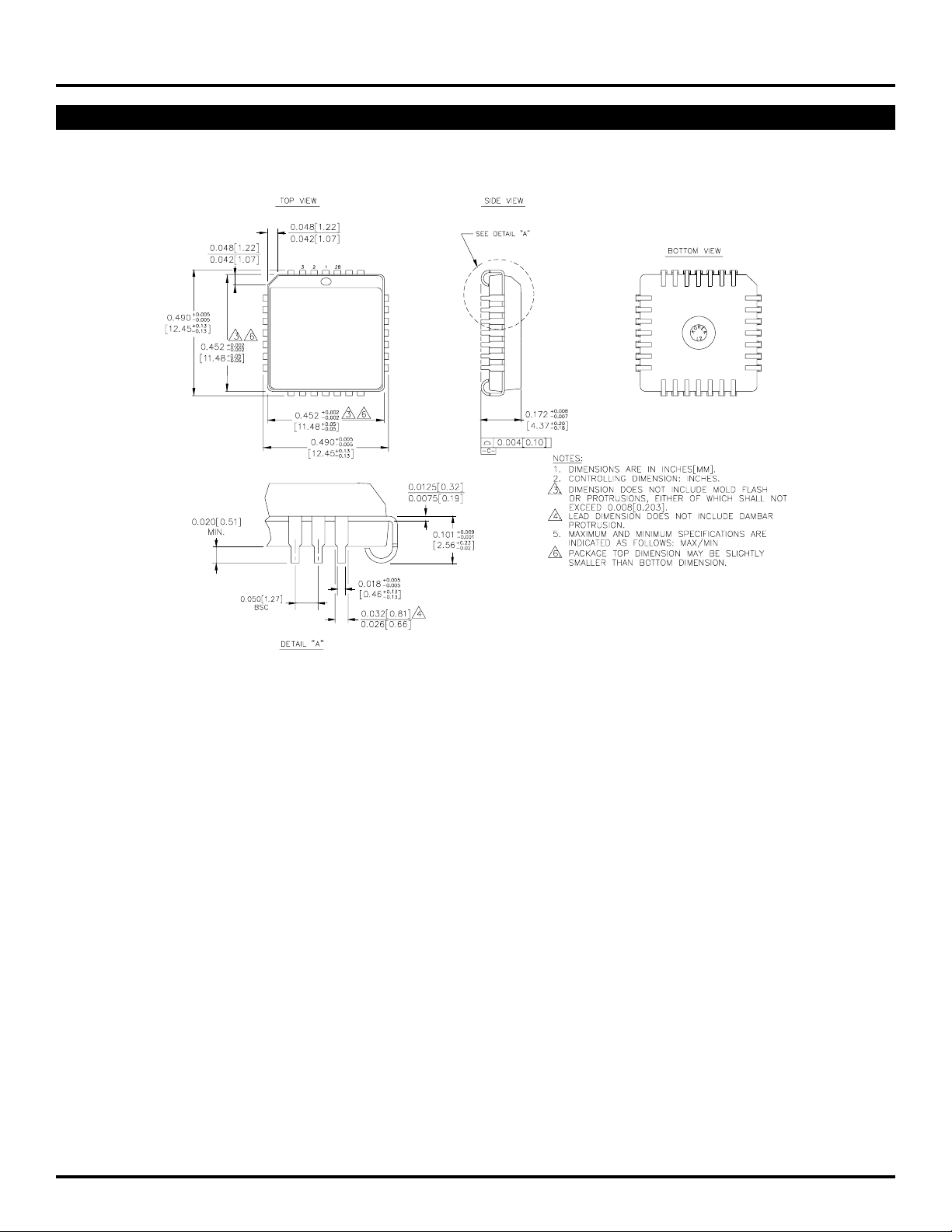
28 LEAD PLCC (J28-1)
SY605
Rev. 03
7
Page 8

Micrel
SY605
MICREL-SYNERGY 3250 SCOTT BOULEVARD SANTA CLARA CA 95054 USA
TEL + 1 (408) 980-9191 FAX + 1 (408) 914-7878 WEB http://www.micrel.com
This information is believed to be accurate and reliable, however no responsibility is assumed by Micrel for its use nor for any infringement of patents or
other rights of third parties resulting from its use. No license is granted by implication or otherwise under any patent or patent right of Micrel Inc.
© 2000 Micrel Incorporated
8
 Loading...