

Page 1
Micrel, Inc.
2.5V/3.3V 3.0GHZ DUAL 2 x 2 CML
CROSSPOINT SWITCH
W/INTERNAL TERMINATION
FEATURES
■ Guaranteed AC parameters over temperature:
•f
•tr/ tf < 120ps
• Within-device skew < 25ps
■ Non-blocking “switch architecture”
■ Configurable as dual 2:1 mux, dual 1:2 fanout buffer,
1:4 fanout buffer, quad buffer, or dual 2 x 2 switch
■ 50Ω compatible outputs
■ Unique input termination and VT pin for DC-coupled
and AC-coupled input signals–CML or PECL
■ Fully differential inputs/outputs
■ TTL/CMOS compatible control logic
■ Wide supply voltage range: 2.3V to 3.6V
■ Wide operating temperature range: –40°C to +85°C
■ Available in 32-pin EPAD-TQFP package
> 3.0GHz (3Gbps)
MAX
SuperLite™
SuperLite™
SY55858U
SY55858U
SuperLite™
DESCRIPTION
The SY55858U is a low-voltage, high-speed dual 2 x 2
crosspoint switch with a flexible input that accepts CML
or PECL, and a 50Ω compatible differential CML (currentmode logic) output. The non-blocking design allows any
input to connect to any output. Varying the state of the
select inputs allows SY55858U to be used in backup,
fault tolerant, protection and backplane distribution
applications.
The signal inputs (DA
internal termination design that allows access to the
termination network through VT pins. This feature allows
the device to easily interface to other logic standards
such as AC-coupled or DC-coupled PECL/LVPECL
signals. For applications that require a single-channel
2 x 2 crosspoint, consider the SY55854.
and DB
0–1
) have a unique
0–1
APPLICATIONS
■ SONET/SDH optical transport
■ Backplane redundancy
■ Add-drop Multiplexers
SuperLite is a trademark of Micrel, Inc.
M9999-110705
[email protected] or (408) 955-1690
1
Rev.: D Amendment: /0
Issue Date: November 2005
Page 2
Micrel, Inc.
/
/
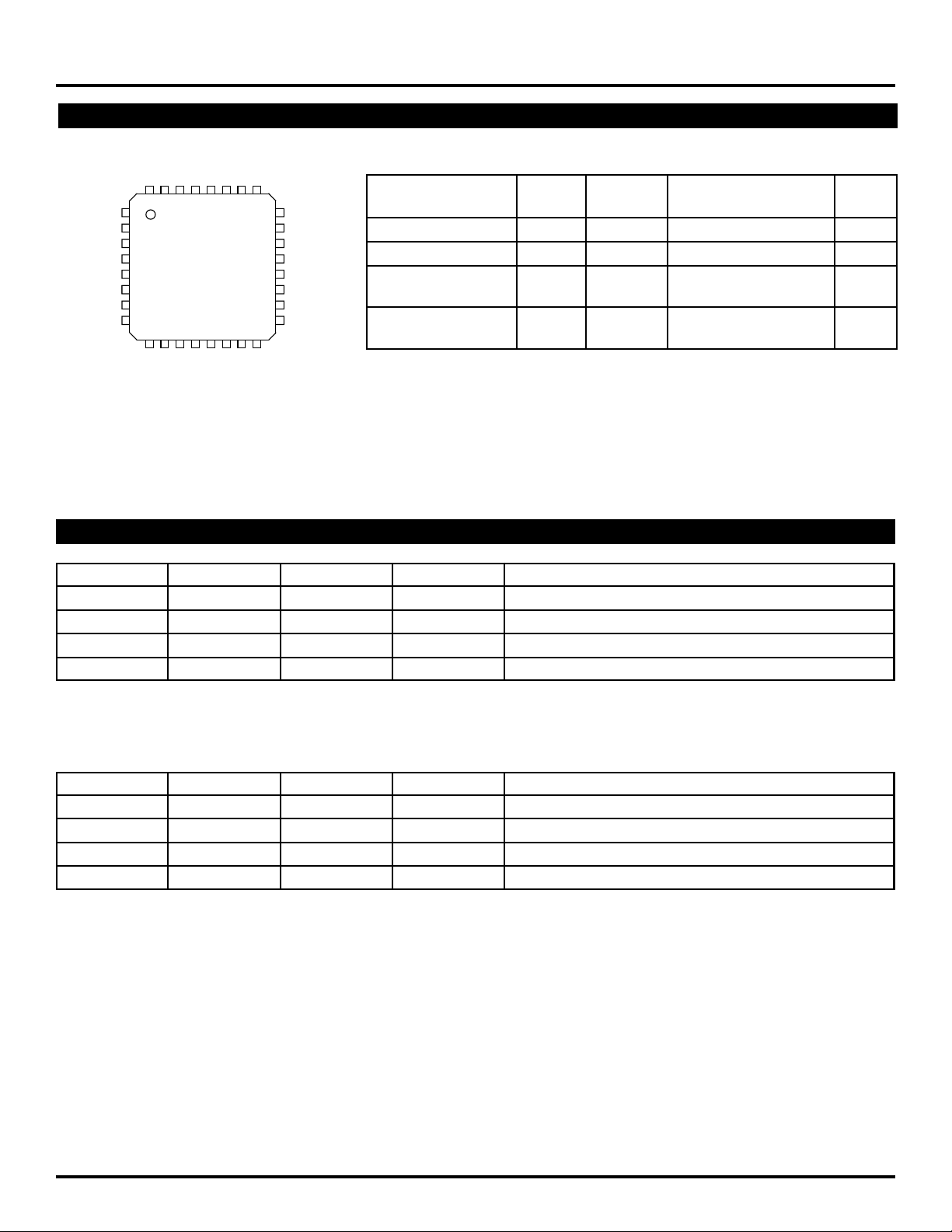
PACKAGE/ORDERING INFORMATION
SuperLite™
SY55858U
(1)
Package Operating Package Lead
H32-1 Industrial SY55858UHI Sn-Pb
H32-1 Industrial SY55858UHG with Pb-Free
Pb-Free bar-line indicator NiPdAu
H32-1 Industrial SY55858UHG with Pb-Free
Pb-Free bar-line indicator NiPdAu
VTA1
/DA1
SELA0
DA1
SELA1
/DA0
VTA0
32 31 30 29 28 27 26 25
DB1
1
VTB1
2
3
/DB1
SELB0
DB0
VTB0
/DB0
SELB1
Top View
4
EPAD-TQFP
5
6
7
8
H32-1
910111213141516
GND
VCC
QB0
QB0
VCC
QB1
QB1
32-Pin EPAD-TQFP (H321)
DA0
24
23
22
21
20
19
18
17
VCC
GND
VCC
QA0
/QA0
VCC
QA1
/QA1
VCC
Ordering Information
Part Number Type Range Marking Finish
SY55858UHI H32-1 Industrial SY55858UHI Sn-Pb
SY55858UHITR
SY55858UHG
SY55858UHGTR
Notes:
1. Contact factory for die availability. Dice are guaranteed at TA = 25°C, DC Electricals only.
2. Tape and Reel.
(2)
(3)
(2, 3)
3. Pb-Free package recommended for new designs.
TRUTH TABLES
SELA0 SELA1 QA0 QA1 Function
0 0 DA0 DA0 Fanout Buffer or Redundant Distribution
0 1 DA0 DA1 Dual Buffer or Crosspoint
1 0 DA1 DA0 Dual Buffer or Crosspoint
1 1 DA1 DA1 Fanout Buffer or Redundant Distribution
Table 1. Input to Output Connectivity Crosspoint A
SELB0 SELB1 QB0 QB1 Function
0 0 DB0 DB0 Fanout Buffer or Redundant Distribution
0 1 DB0 DB1 Dual Buffer or Crosspoint
1 0 DB1 DB0 Dual Buffer or Crosspoint
1 1 DB1 DB1 Fanout Buffer or Redundant Distribution
Table 2. Input to Output Connectivity Crosspoint B
M9999-110705
[email protected] or (408) 955-1690
2
Page 3
SuperLite™
Micrel, Inc.
PIN DESCRIPTION
Pin Number Pin Name Pin Function
1 DB1 Channel B1 posititve signal input.
2 VTB1 Channel B1 termination center-tap. For CML inputs, leave this pin floating.
Otherwise, see Figures 5a–5d in “Input Interface Application” section.
3 /DB1 Channel B1 negative signal input.
4 SELB0 Channel B0 output select. TTL/CMOS input.
5 DB0 Channel B0 positive signal input.
6 VTB0 Channel B0 termination center-tap. For CML inputs, leave this pin floating.
Otherwise, see Figures 5a–5d in “Input Interface Application” section.
7 /DB0 Channel B0 negative signal input.
8 SELB1 Channel B1 output select. TTL/CMOS input.
9, 24 GND Supply Ground.
10, 13, 16, 17, 20, 23 VCC Positive supply normally connect to 2.5V, 3.3V, or 5V nominal supply, and
bypass each pin with 0.1µF//0.01µF low ESR capacitors.
11 /QB0 Channel B0 negative signal output. 50Ω CML.
12 QB0 Channel B0 positive signal output. 50Ω CML.
14 /QB1 Channel B1 negative signal output. 50Ω CML.
15 QB1 Channel B1 positive signal output. 50Ω CML.
18 /QA1 Channel A1 negative signal output. 50Ω CML.
19 QA1 Channel A1 positive signal output. 50Ω CML.
21 /QA0 Channel A0 negative signal output. 50Ω CML.
22 QA0 Channel A0 positive signal output. 50Ω CML.
25 DA0 Channel A0 positive signal input.
26 VTA0 Channel A0 termination center-tap. For CML inputs, leave this pin floating.
Otherwise, see Figures 5a–5d in “Input Interface Application” section.
27 /DA0 Channel A0 negative signal input.
28 SELA1 Channel A1 output select. TTL/CMOS input.
29 DA1 Channel A1 positive signal input.
30 VTA1 Channel A1 termination center-tap. For CML inputs, leave this pin floating.
Otherwise, see Figures 5a–5d in “Input Interface Application” section.
31 /DA1 Channel A1 negative signal input.
32 SELA0 Channel A1 output select. TTL/CMOS input.
SY55858U
M9999-110705
[email protected] or (408) 955-1690
3
Page 4
Micrel, Inc.
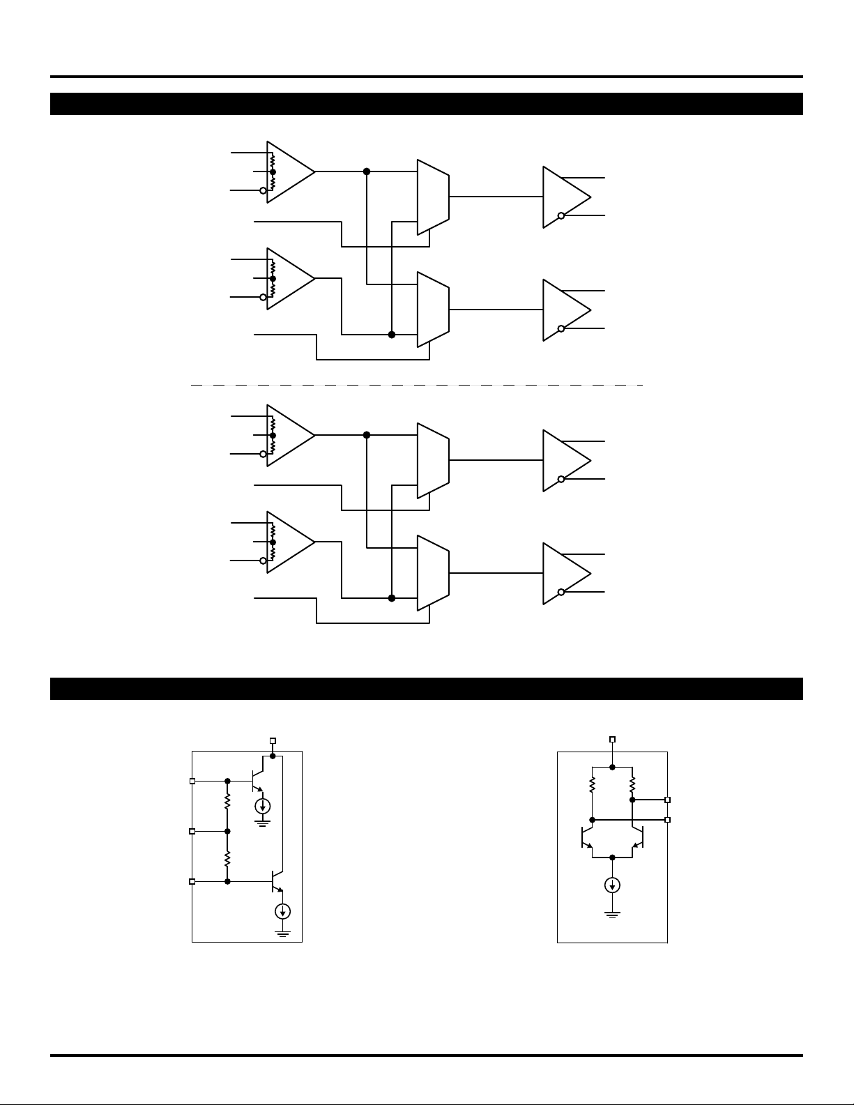
FUNCTIONAL BLOCK DIAGRAM
SuperLite™
SY55858U
DA0
/DA0
SELA0
DA1
/DA1
SELA1
DB0
/DB0
SELB0
DB1
/DB1
SELB1
TA0
TA1
50Ω
50Ω
50Ω
50Ω
50Ω
50Ω
50Ω
50Ω
0
A0
CML
1
0
A1
CML
1
0
B0
CML
1
0
B1
CML
1
QA0
/QA0
QA1
/QA1
QB0
/QB0
QB1
/QB1
V
V
V
TB0
V
TB1
INPUT AND OUTPUT STAGE
V
CC
D0
50Ω
*
V
T
/D0
Figure 1. Input Stage
Note 1. See “Input Interface Applications” section for proper input
M9999-110705
[email protected] or (408) 955-1690
connection.
1.2mA
50Ω
1.2mA
SY55858U
v
cc
50Ω 50Ω
16mA
SY55858U
Q
/Q
Figure 2. Output Stage
4
Page 5
Micrel
SuperLite™
SY55858U
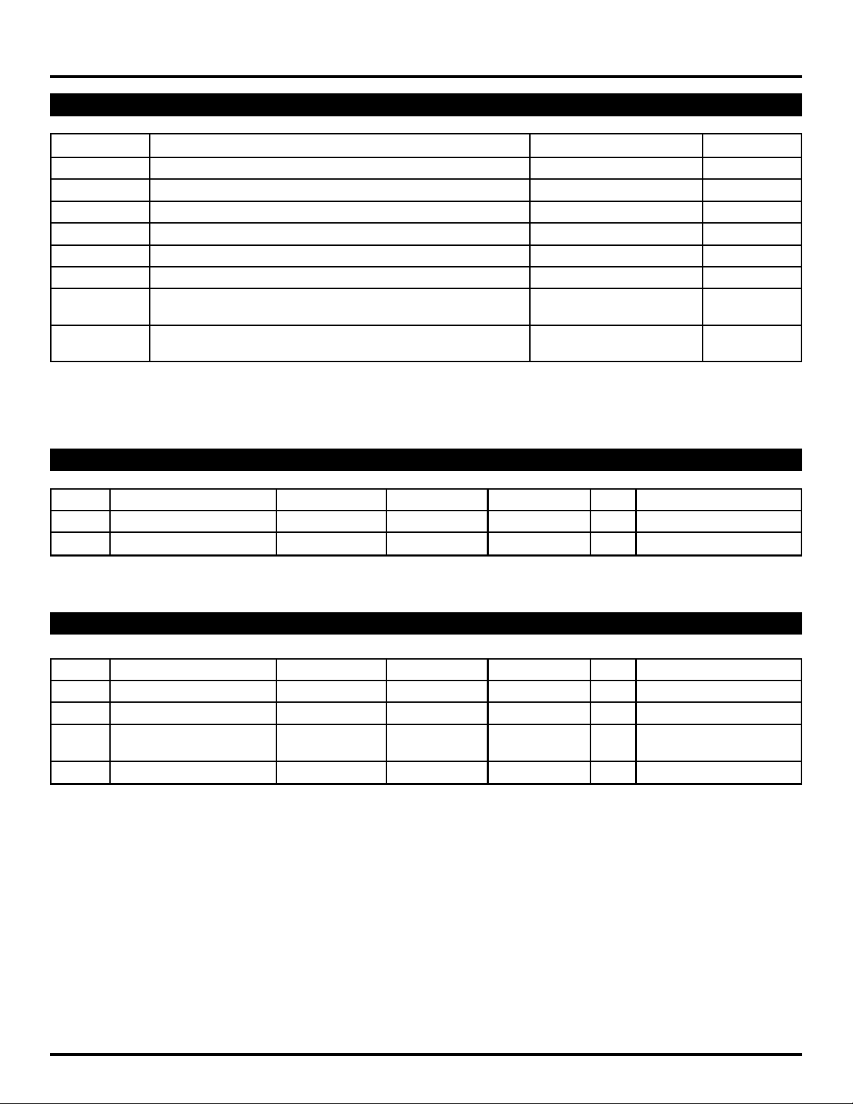
ABSOLUTE MAXIMUM RATINGS
(1)
Symbol Rating Value Unit
V
V
V
T
T
T
θ
CC
IN
OUT
A
LEAD
store
JA
Power Supply Voltage –0.5 to +6.0 V
Input Voltage –0.5 to V
+0.5 V
CC
CML Output Voltage VCC –1.0 to VCC +0.5 V
Operating Temperature Range –40 to +85 °C
Lead Temperature (soldering, 20sec.) 260 °C
Storage Temperature Range –65 to +150 °C
Package Thermal Resistance –Still-Air (multi-layer PCB) 28 °C/W
(Junction-to-Ambient) –500lfpm (multi-layer PCB) 20 °C/W
θ
JC
Package Thermal Resistance 4 °C/W
(Junction-to-Case)
Note 1. Permanent device damage may occur if absolute maximum ratings are exceeded. This is a stress rating only and functional operation is not
implied at conditions other than those detailed in the operational sections of this data sheet. Exposure to absolute maximum ratlng conditions
for extended periods may affect device reliability.
DC ELECTRICAL CHARACTERISTICS
Symbol Parameter Min. Typ. Max. Unit Condition
V
CC
I
CC
Power Supply Voltage 2.3 — 3.6 V
Power Supply Current — 150 190 mA No load, over temp.
TTL CONTROL ELECTRICAL CHARACTERISTICS
VCC = 2.3V to 3.6V; GND = 0V; TA = –40°C to +85°C
Symbol Parameter Min. Typ. Max. Unit Condition
V
IH
V
IL
I
IH
I
IL
Note 2. Specifications are guaranteed after thermal equilibrium has been establised.
Input HIGH Voltage 2.0 ——V
Input LOW Voltage ——0.8 V
Input HIGH Current ——+20 µAVIN = 2.7V, VCC = Max.
——+100 µAVIN = VCC, VCC = Max.
Input LOW Current –300 ——µAVIN = 0.5V, VCC = Max.
(2)
5
Page 6
SuperLite™
Micrel, Inc.
SY55858U
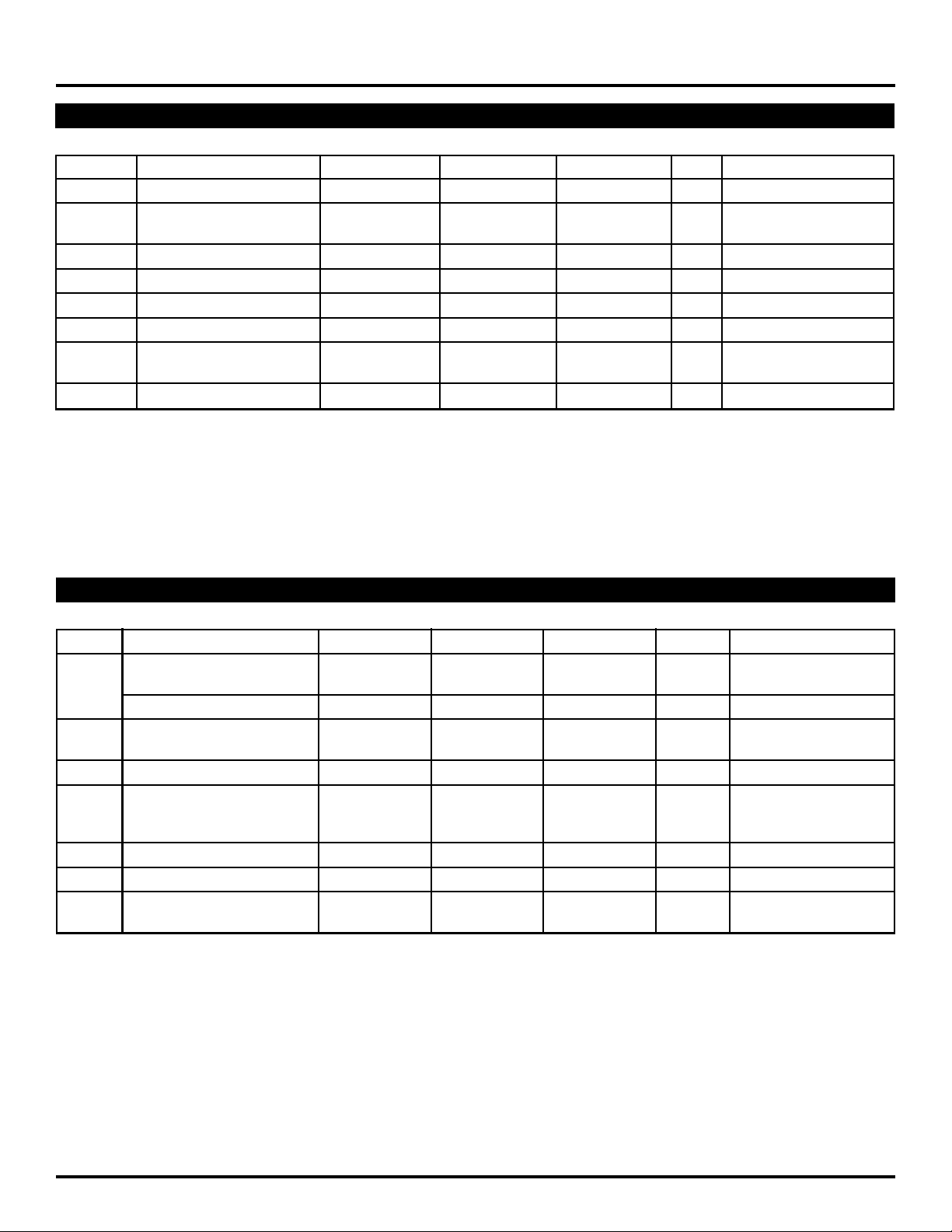
CML DC ELECTRICAL CHARACTERISTICS
VCC = 2.3V to 3.6V; GND = 0V; TA = –40°C to +85°C
Symbol Parameter Min. Typ. Max. Unit Condition
V
ID
R
IN
V
IH
V
IL
V
OH
V
OL
V
OUT(SWING)
R
OUT
Note 3. Device is guaranteed to meet the DC specifications, shown in the table above, after thermal equilibrium has been established. The device is
Note 4. V
Differential Input Voltage 100 ——mV
Differential Input Resistance
D-to-/D 90 100 110 Ω
Input HIGH Voltage 1.6 — V
Input LOW Voltage 1.5 — VCC – 0.1 V
Output HIGH Voltage VCC – 0.040 VCC – 0.010 V
Output LOW Voltage VCC – 1.00 VCC – 0.800 VCC – 0.650 V No Load
Output Voltage Swing
(4)
0.650 0.800 1.00 V No Load
Output Source Impedance 40 50 60 Ω
tested in a socket such that traverse airflow ≥500lfpm is maintained.
OUT(SWING)
purposes is 2 ×V
swing is available in the 50Ω environment. Refer to the “CML Output Termination Application” section, Figures 3 and 4, for more details.
is defined as the swing on one output of a differential pair, that is |VOH – VOL| on one pin. The swing for common mode immunity
OUT(SWING)
. Actual voltage levels and differential swing will depend on customer termination scheme. Typically, a 400mV
(3)
CC
CC
V
V No Load
— 0.400 — 50Ω Environment
AC ELECTRICAL CHARACTERISTICS
VCC = 2.3V to 3.6V; GND = 0V; TA = –40°C to +85°C
Symbol Parameter Min. Typ. Max. Unit Condition
f
MAX
t
PLH
t
PHL
t
SWITCH
t
SKEW
R
J
D
J
tr, t
f
Note 5. Tested using environment of Figure 3, 50Ω equivalent load. AC parameters are guaranteed by design and characterization.
Note 6. f
Note 7. Input TTL/CMOS edge rate of <1.5ns.
Note 8. Worst-case difference between QA0 and QA1 from either DA0 or DA1 (or between QB0 and QB1 from either DB0 or DB1 respectively), when
Note 9. Worst-case difference between QA and QB outputs, when DA or DB inputs are shorted.
Maximum Frequency
NRZ Data Rate 3.0 ——Gbps
Clock Frequency
(6)
3.0 ——GHz
Differential Propagation Delay 220 350 450 ps
D-to-Q
(8)
(9)
(7)
— 0.50 1.0 ns
— 12 25 ps
— 25 50 ps
Select-to-Valid Output
Within-Device Skew
Within-Device Skew
Part-to-Part Skew (Diff.) — 100 —
Random Jitter — 25ps
Deterministic Jitter — 520ps
CML Output Rise/Fall Times — 80 120 ps
(20% to 80%)
clock is defined as the maximum toggle rate the device can operate while still achieving a 250mV minimum CML output swing, 50Ω
MAX
equivalent load.
both outputs come from the same input.
(5)
RMS
PP
M9999-110705
[email protected] or (408) 955-1690
6
Page 7
Micrel, Inc.
T
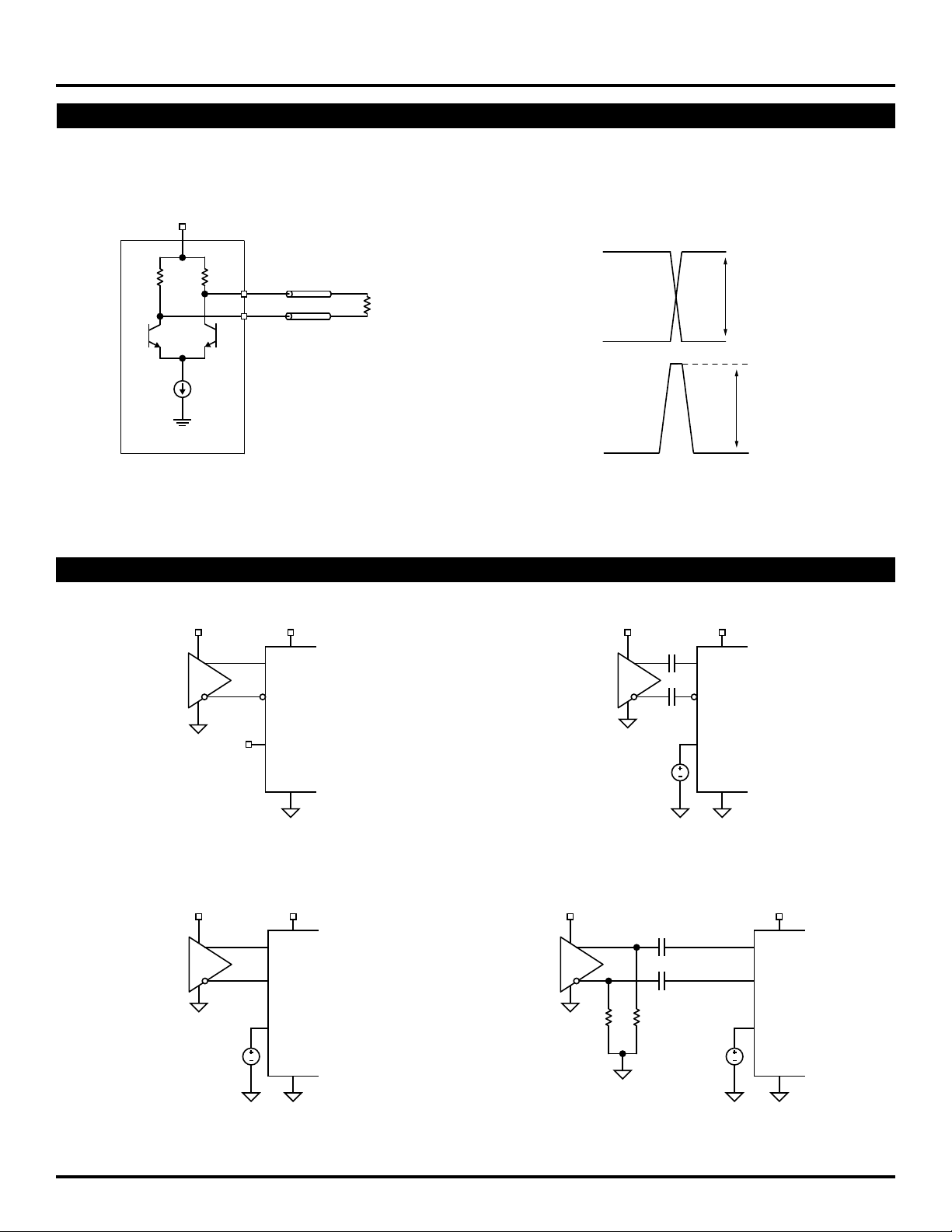
CML OUTPUT TERMINATION APPLICATION
SuperLite™
SY55858U
All CML inputs accept a CML output from any other
member of this family. All CML outputs are source terminated
v
cc
50Ω 50Ω
16mA
SY55858U
50Ω
100Ω
50Ω
Figure 3. 50Ω Output Termination
INPUT INTERFACE APPLICATIONS
50Ω differential drivers as shown in Figure 3.
+
Q
OUT
400mV
(Single-Ended)
/Q
OUT
Q
OUT
800mV
(Q
OUT — /QOU
Differential
/Q
OUT
Figure 4. Output Levels
V
CC
CML
V
D
/D
VTNC
CC
SY55858
Figure 5a. CML-to-CML
(DC-Coupled) Input Interface
V
CC
PECL
VCC – 2.0V
V
D
/D
SY55858
VT
CC
V
CC
CML
VCC – 1.3V
V
D
/D
SY55858
VT
CC
Figure 5b. CML-to-CML
(AC-Coupled) Input Interface
V
CC
PECL
220Ω220Ω
VCC – 1.3V
V
D
/D
SY55858
VT
CC
Figure 5c. PECL-to-CML
(DC-Coupled) Input Interface
M9999-110705
[email protected] or (408) 955-1690
Figure 5d. PECL-to-CML
(AC-Coupled) Input Interface
7
Page 8
Micrel, Inc.
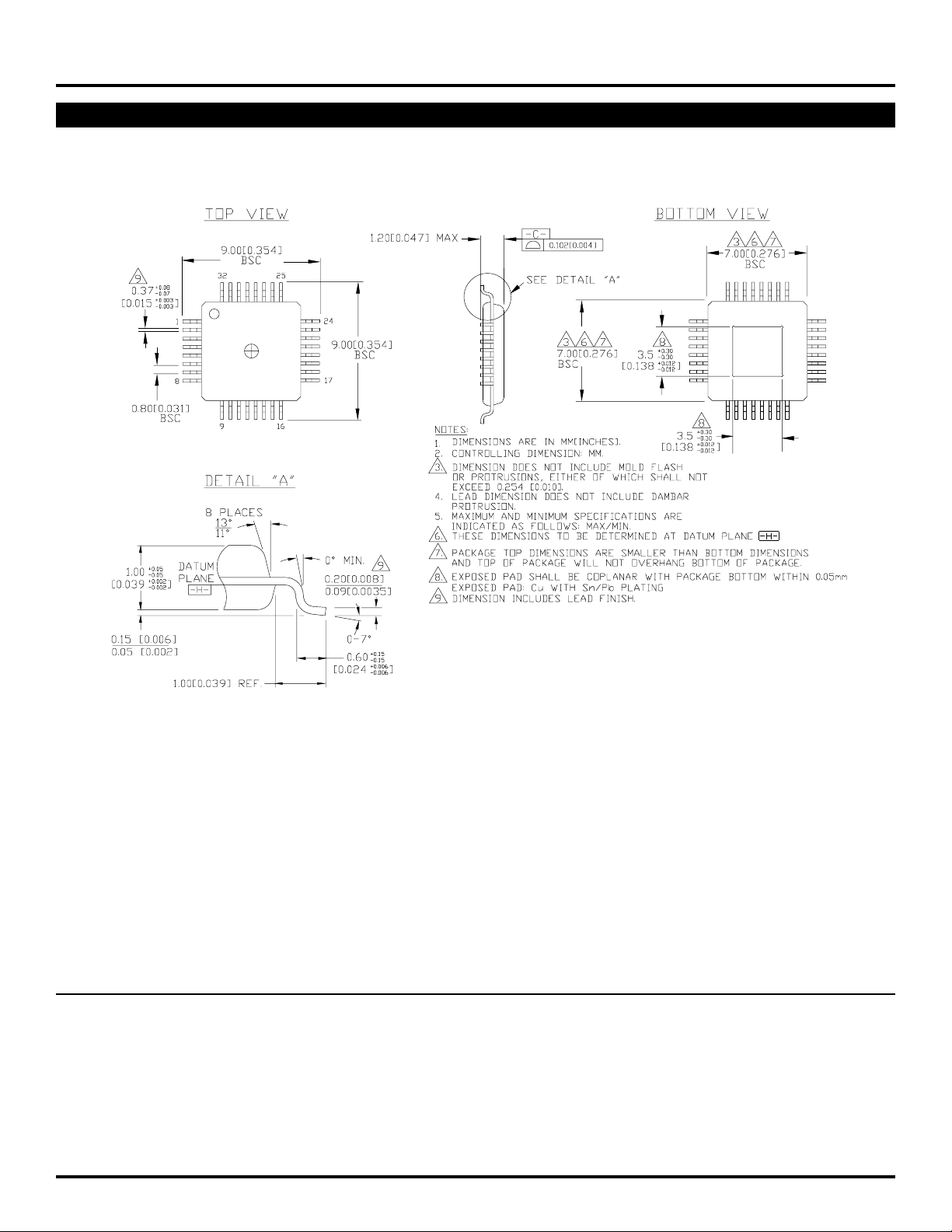
32 -PIN EPAD-TQFP (DIE UP) (H32-1)
SuperLite™
SY55858U
Rev. 01
MICREL, INC. 2180 FORTUNE DRIVE SAN JOSE, CA 95131 USA
The information furnished by Micrel in this datasheet is believed to be accurate and reliable. However, no responsibility is assumed by Micrel for its use.
Micrel reserves the right to change circuitry and specifications at any time without notification to the customer.
Micrel Products are not designed or authorized for use as components in life support appliances, devices or systems where malfunction of a product can
reasonably be expected to result in personal injury. Life support devices or systems are devices or systems that (a) are intended for surgical implant into
the body or (b) support or sustain life, and whose failure to perform can be reasonably expected to result in a significant injury to the user. A Purchaser’s
use or sale of Micrel Products for use in life support appliances, devices or systems is at Purchaser’s own risk and Purchaser agrees to fully indemnify
TEL + 1 (408) 944-0800 FAX + 1 (408) 474-1000 WEB http://www.micrel.com
Micrel for any damages resulting from such use or sale.
© 2005 Micrel, Incorporated.
M9999-110705
[email protected] or (408) 955-1690
8
 Loading...