

Page 1
SINGLE SUPPLY QUAD
PECL-TO-TTL W/LATCHED
OUTPUT ENABLE
ClockWorks™
SY10H841
SY100H841
FEATURES
■ Translates positive ECL to TTL (PECL-to-TTL)
■ 300ps pin-to-pin skew
■ 500ps part-to-part skew
■ Differential internal design for increased noise
immunity and stable threshold inputs
■ V
BB reference output
■ Single supply
■ Enable input
■ Latch enable input
■ Extra TTL and ECL power/ground pins to reduce
cross-talk/noise
■ High drive capability: 24mA each output
■ Fully compatible with industry standard 10K, 100K
I/O levels
■ Available in 16-pin SOIC package
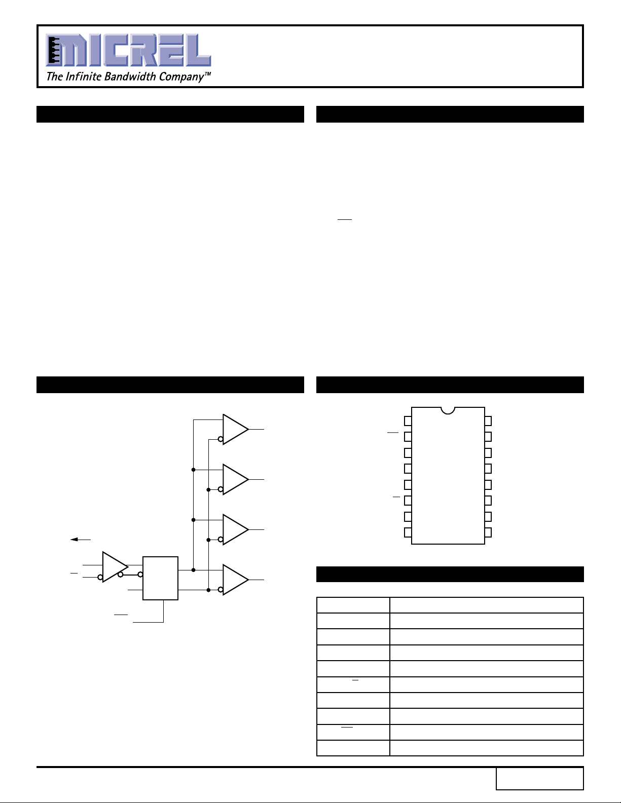
BLOCK DIAGRAM
DESCRIPTION
The SY10/100H841 are single supply, low skew
translating 1:4 clock drivers.
The devices feature a 24mA TTL output stage, with
AC performance specified into a 50pF load capacitance.
A latch is provided on-chip. When LEN is LOW (or left
open, in which case it is pulled low by the internal pulldowns) the latch is transparent. A HIGH on the enable
pin (EN) forces all outputs LOW.
As frequencies increase to 40MHz and above, precise
timing and shaping of clock signals becomes extremely
important. The H841 solves several clock distribution
problems such as minimizing skew (300ps), maximizing
clock fanout (24mA drive), and precise duty cycle control
through a proprietary differential internal design.
The 10K version is compatible with 10KH ECL logic
levels. The 100K version is compatible with 100K levels.
PIN CONFIGURATION
Q
0
Q
1
Q
V
BB
D
D
DQ
2
Q
3
PIN NAMES
LEN
V
116
2
EN
314
E
G
4
E
V
D
D
BB
T
G
SOIC
Z16-1
512
6
710
8
15
13
11
Q
3
T
G
Q
2
V
T
T
V
1
Q
G
T
9
Q
0
LEN
Pin Function
EN
GT TTL Ground (0V)
VT TTL VCC (+5.0V)
VE ECL VCC (+5.0V)
GE ECL Ground (0V)
D, D Signal Input (PECL)
VBB VBB Reference Output (PECL)
Q0 - Q3 Signal Outputs (TTL)
EN Enable Input (PECL)
LEN Latch Enable Input
Rev.: F Amendment: /0
1
Issue Date: May, 1999
Page 2
Micrel
ClockWorks™
SY10H841
SY100H841
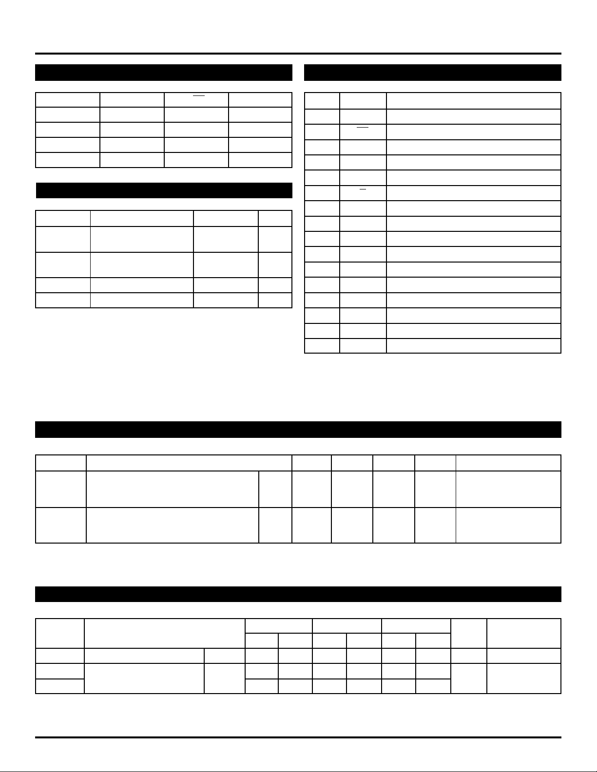
TRUTH TABLE
D LEN EN Q
LLLL
HLLH
XXHL
X H L Latch
ABSOLUTE MAXIMUM RATINGS
Symbol Rating Value Unit
E (ECL) Power Supply –0.5 to +7.0 V
V
VT (TTL) Voltage –0.5 to +7.0
V
I (ECL) Input Voltage 0.0 to VEE V
VOUT (TTL) 0.0 to VT
Tstore Storage Temperature –65 to +150 ˚C
TA Operating Temperature 0 to +85 ˚C
NOTE:
1. Permanent device damage may occur if ABSOLUTE MAXIMUM RATINGS
are exceeded. This is a stress rating only and functional operation is not
implied at conditions other than those detailed in the operational sections
of this data sheet. Exposure to ABSOLUTE MAXIMUM RATlNG conditions
for extended periods may affect device reliability.
(1)
PIN DESCRIPTION
Pin Symbol Description
1 LEN Latch Enable Input
2 EN Enable Input (PECL)
3GE ECL Ground (0V)
4VE ECL VCC (+5.0V)
5 D ECL Signal Input (Non-inverting)
6 D ECL Signal Input (Inverting)
7VBB VBB Reference Output (PECL)
8GT TTL Ground (0V)
9Q0 Signal Output (TTL)
10 GT TTL Ground (0V)
11 Q1 Signal Output (TTL)
12 VT TTL VCC (+5.0V)
13 VT TTL VCC (+5.0V)
14 Q2 Signal Output (TTL)
15 GT TTL Ground (0V)
16 Q
3 Signal Output (TTL)
VCC AND CLOAD
Ranges to meet duty cycle requirement: 0°C ≤ TA ≤ 85°C. Output duty cycle measured relative to 1.5V.
Symbol Parameter Min. Typ. Max. Unit Condition
W Ranges of VCC and CL to meet min. VCC 4.75 5.0 5.25 V All Outputs
P
pulse width (HIGH or LOW) at CL 10 — 50 pF
fOUT ≤ 40MHz PW 11 — — ns
W Ranges of VCC and CL to meet min. VCC 4.875 5.0 5.125 V All Outputs
P
pulse width (HIGH or LOW) at CL 15 — 27 pF
fOUT ≤ 50MHz PW 9.0 — — ns
DC CHARACTERISTICS
VT = VE = 5.0V ± 5%
TA = 0°CTA = +25°CTA = +85°C
Symbol Parameter Min. Max. Min. Max. Min. Max. Unit Condition
IEE Power Supply Current ECL — 40 — 40 — 40 mA VE Pin
CCH Power Supply Current TTL — 20 — 20 — 20 mA Total all VT pins
I
I
CCL —25—25—25
2
Page 3
ClockWorks™
Micrel
SY100H841
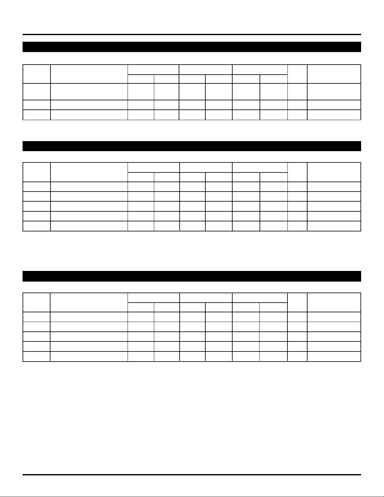
TTL DC ELECTRICAL CHARACTERISTICS
VT = VE = +5.0V ± 5%
TA = 0°CTA = +25°CTA = +85°C
Symbol Parameter Min. Max. Min. Max. Min. Max. Unit Condition
OH Output HIGH Voltage 2.5 — 2.5 — 2.5 — V IOH = –3.0mA
V
2.0 — 2.0 — 2.0 — IOH = –15mA
VOL Output LOW Voltage — 0.5 — 0.5 — 0.5 V IOL = 24mA
I
OS Output Short Circuit Current –80 –200 –80 –200 –80 –200 mA VOUT = 0V
SY10H841
10H ECL DC ELECTRICAL CHARACTERISTICS
(1)
VT = VE = +5.0V ± 5%
TA = 0°CTA = +25°CTA = +85°C
Symbol Parameter Min. Max. Min. Max. Min. Max. Unit Condition
IIH Input HIGH Current — 225 — 175 — 175 µA—
IIL Input LOW Current 0.5 — 0.5 — 0.5 — µA—
VIH Input HIGH Voltage 3.830 4.160 3.870 4.190 3.940 4.280 V VE = 5.0V
VIL Input LOW Voltage 3.050 3.520 3.050 3.520 3.050 3.555 V VE = 5.0V
BB Output Reference Voltage 3.620 3.730 3.650 3.750 3.690 3.810 V VE = 5.0V
V
NOTE:
1. ECL VIH, VIL and VBB are referenced to VCCE and will vary 1:1 with the power supply. The levels shown are for IVT = IVO = VCCE = +5.0V.
100H ECL DC ELECTRICALCHARACTERISTICS
(1)
VT = VE = +5.0V ± 5%
TA = 0°CTA = +25°CTA = +85°C
Symbol Parameter Min. Max. Min. Max. Min. Max. Unit Condition
IIH Input HIGH Current — 225 — 175 — 175 µA—
IIL Input LOW Current 0.5 — 0.5 — 0.5 — µA—
VIH Input HIGH Voltage 3.835 4.120 3.835 4.120 3.835 4.120 V VE = 5.0V
VIL Input LOW Voltage 3.190 3.525 3.190 3.525 3.190 3.525 V VE = 5.0V
V
BB Output Reference Voltage 3.620 3.740 3.620 3.740 3.620 3.740 V VE = 5.0V
NOTE:
1. ECL VIH, VIL and VBB are referenced to VCCE and will vary 1:1 with the power supply. The levels shown are for IVT = IVO = VCCE = +5.0V.
3
Page 4
ClockWorks™
SY10H841
Micrel
SY100H841
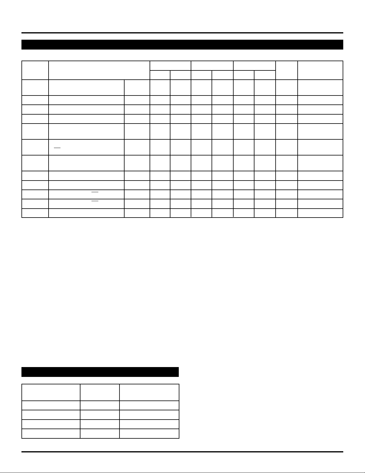
AC CHARACTERISTICS
VT = VE = 5.0V ± 5%
TA = 0°CTA = +25°CTA = +85°C
Symbol Parameter Min. Max. Min. Max. Min. Max. Unit Condition
PLH Propagation Delay Q0–Q3 2.7 3.7 2.7 3.7 2.7 3.7 ns CL = 50pF
t
tPHL D to Output
tskpp Part-to-Part Skew
tskew++ Within-Device Skew
tskew– – Within-Device Skew
PLH Propagation Delay Q0–Q3 2.7 3.7 2.7 3.7 2.7 3.7 ns CL = 50pF
t
tPHL LEN to Q
PLH Propagation Delay Q0–Q3 2.7 3.7 2.7 3.7 2.7 3.7 ns CL = 50pF
t
tPHL EN to Output
r Output Rise/Fall Time Q0–Q3 — 1.5 — 1.5 — 1.5 ns CL = 50pF
t
tf 1.0V to 2.0V
fMAX Max. Input Frequency
— Pulse Width Q0–Q3 1.5 — 1.5 — 1.5 — ns —
— Recovery Time EN Q0–Q3 1.0 — 1.0 — 1.0 — ns —
tS Set-up Time D, EN Q0–Q3 0.75 — 0.75 — 0.75 — ns —
H Hold Time D, EN Q0–Q3 0.75 — 0.75 — 0.75 — ns —
t
NOTES:
1. Device-to-Device Skew considering HIGH-to-HIGH transitions at common VCC level.
2. Within-Device Skew considering HIGH-to-HIGH transitions at common VCC level.
3. Within-Device Skew considering LOW-to-LOW transitions at common VCC level.
4. All skew parameters are guaranteed but not tested.
5. Frequency at which output levels will meet at 0.8V to 2.0V minimum swing.
6. The fMAX value is specified as the minimum guaranteed maximum frequency. Actual operational maximum frequency may be greater.
(1,4)
(2,4)
(3,4)
(5,6)
Q0–Q3 — 0.5 — 0.5 — 0.5 ns CL = 50pF
Q0–Q3 — 0.3 — 0.3 — 0.3 ns CL = 50pF
Q0–Q3 — 0.3 — 0.3 — 0.3 ns CL = 50pF
Q0–Q3 160 — 160 — 160 — MHz CL = 50pF
LOGIC DIAGRAMPRODUCT ORDERING CODE
Ordering Package Operating
Code Type Range
SY10H841ZC Z16-1 Commercial
SY10H841ZCTR Z16-1 Commercial
SY100H841ZC Z16-1 Commercial
SY100H841ZCTR Z16-1 Commercial
4
Page 5
Micrel
–
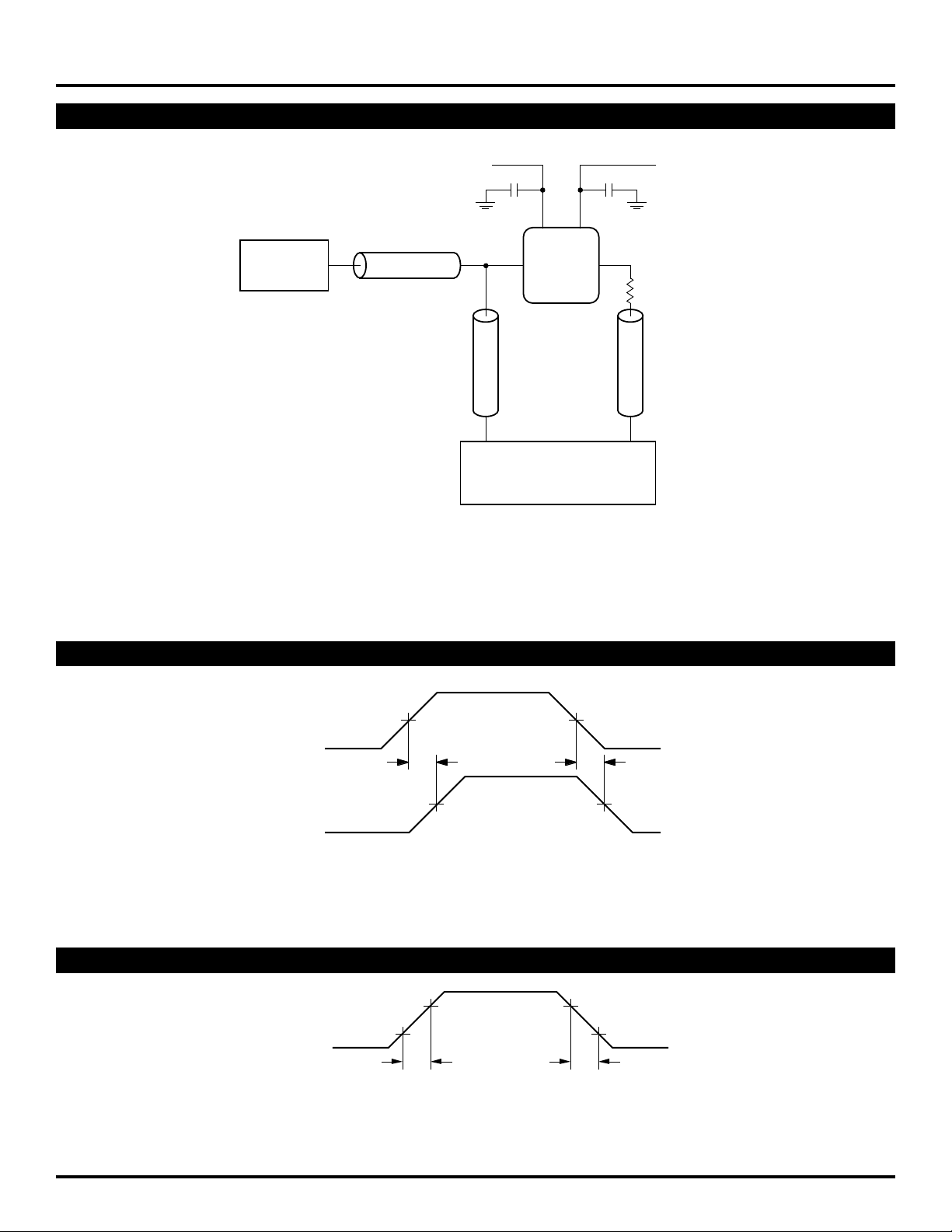
TTL SWITCHING CIRCUIT
GENERATOR
USE 0.1µF CAPACITORS
FOR DECOUPLING.
50Ω COAX
PULSE
V
EE
PECL
DEVICE
IN OUT
50Ω COAX 50Ω COAX
VCC & V
UNDER
TEST
ClockWorks™
SY10H841
SY100H841
CCO
TTL
450Ω
USE OSCILLOSCOPE
INTERNAL 50Ω LOAD
FOR TERMINATION.
CH A
OSCILLOSCOPE
ECL/TTL PROPAGATION DELAY — SINGLE ENDED
50%
VIN
pd++ Tpd–
T
1.5V
VOUT
CH B
ECL/TTL WAVEFORMS: RISE AND FALL TIMES
V
OUT
T
rise
2.0V
0.8V
T
fall
5
Page 6
Micrel
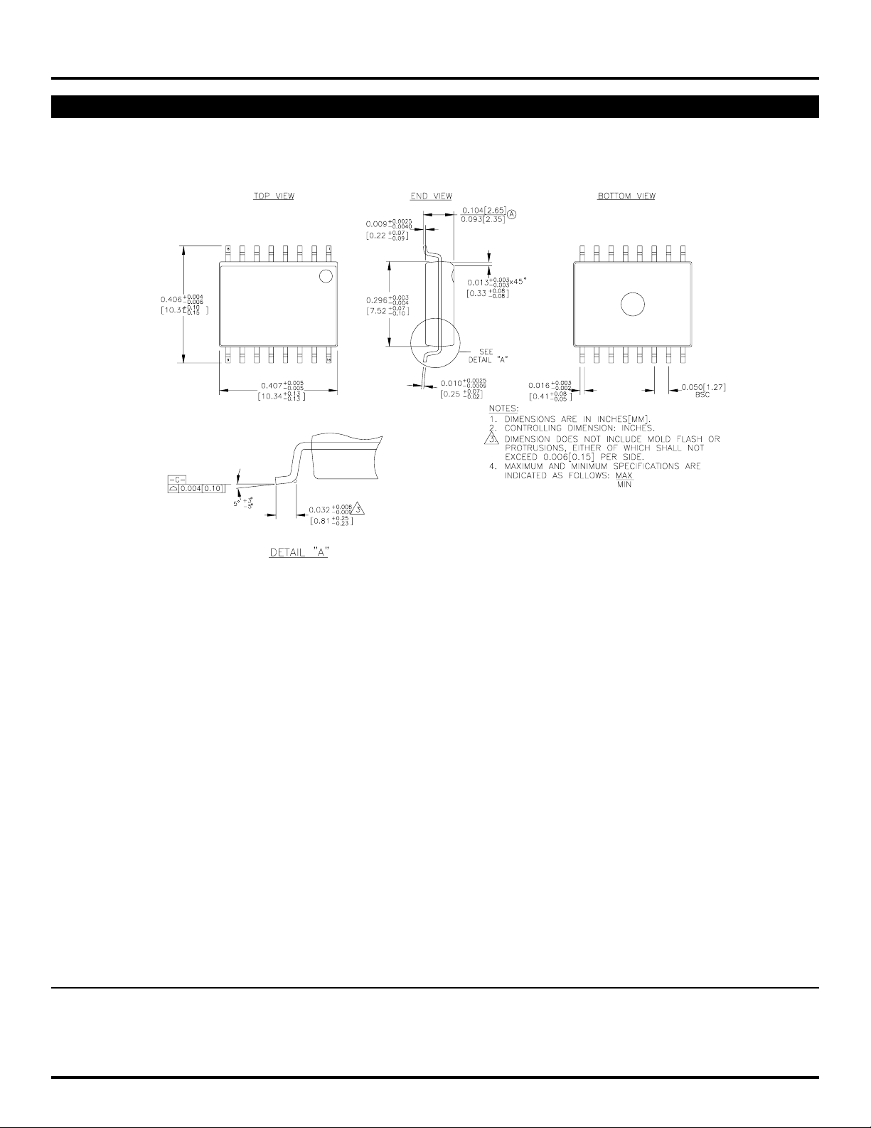
16 LEAD SOIC .300" WIDE (Z16-1)
ClockWorks™
SY10H841
SY100H841
Rev. 03
MICREL-SYNERGY 3250 SCOTT BOULEVARD SANTA CLARA CA 95054 USA
TEL + 1 (408) 980-9191 FAX + 1 (408) 914-7878 WEB http://www.micrel.com
This information is believed to be accurate and reliable, however no responsibility is assumed by Micrel for its use nor for any infringement of patents or
other rights of third parties resulting from its use. No license is granted by implication or otherwise under any patent or patent right of Micrel Inc.
© 2000 Micrel Incorporated
6
 Loading...