

Page 1
REGISTERED HEX
TTL-TO-PECL
SY10H606
SY100H606
FEATURES
■ Differential 50Ω ECL outputs
■ Choice between differential PECL or TTL clock input
■ Single +5V power supply
■ VBB output for single-ended use
■ Multiple power and ground pins to minimize noise
■ Specified within-device skew
■ Fully compatible with Motorola MC10H/100H606
■ Available in 28-pin PLCC package
DESCRIPTION
The SY10/100H606 are 6-bit, registered, single supply
TTL-to-PECL translators. The devices feature differential
PECL outputs as well as a choice between either a
differential PECL clock input or a TTL clock input. The
asynchronous master reset control is a PECL level input.
With its differential ECL outputs and TTL inputs, the
H606 device is ideally suited for the transmit function of
a HPPI bus-type board-to-board interface application. The
on-chip registers simplify the task of synchronizing the
data between the two boards.
The device is available in either ECL standard: the
10H device is compatible with 10K logic levels, while the
100H device is compatible with 100K logic levels.
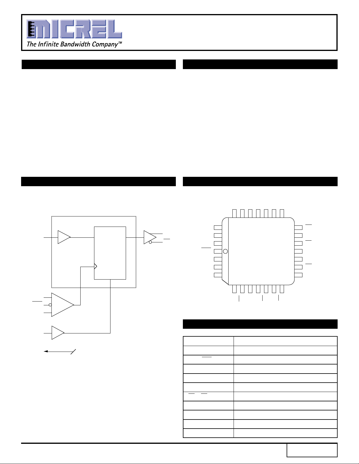
BLOCK DIAGRAM PIN CONFIGURATION
2
D1D
25
1 OF 6 BITS
D
Q
D
n
DQ
n
Q
n
TCLK
V
BB
0
CLK
CLK
CLK
R
V
MR
CCE
24 23 22 21 20 19
26
27
28
1
2
3
4
TOP VIEW
567891011
CCT
V
D3D4D
PLCC
5
CCE
V
18
Q
5
17
Q
5
16
Q
4
15
Q
4
14
V
CCE
13
Q
3
12
Q
3
CLK
CLK
TCLK
MR
V
BB
1
0
0
Q
Q
2
1
Q
2
Q
Q
Q
GND
PIN NAMES
Pin Function
D0 – D5 TTL Data Inputs
CLK, CLK Differential PECL Clock Inputs
TCLK TTL Clock Input
MR PECL Master Reset Input
Q0 – Q5 True PECL Outputs
Q0 – Q5 Inverted PECL Outputs
VCCE PECL VCC (5.0V)
VCCT TTL VCC (5.0V)
GND TTL/PECL Ground
BB VBB Reference Output (PECL)
V
1
Rev.: D Amendment: /0
Issue Date: March, 1998
Page 2
SY10H606
Micrel
SY100H606
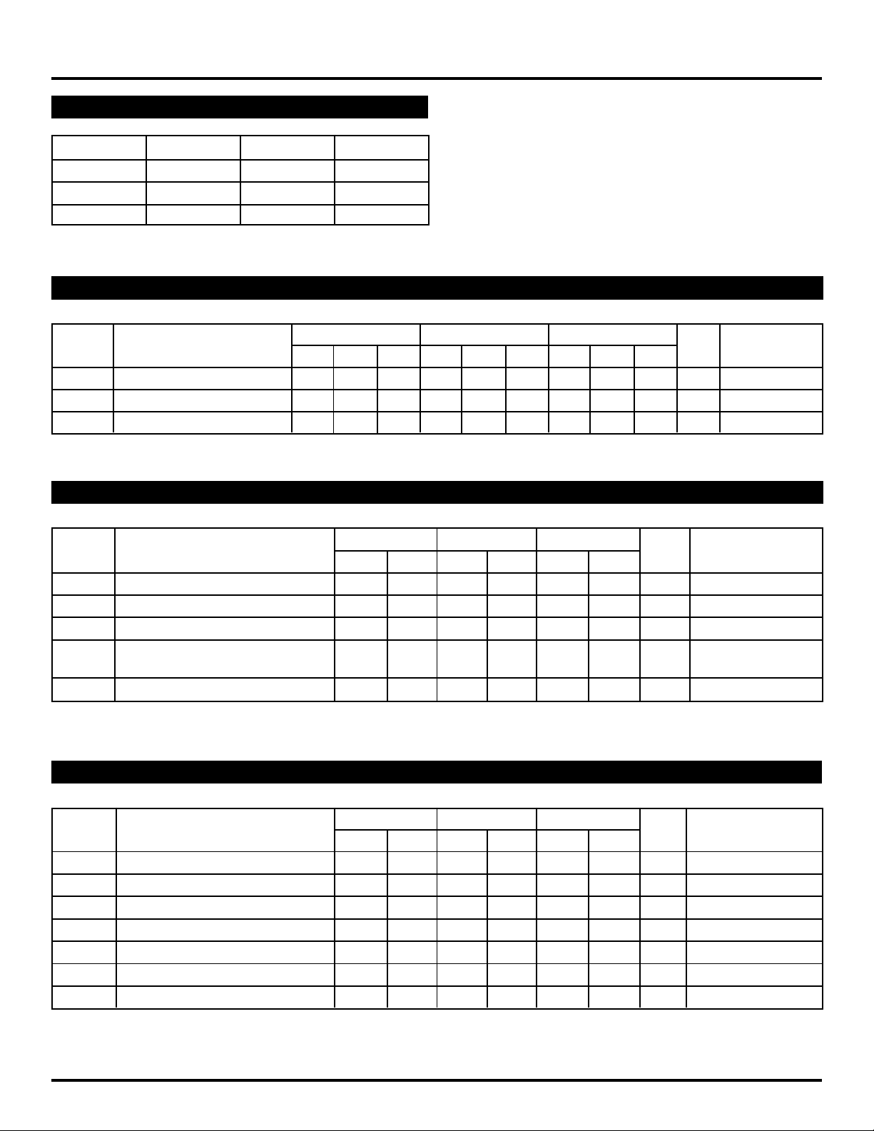
TRUTH TABLE
Dn MR TCLK/CLK Qn + 1
LLZL
HLZH
XHXL
Z = Low to High Transition.
DC ELECTRICAL CHARACTERISTICS
VCCT = VCCE = 5.0V ±5%
TA= 0°CTA= +25°CTA= + 85°C
Symbol Parameter Min. Typ. Max. Min. Typ. Max. Min. Typ. Max. Unit Condition
ICCTL Supply Current — 18 30 — 18 30 — 18 30 mA Outputs LOW
ICCTH Supply Current — 13 25 — 13 25 — 13 25 mA Outputs HIGH
GND Supply Current — 75 90 — 75 90 — 75 95 mA
I
TTL DC ELECTRICAL CHARACTERISTICS
VCCT = VCCE = 5.0V ±5%
TA= 0°CTA= +25°CTA= + 85°C
Symbol Parameter Min. Max. Min. Max. Min. Max. Unit Condition
VIH Input HIGH Voltage 2.0 — 2.0 — 2.0 — V
VIL Input LOW Voltage — 0.8 — 0.8 — 0.8 V
VIK Input Clamp Voltage —–1.2 —–1.2 —–1.2 V IIN = –18mA
IH Input HIGH Current — 20 — 20 — 20 µAVIN = 2.7V
I
— 100 — 100 — 100 VIN = 7.0V
IL Input LOW Current —–0.6 —–0.6 —–0.6 mA VIN = 0.5V
I
10H PECL DC ELECTRICAL CHARACTERISTICS
VCCT = VCCE = 5.0V ±5%
TA= 0°CTA= +25°CTA= + 85°C
Symbol Parameter Min. Max. Min. Max. Min. Max. Unit Condition
IIH Input HIGH Current — 225 — 145 — 145 µA
IIL Input LOW Current 0.5 — 0.5 — 0.5 — µA
VIH Input HIGH Voltage 3830 4160 3870 4190 3930 4280 mV VCCT = 5.0V
VIL Input LOW Voltage 3050 3520 3050 3520 3050 3555 mV VCCT = 5.0V
VOH Output HIGH Voltage 3980 4160 4020 4190 4080 4270 mV VCCT = 5.0V
VOL Output LOW Voltage 3050 3370 3050 3370 3050 3400 mV VCCT = 5.0V
BB Output Bias Voltage 3620 3730 3650 3750 3690 3810 mV VCCT = 5.0V
V
NOTE:
1. PECL VIL, VIH, VOL, VOH, VBB are given for VCCT = VCCE = 5.0V and will vary 1:1 with power supply.
(1)
2
Page 3
Micrel
SY10H606
SY100H606
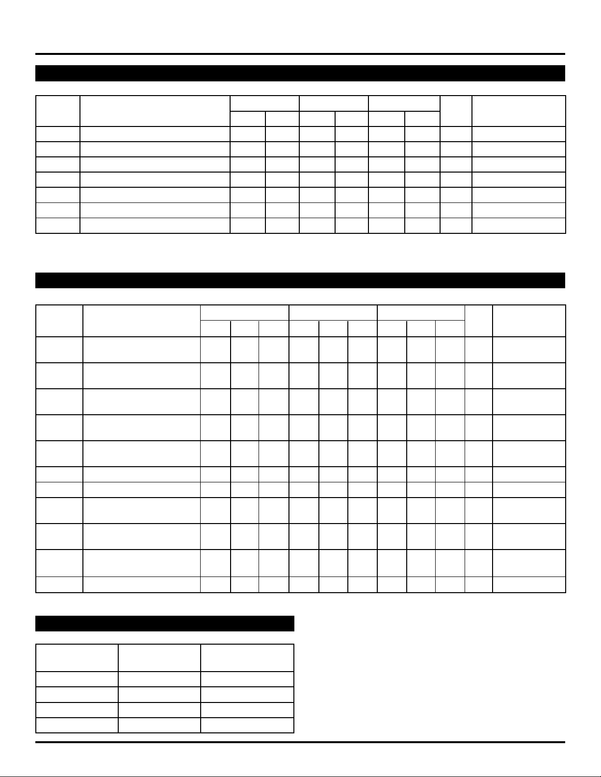
100H PECL DC ELECTRICAL CHARACTERISTICS
(1)
VCCT = VEEC = 5.0V ±5%
TA= 0°CTA= +25°CTA= + 85°C
Symbol Parameter Min. Max. Min. Max. Min. Max. Unit Condition
IIH Input HIGH Current — 225 — 145 — 145 µA
IIL Input LOW Current 0.5 — 0.5 — 0.5 — µA
VIH Input HIGH Voltage 3835 4120 3835 4120 3835 4120 mV VCCT = 5.0V
VIL Input LOW Voltage 3190 3525 3190 3525 3190 3525 mV VCCT = 5.0V
VOH Output HIGH Voltage 3975 4120 3975 4120 3975 4120 mV VCCT = 5.0V
VOL Output LOW Voltage 3190 3380 3190 3380 3190 3380 mV VCCT = 5.0V
V
BB Output Bias Voltage 3620 3740 3620 3740 3620 3740 mV VCCT = 5.0V
NOTE:
1. PECL VIL, VIH, VOL, VOH, VBB are given for VCCT = VCCE = 5.0V and will vary 1:1 with power supply.
AC ELECTRICAL CHARACTERISTICS
VCCT = VCCE = 5.0V ±5%
TA= 0°CTA= +25°CTA= + 85°C
Symbol Parameter Min. Typ. Max. Min. Typ. Max. Min. Typ. Max. Unit Condition
PD Propagation Delay 0.800 — 2.800 0.800 — 2.800 0.800 — 2.800 ns
t
TCLK+ +
PD Propagation Delay 0.800 — 2.800 0.800 — 2.800 0.800 — 2.800 ns
t
TCLK+ –
t
PD Propagation Delay 0.800 — 2.800 0.800 — 2.800 0.800 — 2.800 ns
CLK+ +
PD Propagation Delay 0.800 — 2.800 0.800 — 2.800 0.800 — 2.800 ns
t
CLK+ –
PD Propagation Delay 0.800 — 2.800 0.800 — 2.800 0.800 — 2.800 ns
t
MR+ –
tS Set-up Time 1.5 0.5 — 1.5 0.5 — 1.5 0.5 — ns
tH Hold Time1.5 0.5 — 1.5 0.5 — 1.5 0.5 — ns
t
PW Minimum Pulse Width 1.5 ——1.5 1.0 — 1.5 ——ns
CLK
PW Minimum Pulse Width 1.5 ——1.5 ——1.5 ——ns
t
MR
tr
tf
tRES/REC Reset/Recovery Time 2.5 2.0 — 2.5 2.0 — 2.5 2.0 — ns
Rise/Fall Time ——2.0 — 1.0 2.0 ——2.0 ns
PRODUCT ORDERING CODE
Ordering Package Operating
Code Type Range
SY10H606JC J28-1 Commercial
SY10H606JCTR J28-1 Commercial
SY100H606JC J28-1 Commercial
SY100H606JCTR J28-1 Commercial
3
Page 4
Micrel
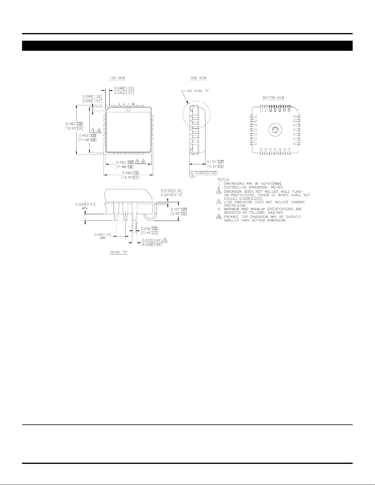
28 LEAD PLCC (J28-1)
SY10H606
SY100H606
Rev. 03
MICREL-SYNERGY 3250 SCOTT BOULEVARD SANTA CLARA CA 95054 USA
TEL + 1 (408) 980-9191 FAX + 1 (408) 914-7878 WEB http://www.micrel.com
This information is believed to be accurate and reliable, however no responsibility is assumed by Micrel for its use nor for any infringement of patents or
other rights of third parties resulting from its use. No license is granted by implication or otherwise under any patent or patent right of Micrel Inc.
© 2000 Micrel Incorporated
4
 Loading...