

Page 1

TRIPLE LVPECL-TO-PECL
B
B
B
2
0
0
OR PECL-TO-LVPECL
TRANSLATOR
SY100EL92
FEATURES
■ 5V and 3.3V power supplies required
■ Also, supports LVPECL-to-PECL translation
■ 500ps propagation delays
■ Fully differential design
■ Differential line receiver capability
■ Application note
■ Available in 20-pin SOIC package
PIN CONFIGURATION/BLOCK DIAGRAM
19
18
17
16
15
14
13
12
20
V
Q
Q
V
Q
Q
V
Q
Q
V
CC
0
0
CCO
1
1
CCO
2
2
CC
V
CC_VB
1
2
D
3
D
4
V
B
5
D
1
D
1
6
7
V
B
8
D
D
2
9
GND
10 11
SOIC
TOP VIEW
DESCRIPTION
The SY100EL92 is a triple LVPECL-to-PECL or PECLto-LVPECL translator. The device receives standard PECL
signals and translates them to differential LVPECL output
signals (or vice versa). SY100EL92 can also be used as a
differential line receiver for PECL-to-PECL or LVPECL-toLVPECL signals. However, please note that for the latter
we will need two different power supplies. Please refer to
Function Table for more details.
VBB outputs are provided for interfacing single ended
input signals. If a single ended input is to be used, the VBB
output should be connected to the D input and the active
signal will drive the D input. When used, the VBB should be
bypassed to VCC via a 0.01µF capacitor. The VBB is
designed to act as a switching reference for the SY100EL92
under single ended input conditions. As a result, the pin
can only source/sink 0.5mA of current.
To accomplish the PECL-to-LVPECL level translation,
the SY100EL92 requires three power rails. The VCC and
VCC_VBB supply is to be connected to the standard PECL
supply, the 3.3V supply is to be connected to the VCCO
supply, and GND is connected to the system ground plane.
Both the VCC and VCCO should be bypassed to ground with
a 0.01µF capacitor.
To accomplish the LVPECL-to-PECL level translation,
the SY100EL92 requires three power rails as well. The 5.0V
supply is connected to the VCC and VCCO pins, 3.3V supply
is connected to the VCC_VBB pin and GND is connected to
the system ground plane. VCC_VBB is used to provide a
proper VBB output level if a single ended input is used. For
differential LVPECL input VCC_VBB can be either 3.3V or
5V.
Under open input conditions, the D input will be biased
at a VCC/2 voltage level and the D input will be pulled to
GND. This condition will force the "Q" output low, ensuring
stability.
FUNCTION TABLE
Function Vcc Vcco Vcc_VBB
PECL-to-LVPECL 5.0V 3.3V 5.0V
LVPECL-to-PECL 5.0V 5.0V 3.3V
PECL-to-PECL 5.0V 5.0V 5.0V
LVPECL-to-LVPECL 5.0V 3.3V 3.3V
PIN NAMES
Pin Function
Dn PECL / LVPECL Inputs
Qn PECL / LVPECL Outputs
VBB PECL / LVPECL Reference Voltage Output
VCCO VCC for Output
VCC_VBB VCC for VBB Output
GND Common Ground Rail
V
CC VCC for Internal Circuitry
Rev.: D Amendment: /0
1
Issue Date: January, 1999
Page 2

Micrel
SY100EL92
PECL INPUT DC ELECTRICAL CHARACTERISTICS
VCC_VBB = VCC = +4.5V to +5.5V; VCCO = +3.0V to +3.8V
TA = –40°CTA = 0°CTA = +25°CTA = +85°C
Symbol Parameter Min. Typ. Max. Min. Typ. Max. Min. Typ. Max. Min. Typ. Max. Unit
VCC Power Supply Voltage 4.5 — 5.5 4.5 — 5.5 4.5 — 5.5 4.5 — 5.5 V
VIH Input HIGH Voltage
VIL Input LOW Voltage
VPP Minimum Peak-to-Peak 150 — — 150 — — 150 — — 150 — — mV
Input
IIH Input HIGH Current — — 150 — — 150 — — 150 — — 150 µA
IIL Input LOW Current Dn 0.5 — — 0.5 — — 0.5 — — 0.5 — — µA
VBB Output Reference
CC Power Supply Current — — 12 — — 12 — 8.0 12 — — 12 mA
I
NOTE:
1. These levels are for VCC_VBB = 5.0V. Level specifications will vary 1:1 with VCC_VBB.
(1)
(1)
3.835 — 4.120 3.835 — 4.120 3.835 — 4.120 3.835 — 4.120 V
3.190 — 3.515 3.190 — 3.525 3.190 — 3.525 3.190 — 3.525 V
Dn –600 — — –600 — — –600 — — –600 — —
(1)
3.620 — 3.740 3.620 — 3.740 3.620 — 3.740 3.620 — 3.740 V
LVPECL OUTPUT DC ELECTRICAL CHARACTERISTICS
VCC_VBB = VCC = +4.5V to +5.5V; VCCO = +3.0V to +3.8V
TA = –40°CTA = 0°CTA = +25°CTA = +85°C
Symbol Parameter Min. Typ. Max. Min. Typ. Max. Min. Typ. Max. Min. Typ. Max. Unit
VCCO Power Supply Voltage 3.0 — 3.8 3.0 — 3.8 3.0 3.3 3.8 3.0 — 3.8 V
VOH Output HIGH Voltage
VOL Output LOW Voltage
CCO Power Supply Current — — 20 — — 20 — 15 20 — — 21 mA
I
NOTE:
1. These levels are for VCCO = 3.3V. Level specifications will vary 1:1 with VCCO.
(1)
2.215 — 2.420 2.275 — 2.420 2.275 2.350 2.420 2.275 — 2.420 V
(1)
1.470 — 1.745 1.490 — 1.680 1.490 1.600 1.680 1.490 — 1.680 V
LVPECL INPUT DC ELECTRICAL CHARACTERISTICS
VCC_VBB = +3.0V to +3.8V
Symbol Parameter Min. Typ. Max. Min. Typ. Max. Min. Typ. Max. Min. Typ. Max. Unit
VCC Power Supply Voltage 4.5 — 5.5 4.5 — 5.5 4.5 — 5.5 4.5 — 5.5 V
VIH Input HIGH Voltage
VIL Input LOW Voltage
VPP Minimum Peak-to-Peak 150 — — 150 — — 150 — — 150 — — mV
Input
IIH Input HIGH Current — — 150 — — 150 — — 150 — — 150 µA
IIL Input LOW Current Dn 0.5 — — 0.5 — — 0.5 — — 0.5 — — µA
VBB Output Reference
CC Power Supply Current — — 12 — — 12 — 8.0 12 — — 12 mA
I
NOTES:
1. VCC_VBB = 3.3V is only required for single-ended LVPECL input. For differential LVPECL input, VCC_VBB can be either 3.3V or 5V.
2. These levels are for VCC_VBB = 3.3V. Level specifications will vary 1:1 with VCC_VBB.
(1)
; VCC = VCCO = +4.5V to +5.5V
TA = –40°CTA = 0°CTA = +25°CTA = +85°C
(2)
(2)
2.135 — 2.420 2.135 — 2.420 2.135 — 2.420 2.135 — 2.420 V
1.490 — 1.825 1.490 — 1.825 1.490 — 1.825 1.490 — 1.825 V
Dn –600 — — –600 — — –600 — — –600 — —
(2)
1.92 — 2.04 1.92 — 2.04 1.92 — 2.04 1.92 — 2.04 V
2
Page 3
Micrel
SY100EL92
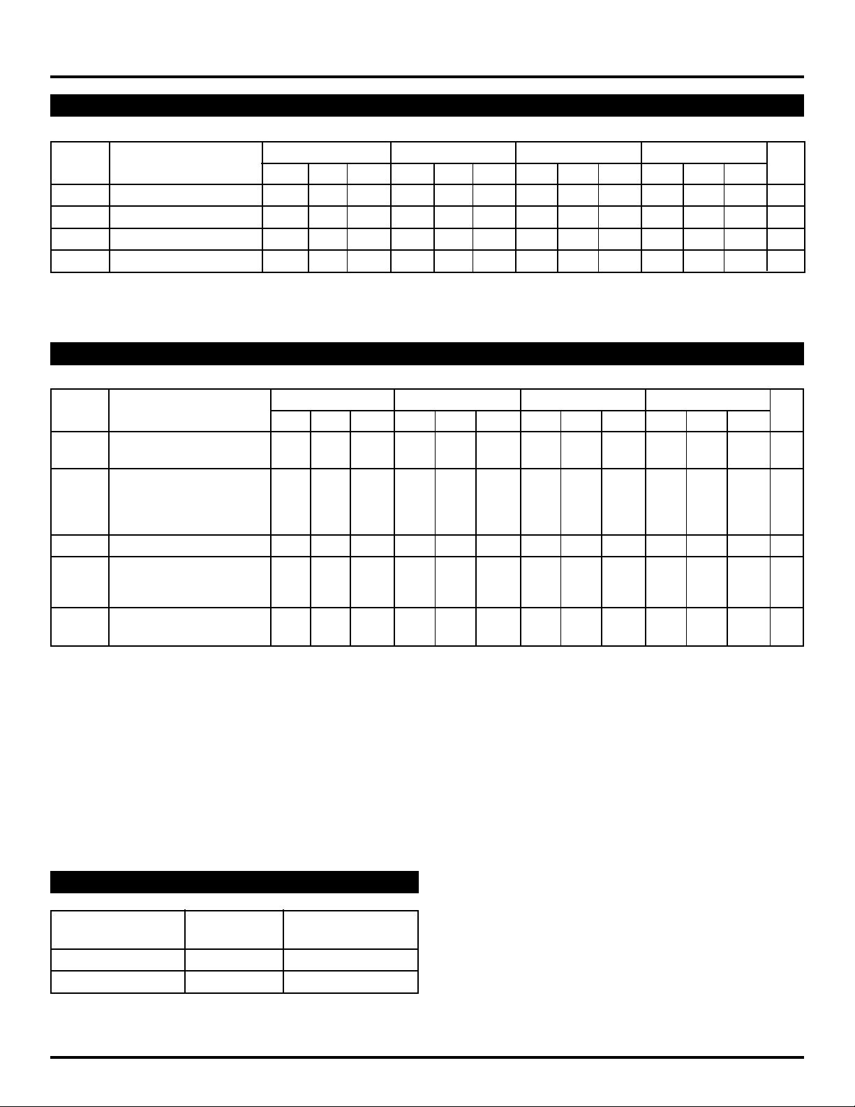
PECL OUTPUT DC ELECTRICAL CHARACTERISTICS
VCC_VBB = +3.0V to +3.8V; VCC = VCCO = +4.5V to +5.5V
TA = –40°CTA = 0°CTA = +25°CTA = +85°C
Symbol Parameter Min. Typ. Max. Min. Typ. Max. Min. Typ. Max. Min. Typ. Max. Unit
VCCO Power Supply Voltage 4.5 — 5.5 4.5 — 5.5 4.5 — 5.5 4.5 — 5.5 V
VOH Output HIGH Voltage
VOL Output LOW Voltage
ICCO Power Supply Current — — 20 — — 20 — 15 20 — — 21 mA
NOTE:
1. These levels are for VCCO = 5.0V. Level specifications will vary 1:1 with VCCO.
(1)
3.915 — 4.120 3.975 — 4.120 3.975 — 4.120 3.975 — 4.120 V
(1)
3.170 — 3.445 3.190 — 3.380 3.190 — 3.380 3.190 — 3.380 V
AC ELECTRICAL CHARACTERISTICS
(1)
TA = –40°CTA = 0°CTA = +25°CTA = +85°C
Symbol Parameter Min. Typ. Max. Min. Typ. Max. Min. Typ. Max. Min. Typ. Max. Unit
t
PLH Propagation Delay Diff. 430 520 630 430 520 630 430 520 630 430 520 630 ps
tPHL D to Q S.E. 410 540 710 410 540 710 410 540 710 410 540 710
t
skew Within-Device Skew
Output-to-Output
Part-to-Part (Diff.)
Duty Cycle (Diff.)
VPP Minimum Input Swing
VCMR Common Mode Range
(2)
(3)
(2)
(4)
— 20 100 — 20 100 — 20 100 — 20 100 ps
— 20 200 — 20 200 — 20 200 — 20 200
—25——25——25——25—
150 — — 150 — — 150 — — 150 — — mV
(5)
V
VPP < 500mV 1.3 — VCC–0.2 1.2 — VCC–0.2 1.2 — VCC–0.2 1.2 — VCC–0.2
VPP ≥ 500mV 1.5 — VCC–0.2 1.4 — VCC–0.2 1.4 — VCC–0.2 1.4 — VCC–0.2
tr Output Rise/Fall Times Q 320 — 580 320 — 580 320 — 580 320 — 580 ps
tf (20% to 80%)
NOTES:
1. Power supply requirements applies as indicated in the DC electrical characteristics tables.
2. Skew is measured between outputs under identical transitions.
3. Duty cycle skew is the difference between a TPLH and TPHL propagation delay through a device Common Mode Range.
4. Minimum input swing for which AC parameters are guaranteed. The device has a DC gain of ~40.
5. The CMR range is referenced to the most positive side of the differential input signal. Normal operation is obtained if the HIGH level falls within the specified
range and the peak-to-peak voltage lies between VPP min. and 1V.
PRODUCT ORDERING CODE
Ordering Package Operating
Code Type Range
SY100EL92ZC Z20-1 Commercial
SY100EL92ZCTR Z20-1 Commercial
3
Page 4
Micrel
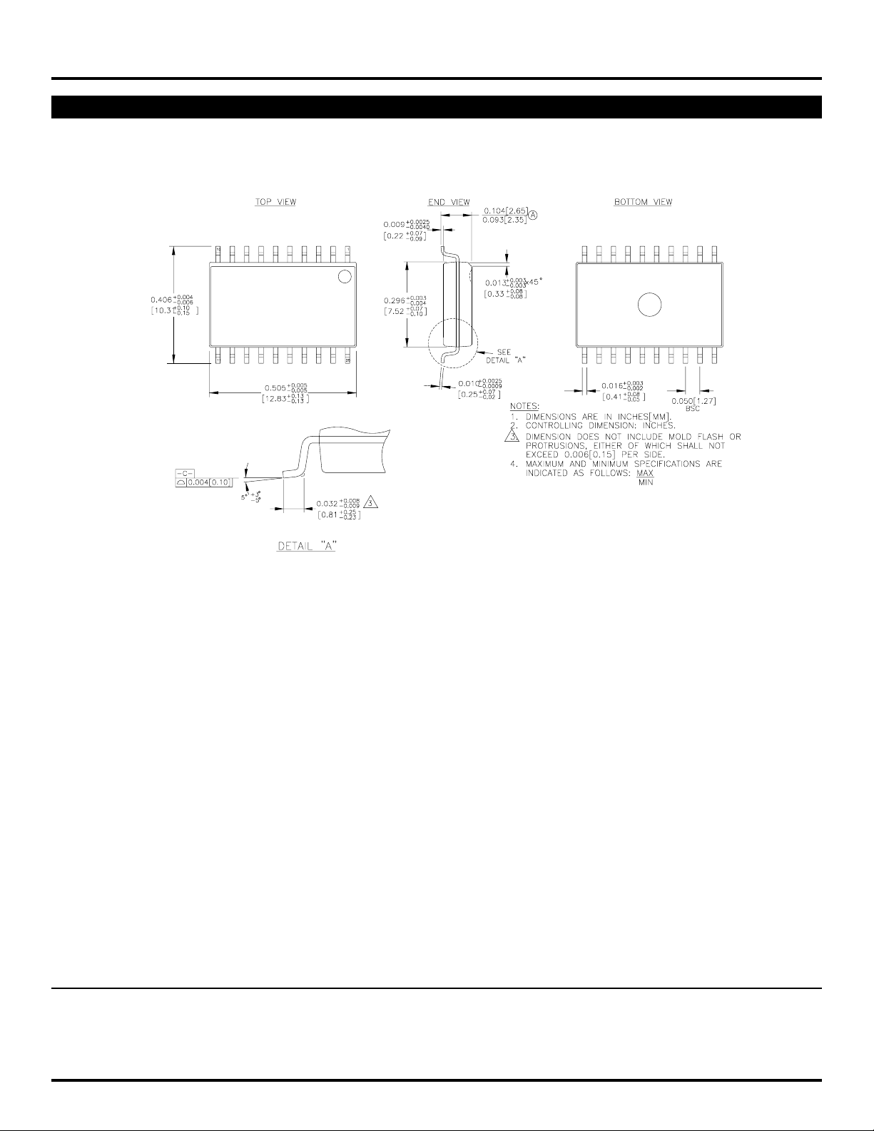
20 LEAD SOIC .300" WIDE (Z20-1)
SY100EL92
Rev. 03
MICREL-SYNERGY 3250 SCOTT BOULEVARD SANTA CLARA CA 95054 USA
TEL + 1 (408) 980-9191 FAX + 1 (408) 914-7878 WEB http://www.micrel.com
This information is believed to be accurate and reliable, however no responsibility is assumed by Micrel for its use nor for any infringement of patents or
other rights of third parties resulting from its use. No license is granted by implication or otherwise under any patent or patent right of Micrel Inc.
© 2000 Micrel Incorporated
4
 Loading...