

Page 1
4-BIT SERIAL-to-PARALLEL
CONVERTER
SY10E445
SY100E445
FEATURES
■ On-chip clock ÷4 and ÷8
■ Extended 100E VEE range of –4.2V to –5.5V
■ 2.5Gb/s data rate capability
■ Differential clock and serial inputs
■ VBB output for single-ended use
■ Asynchronous data synchronization
■ Mode select to expand to 8 bits
■ Internal 75kΩ input pull-down resistors
■ Fully compatible with Motorola MC10E/100E445
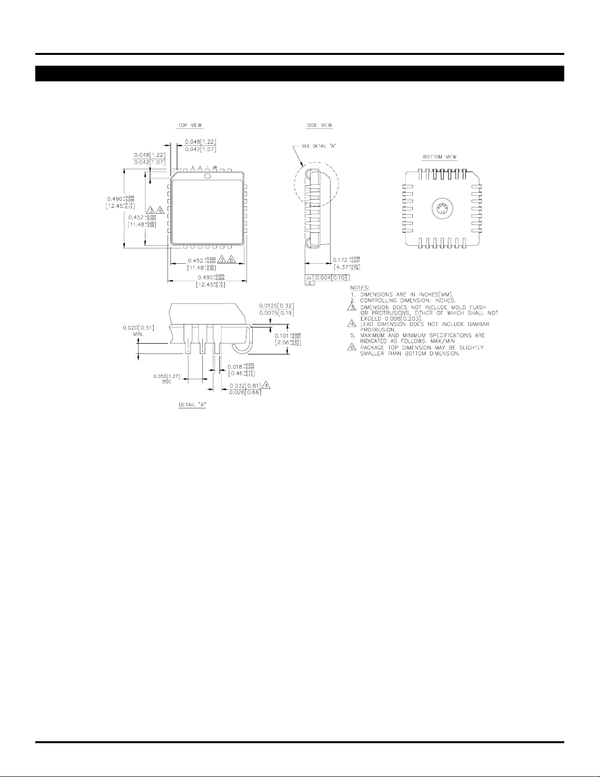
■ Available in 28-pin PLCC package
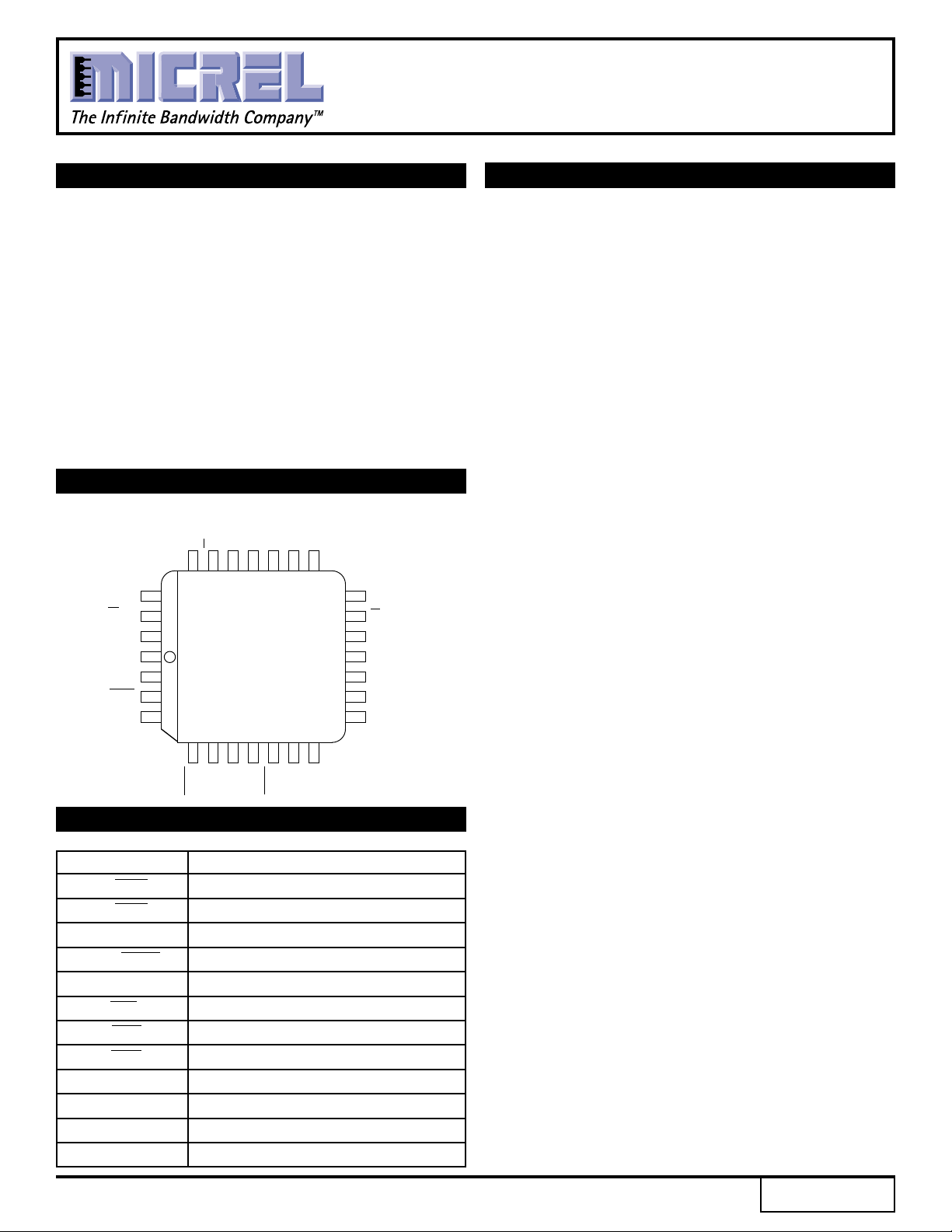
PIN CONFIGURATION
SINB
SINB
SEL
VEE
CLK
CLK
VBB
INA
S
25
24 23 22 21 20 19
26
27
28
1
2
3
4
567891011
CL/8
RESET
SYNC
SINA
TOP VIEW
PLCC
J28-1
CCO
CL/8
CL/4
V
MODE
NC
CCO
CL/4
V
VCCO
Q3
18
SOUT
17
SOUT
16
VCC
15
Q0
14
Q1
13
VCCO
12
Q2
PIN NAMES
Pin Function
SINA, SINA Differential Serial Data Input A
SINB, SINB Differential Serial Data Input B
SEL Serial Input Select Pin
SOUT, SOUT Differential Serial Data Output
Q0–Q3 Parallel Data Outputs
CLK, CLK Differential Clock Inputs
CL/4, CL/4 Differential ÷4 Clock Output
CL/8, CL/8 Differential ÷8 Clock Output
MODE Conversion Mode 4-bit/8-bit
SYNC Conversion Synchronizing Input
RESET Input, Resets the Counters
CCO VCC to Output
V
DESCRIPTION
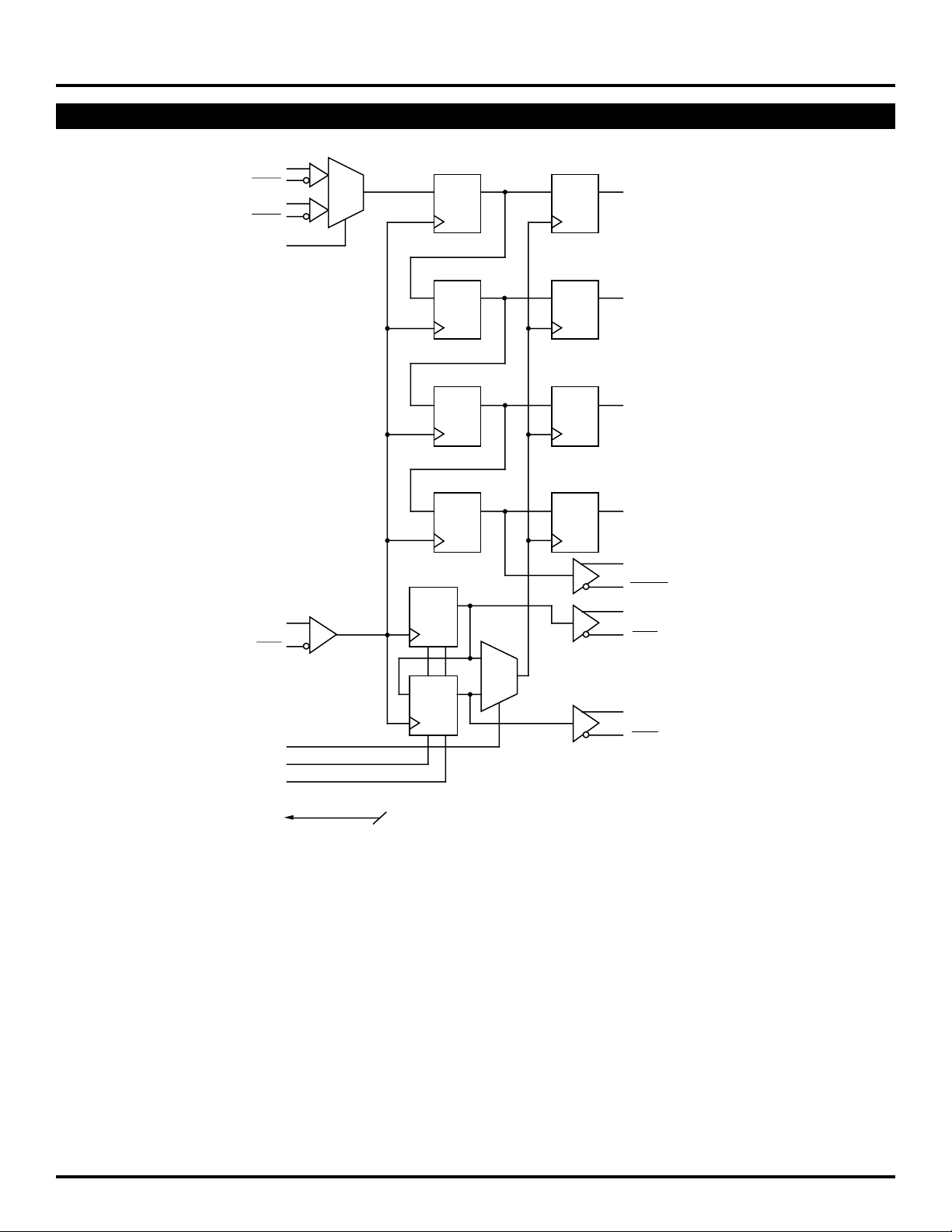
The SY10/100E445 are integrated 4-bit serial-to-parallel
data converters. The devices are designed to operate for
NRZ data rates of up to 2.5Gb/s. The chip generates a
divide-by-4 and a divide-by-8 clock for both 4-bit conversion
and a two-chip 8-bit conversion function. The conversion
sequence was chosen to convert the first serial bit to Q
the second to Q1, etc.
Two selectable serial inputs provide a loopback capability
for testing purposes when the device is used in conjunction
with the E446 parallel-to-serial converter.
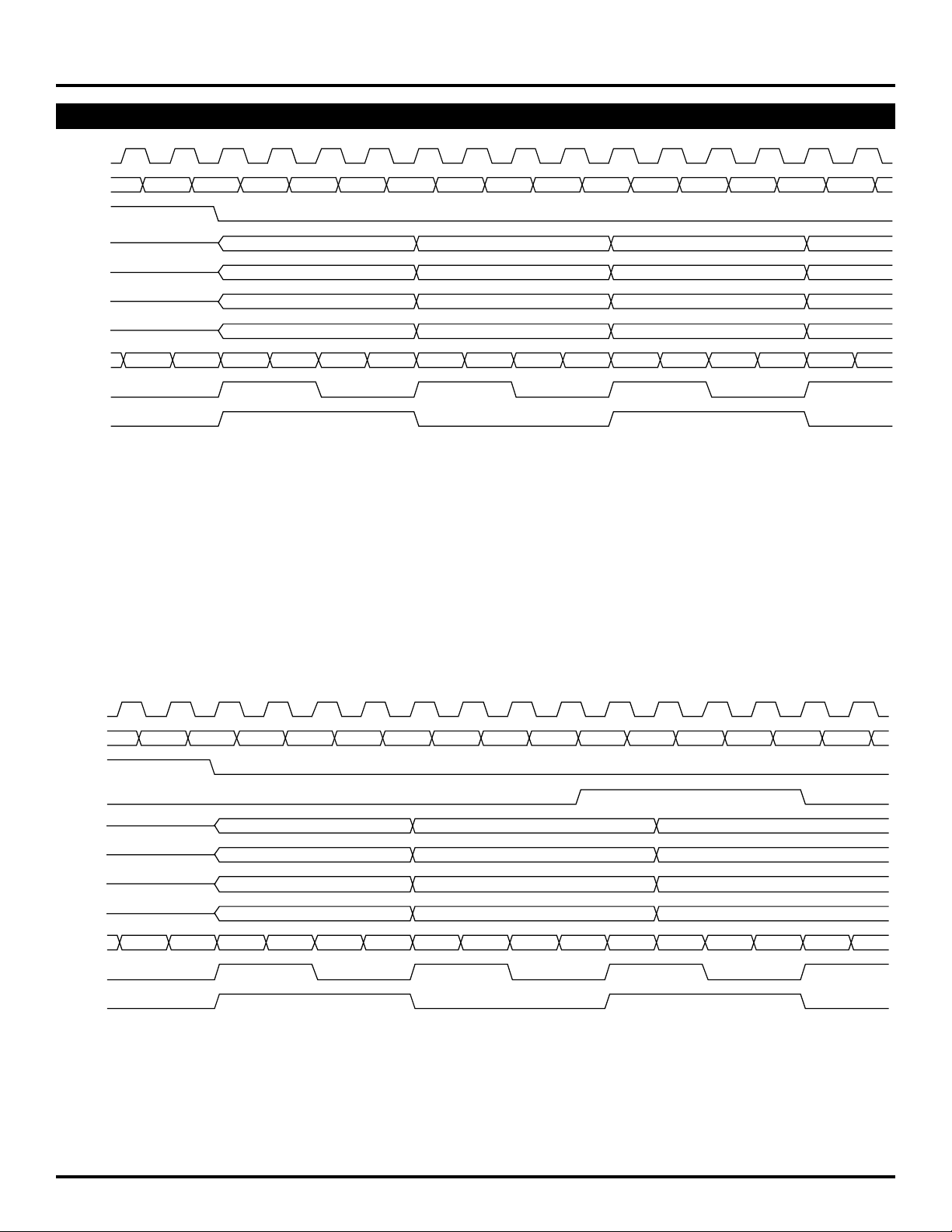
The start bit for conversion can be moved using the
SYNC input. A single pulse, applied asynchronously for at
least two input clock cycles, shifts the start bit for conversion
from Qn to Qn-1 by one bit. For each additional shift required,
an additional pulse must be applied to the SYNC input.
Asserting the SYNC input will force the internal clock dividers
to "swallow" a clock pulse, effectively shifting a bit from the
Qn to the Qn-1 output (see Timing Diagram B).
The MODE input is used to select the conversion mode
of the device. With the MODE input LOW (or open) the
device will function as a 4-bit converter. When the mode
input is driven HIGH, the data on the output will change on
every eighth clock cycle, thus allowing for an 8-bit conversion
scheme using two E445s. When cascaded in an 8-bit
conversion scheme, the devices will not operate at the
2.5Gb/s data rate of a single device. Refer to the applications
section of this data sheet for more information on cascading
the E445.
For lower data rate applications, a VBB reference voltage
is supplied for single-ended inputs. When operating at clock
rates above 500MHz, differential input signals are
recommended. For single-ended inputs, the VBB pin is tied
to the inverting differential input and bypassed via a 0.01µF
capacitor. The VBB provides the switching reference for the
input differential amplifier. The VBB can also be used to AC
couple an input signal.
0,
Rev.: D Amendment: /0
1
Issue Date: October, 1998
Page 2
Micrel
BLOCK DIAGRAM
SY10E445
SY100E445
SINB
SINB
SINA
SINA
SEL
CLK
CLK
0
1
DQ
D
DQ
DQ
DQ
DQ
DQ
DQ
DQ
Q
3
Q
2
Q
1
Q
0
SOUT
SOUT
÷4
R
CL/4
CL/4
0
MODE
RESET
SYNC
VBB
R
÷2
1
CL/8
CL/8
2
Page 3
Micrel
TRUTH TABLES
LOGIC DIAGRAM
SY10E445
SY100E445
Mode Conversion
L 4-Bit
H 8-Bit
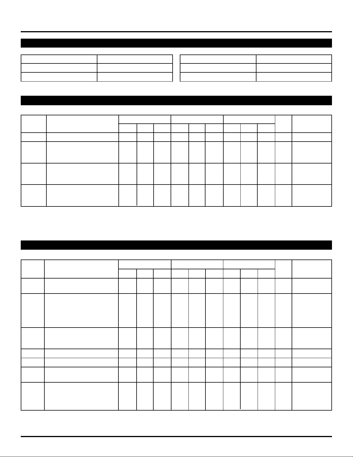
DC CHARACTERISTICS
LOGIC DIAGRAM
SEL Serial Input
HA
LB
VEE = VEE (Min.) to VEE (Max.); VCC = VCCO = GND
TA = 0°CTA = +25°CTA = +85°C
Symbol Parameter Min. Typ. Max. Min. Typ. Max. Min. Typ. Max. Unit Condition
IIH Input HIGH Current ——150 ——150 ——150 µA —
OH Output HIGH Voltage V
V
(SOUT only) 10E –1020 —–790 –980 —–760 –910 —–670 1
(SOUT only) 100E –1025 —–830 –1025 —–830 –1025 —–830 1
V
BB Output Reference Voltage V
10E –1.38 —–1.27 –1.35 —–1.25 –1.31 —–1.19
100E –1.38 —–1.26 –1.38 —–1.26 –1.38 —–1.26
EE Power Supply Current mA —
I
10E — 154 185 — 154 185 — 154 185
100E — 154 185 — 154 185 — 177 212
NOTE:
1. The maximum VOH limit was relaxed from standard ECL due to the high frequency output design. All other outputs are specified with the standard 10E
and 100E VOH levels.
AC CHARACTERISTICS
LOGIC DIAGRAM
VEE = VEE (Min.) to VEE (Max.); VCC = VCCO = GND
TA = 0°CTA = +25°CTA = +85°C
Symbol Parameter Min. Typ. Max. Min. Typ. Max. Min. Typ. Max. Unit Condition
MAX Max. Conversion Frequency 2.0 ——2.0 ——2.0 ——Gb/s 1
f
2.5 ——2.5 ——2.5 ——NRZ 2
PLH Propagation Delay to Output ps —
t
tPHL CLK to Q 1500 1800 2100 1500 1800 2100 1500 1800 2100
CLK to SOUT 800 975 1150 800 975 1150 800 975 1150
CLK to CL/4 1100 1325 1550 1100 1325 1550 1100 1325 1550
CLK to CL/8 1100 1325 1550 1100 1325 1550 1100 1325 1550
S Set-up Time ps —
t
SINA, SINB –100 –250 —–100 –250 —–100 –250 —
SEL 0 –200 — 0 –200 — 0 –200 —
tH Hold Time, SINA, SINB, SEL 450 300 — 450 300 — 450 300 — ps —
tRR Reset Recovery Time 500 300 — 500 300 — 500 300 — ps —
t
PW Minimum Pulse Width 400 ——400 ——400 ——ps —
CLK, MR
r Rise/Fall Times ps —
t
tf 20% to 80%
SOUT 100 225 350 100 225 350 100 225 350
Other 200 425 650 200 425 650 200 425 550
NOTES:
1. Guaranteed for input clock amplitudes of 150mV to 800mV.
2. Guaranteed for input clock amplitudes of 150mV to 400mV.
3
Page 4
Micrel
k
k
k
LOGIC DIAGRAMAPPLICATIONS INFORMATION
SY10E445
SY100E445
The SY10/100E are integrated 1:4 serial-to-parallel
converters. The chips are designed to work with the
E446 devices to provide both transmission and receiving
of a high-speed serial data path. The E445, under special
input conditions, can convert up to a 2.5Gb/s NRZ data
stream into 4-bit parallel data. The device also provides
a divide-by-four clock output to be used to synchronize
the parallel data with the rest of the system.
The E445 features multiplexed dual serial inputs to
provide test loop capability when used in conjunction
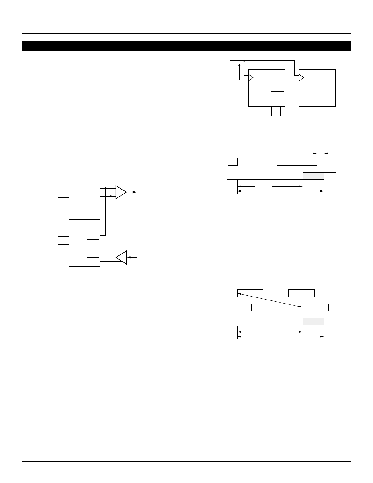
with the E446. Figure 1 illustrates the loop test
architecture. The architecture allows for the electrical
testing of the link without requiring actual transmission
over the serial data path medium. The SINA serial input
of the E445 has an extra buffer delay and, thus, should
be used as the loop back serial input.
Parallel
Data
Parallel
Data
SOUT
SOUT
SINA
SINA
SINB
SINB
Figure 1. Loop Test Architecture
To Serial
Medium
From Serial
Medium
Cloc
Cloc
E445a
3
Q
800ps
2Q1
SOUT
SOUT
Q
1050ps
0
4
Serial Input
Data
Cloc
Tpd CLK
to SOUT
Figure 2. Cascaded 1:8 Converter Architecture
SIN
SIN
Q
Q7Q6Q5Q
Parallel Output Data
E445b
SIN
SIN
3
2Q1
Q
Q
Q3Q2Q1Q
100ps
Q
0
0
clock-to-serial-out would potentially cause a serial bit to
be swallowed (Figure 3). With a minimum delay of 800ps
on this output, the clock for the lower order E445 cannot
be delayed more than 800ps relative to the clock of the
first E445 without potentially missing a bit of information.
Because the set-up time on the serial input pin is
negative, coincident excursions on the data and clock
inputs of the E445 will result in correct operation.
The E445 features a differential serial output and a
divide-by-8 clock output to facilitate the cascading of two
devices to build a 1:8 demultiplexer. Figure 2 illustrates
the architecture of a 1:8 demultiplexer using two E445s.
The timing diagram for this configuration can be found
on the following page. Notice the serial outputs (SOUT)
of the lower order converter feed the serial inputs of the
higher order device. This feedthrough of the serial inputs
bounds the upper end of the frequency of operation. The
clock-to-serial output propagation delay, plus the set-up
time of the serial input pins, must fit into a single clock
period for the cascade architecture to function properly.
Using the worst case values for these two parameters
from the data sheet, tPD CLK to SOUT = 1150ps or a
clock frequency of 950MHz.
The clock frequency is significantly lower than that of
a single converter. To increase this frequency, some
games can be played with the clock input of the higher
order E445. By delaying the clock feeding the second
E445 relative to the clock of the first E445, the frequency
of operation can be increased. The delay between the
two clocks can be increased until the minimum delay of
Clock a
Clock b
Tpd CLK
to SOUT
Figure 3. Cascade Frequency Limitation
800ps
1050ps
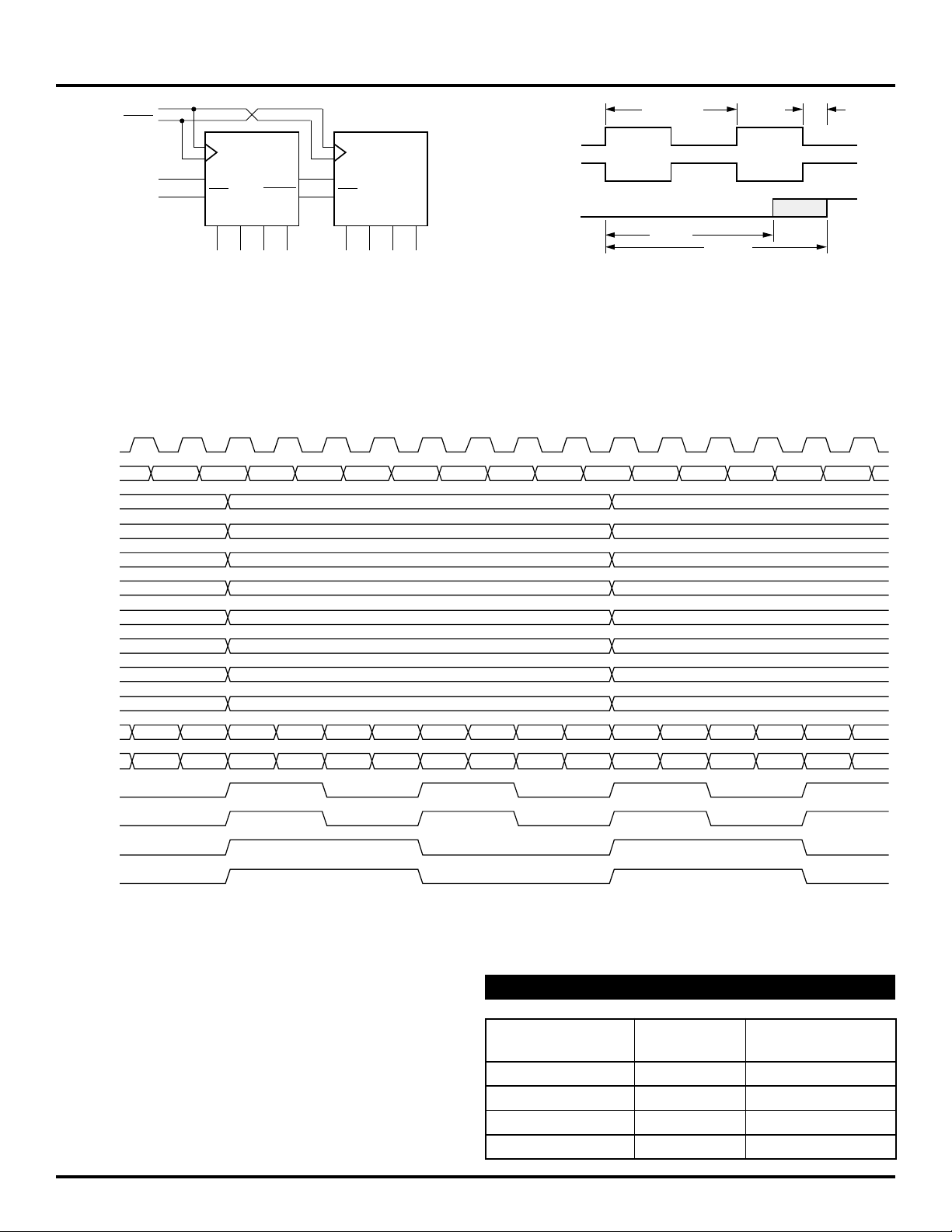
Perhaps the easiest way to delay the second clock
relative to the first is to take advantage of the differential
clock inputs of the E445. By connecting the clock for the
second E445 to the complimentary clock input pin, the
device will clock a half a clock period after the first E445
(Figure 4). Utilizing this simple technique will raise the
potential conversion frequency up to 1.5GHz. The divideby-eight clock of the second E445 should be used to
synchronize the parallel data to the rest of the system as
the parallel data of the two E445s will no longer be
synchronized. This skew problem between the outputs
can be worked around as the parallel information will be
static for eight more clock pulses.
4
Page 5
Micrel
LOGIC DIAGRAMTIMING DIAGRAMS
CLK
SY10E445
SY100E445
SIN
RESET
Q0
Q1
Q2
Q3
SOUT
CL/8
CL/4
Dn–4Dn–3Dn–2Dn–1 Dn Dn+1 Dn+2 Dn+3
Dn–4
Dn–3
Dn–2
Dn–1
Dn–4Dn–3Dn–2Dn–1 Dn Dn+1 Dn+2 Dn+3
Timing Diagram A. 1:4 Serial to Parallel Conversion
Dn
Dn+1
Dn+2
Dn+3
CLK
SIN
RESET
SYNC
Q
Q
Q
Q
SOUT
CL/4
CL/8
Dn–4
0
1
2
3
Dn–3Dn–2Dn–1 Dn Dn+1 Dn+2 Dn+3 Dn+4
Dn–4
Dn–3
Dn–2
Dn–1
Dn–4Dn–3Dn–2Dn–1 Dn Dn+1 Dn+2 Dn+3 Dn+4
Dn+1
Dn+2
Dn+3
Dn+4
Timing Diagram B. 1:4 Serial to Parallel Conversion with SYNC Pulse
5
Page 6
Micrel
k
k
SY10E445
SY100E445
Serial Input
CLK
SINa
Q
0
Q
1
Cloc
Cloc
Data
E445a
SIN
SIN
Q
Q7Q6Q5Q
SOUT
SOUT
Q
3
2Q1
Q
0
4
Parallel Output Data
Dn–4
(1.5GHz)
E445b
SIN
Clock a
Clock b
SIN
3
2Q1
Q
Q
Q3Q2Q1Q
Q
0
0
Tpd CLK
to SOUT
Figure 4. Extended Frequency 1:8 Demultiplexer
Dn–3Dn–2Dn–1 Dn Dn+1 Dn+2 Dn+3 Dn+4
667ps
800ps
100ps
1050ps
Dn–4
Dn–3
Q
Q
Q4 (Q0 a)
Q5 (Q1 a)
Q6 (Q2 a)
Q7 (Q3 a)
SOUTa
SOUTb
CL/4a
CL/4b
CL/8a
CL/8b
2
3
Dn–4Dn–3Dn–2Dn–1 Dn Dn+1 Dn+2 Dn+3
Dn–4Dn–3Dn–2Dn–1Dn Dn+1
Dn–2
Dn–1
Dn
Dn+1
Dn+2
Dn+3
Timing Diagram
PRODUCT ORDERING CODE
Ordering Package Operating
Code Type Range
SY10E445JC J28-1 Commercial
SY10E445JCTR J28-1 Commercial
SY100E445JC J28-1 Commercial
SY100E445JCTR J28-1 Commercial
6
Page 7
Micrel
28 LEAD PLCC (J28-1)
SY10E445
SY100E445
Rev. 03
7
Page 8

Micrel
SY10E445
SY100E445
MICREL-SYNERGY 3250 SCOTT BOULEVARD SANTA CLARA CA 95054 USA
TEL + 1 (408) 980-9191 FAX + 1 (408) 914-7878 WEB http://www.micrel.com
This information is believed to be accurate and reliable, however no responsibility is assumed by Micrel for its use nor for any infringement of patents or
other rights of third parties resulting from its use. No license is granted by implication or otherwise under any patent or patent right of Micrel Inc.
© 2000 Micrel Incorporated
8
 Loading...