

Page 1
QUAD DIFFERENTIAL
AND/NAND
SY10E404
SY100E404
FEATURES
■ Differential D and Q
■ Extended 100E V
EE range of –4.2V to –5.5V
■ 700ps max. propagation delay
■ High frequency outputs
■ Internal 75KΩ input pull-down resistors
■ Fully compatible with Motorola 10E/100E404
■ Available in 28-pin PLCC package
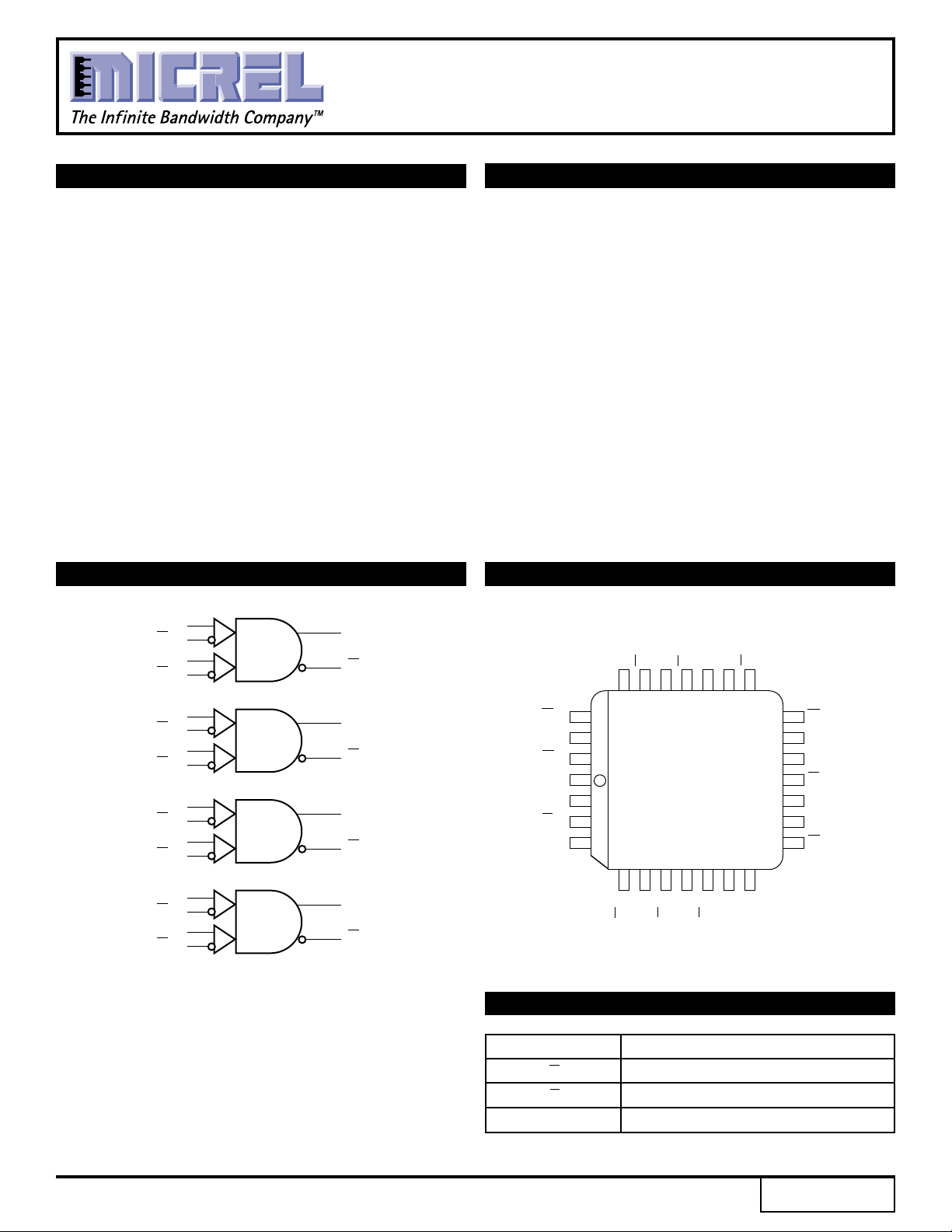
BLOCK DIAGRAM
D
0a
D
0a
D
0b
D
0b
D
1a
D
1a
D
1b
D
1b
D
2a
D
2a
D
2b
D
2b
Q
0
Q
0
Q
1
Q
1
Q
2
Q
2
DESCRIPTION
The SY10/100E404 are 4-bit differential AND/NAND
devices. The differential operation of these devices make
them ideal for pulse shaping applications where duty cycle
skew is critical. Special design techniques were
incorporated to minimize the skew between the upper
and lower level gate inputs.
Because a negative 2-input NAND function is
equivalent to a 2-input OR function, the differential inputs
and outputs of the devices also allow for their use as
fully differential 2-input OR/NOR functions.
The output RISE/FALL times of these devices are
significantly faster than most other standard ECLinPS
devices, resulting in an increased bandwidth.
The differential inputs have clamp structures which
will force the Q output of a gate in an open input condition
to go to a LOW state. Thus, inputs of unused gates can
be left open and will not affect the operation of the rest
of the device.
PIN CONFIGURATION
D3b
D3a
D2b
D2b
D2a
VEE
D2a
D1b
D1b
D3a
25
24 23 22 21 20 19
26
27
28
1
2
3
4
TOP VIEW
PLCC
J28-1
567891011
Q3
D3b
VCCO
Q3
18
Q2
17
Q2
16
VCC
15
Q1
14
Q1
13
Q0
12
Q0
D
3a
D
3a
D
3b
D
3b
Q
3
Q
3
D1a
D0b
D1a
D0a
D0b
D0a
VCCO
PIN NAMES
Pin Function
D[0:4], D[0:4] Differential Data Inputs
Q[0:4], Q[0:4] Differential Data Outputs
CCO VCC to Output
V
Rev.: D Amendment: /1
1
Issue Date: February, 1998
Page 2
SY10E404
Micrel
SY100E404
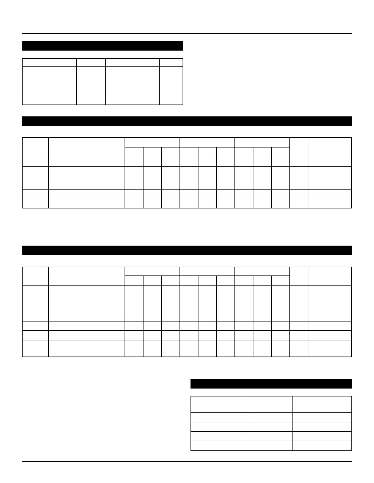
TRUTH TABLE
Da Db Q Da Db Q
LL L L LL
LH L L HH
HL L H LH
HH H H HH
DC ELECTRICAL CHARACTERISTICS
VEE = VEE (Min.) to VEE (Max.); VCC = VCCO = GND
TA = 0°CTA = +25°CTA = +85°C
Symbol Parameter Min. Typ. Max. Min. Typ. Max. Min. Typ. Max. Unit Condition
IIH Input HIGH Current — — 150 — — 150 — — 150 µA—
EE Power Supply Current mA —
I
10E — 106 127 — 106 127 — 106 127
100E — 106 127 — 106 127 — 122 146
VPP (DC) Input Sensitivity 50 — — 50 — — 50 — — mV 1
V
CMR Common Mode Range –1.5 — 0 –1.5 — 0 –1.5 — 0 V 2
NOTES:
1. Differential input voltage required to obtain a full ECL swing on the outputs.
2. VCMR is referenced to the most positive side of the differential input signal. Normal operation is obtained when the input signals are within the VCMR range
and the input swing is greater than VPP (min.) and <1V.
AC ELECTRICAL CHARACTERISTICS
VEE = VEE (Min.) to VEE (Max.); VCC = VCCO = GND
TA = 0°CTA = +25°CTA = +85°C
Symbol Parameter Min. Typ. Max. Min. Typ. Max. Min. Typ. Max. Unit Condition
PLH Propagation Delay to Output ps —
t
tPHL Da (Diff) 350 475 650 350 475 650 350 475 650
Da (SE) 300 475 700 300 475 700 300 475 700
Db (Diff) 375 500 675 375 500 675 375 500 675
Db (SE) 325 500 725 325 500 725 325 500 725
tskew Within-Device Skew — 50 — — 50 — — 50 — ps 1
VPP(AC) Minimum Input Swing 150 — — 150 — — 150 — — mV 2
r Rise/Fall Time 150 — 400 150 — 400 150 — 400 ps —
t
tf 20–80%
NOTES:
1. Within-device skew is defined as identical transitions on similar paths
through a device.
2. Minimum input swing for which AC parameters are guaranteed.
PRODUCT ORDERING CODE
Ordering Package Operating
Code Type Range
SY10E404JC J28-1 Commercial
SY10E404JCTR J28-1 Commercial
SY100E404JC J28-1 Commercial
SY100E404JCTR J28-1 Commercial
2
Page 3
Micrel
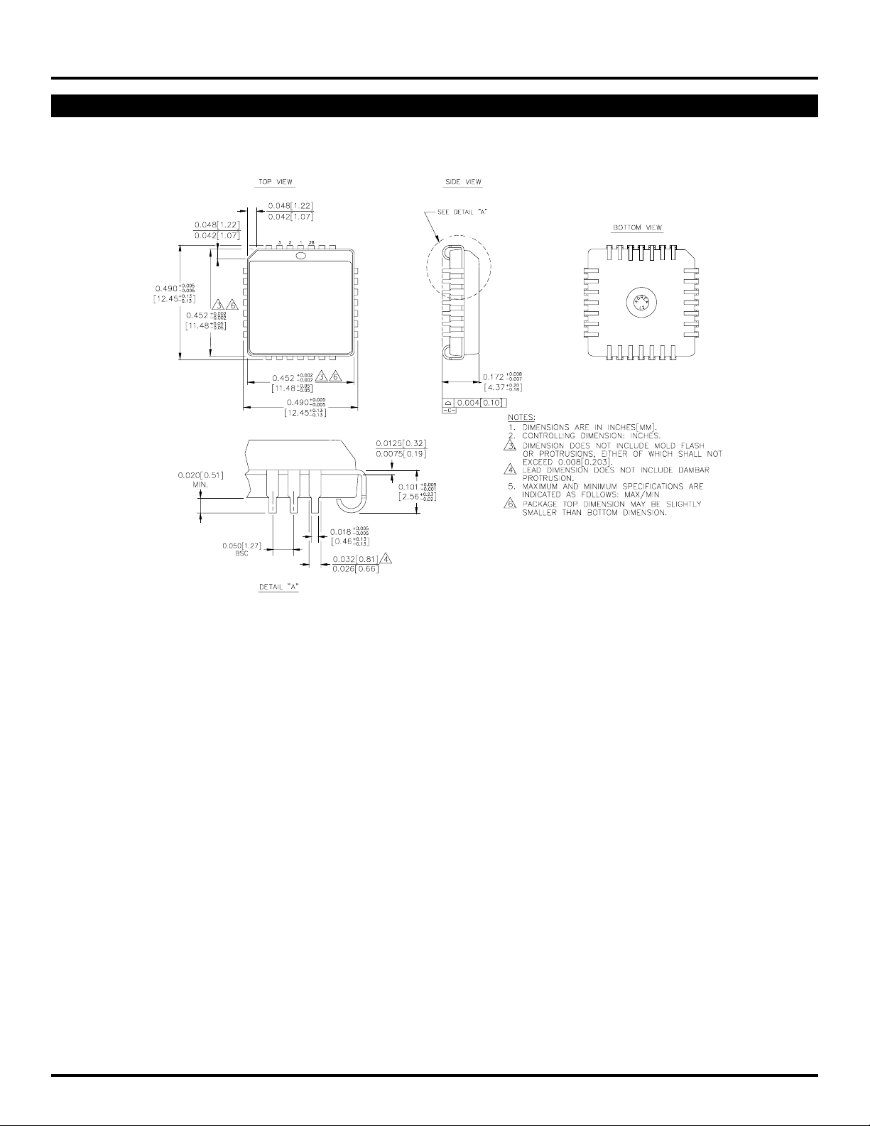
28 LEAD PLCC (J28-1)
SY10E404
SY100E404
Rev. 03
3
Page 4

Micrel
SY10E404
SY100E404
MICREL-SYNERGY 3250 SCOTT BOULEVARD SANTA CLARA CA 95054 USA
TEL + 1 (408) 980-9191 FAX + 1 (408) 914-7878 WEB http://www.micrel.com
This information is believed to be accurate and reliable, however no responsibility is assumed by Micrel for its use nor for any infringement of patents or
other rights of third parties resulting from its use. No license is granted by implication or otherwise under any patent or patent right of Micrel Inc.
© 2000 Micrel Incorporated
4
 Loading...