

Page 1
3-BIT REGISTERED
BUS TRANSCEIVER
SY10E336
SY100E336
FEATURES
■ 25Ω cutoff bus output
■ Extended 100E VEE range of –4.2V to –5.5V
■ 50Ω receiver output
■ Transmit and receive registers
■ 1500ps max. clock to bus
■ 1000ps max. clock to Q
■ Internal edge slow-down capacitors on bus outputs
■ Additional package ground pins
■ Fully compatible with industry standard 10KH,
100K ECL levels
■ Internal 75KΩ input pulldown resistors
■ Fully compatible with Motorola MC10E/100E336
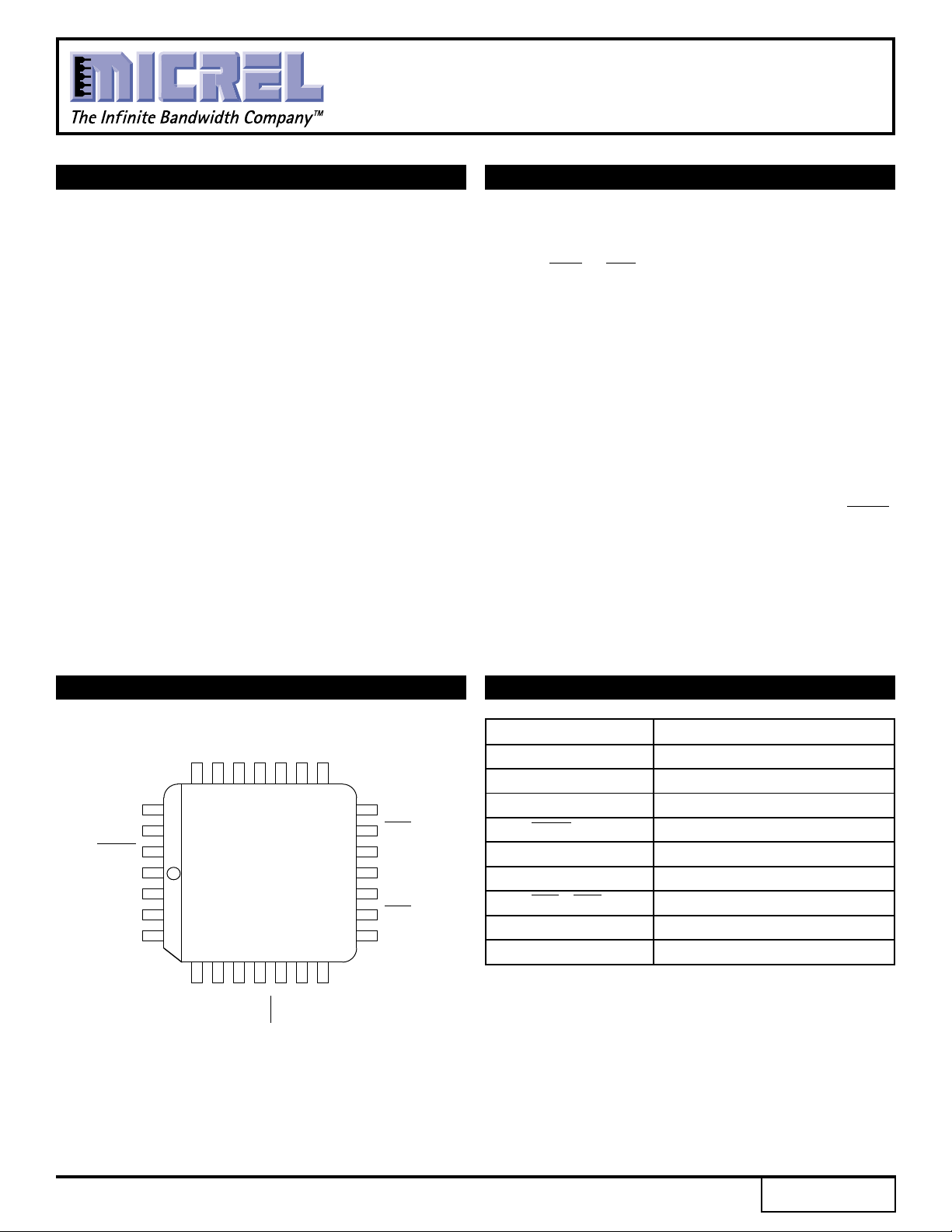
■ Available in 28-pin PLCC package
DESCRIPTION
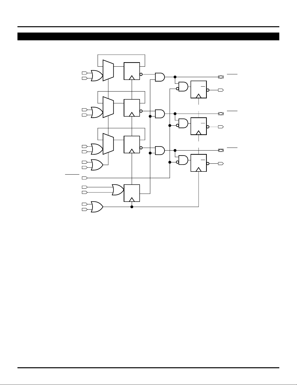
The SY10/100E336 offer three bus transceivers with
both transmit and receive registers and are designed for
use in new, high-performance ECL systems. The bus
outputs (BUS0 - BUS2) are designed to drive a 25Ω bus.
The receive outputs (Q0 – Q2) are specified for 50Ω. The
bus outputs feature a normal logic HIGH level (VOH) and a
cutoff LOW level when at a logic LOW. At cutoff, the outputs
go to –2.0V and the output emitter-follower is “off”,
presenting a high impedance to the bus. The bus outputs
have edge slow-down capacitors.
The Transmit Enable pins (TEN) determine whether
current data is held in the transmit register or new data is
loaded from the A/B inputs. A logic LOW on both of the bus
enable inputs (BUSEN), when clocked through the register,
disables the bus outputs to –2.0V.
The receiver section clocks bus data into the receive
registers after gating with the Receive Enable (RXEN)
input.
All registers are clocked by rising edge of CLK1 or CLK2
(or both).
Additional grounding is provided through the ground
pins (GND) which should be connected to 0V. The GND
pins are not electrically connected to the chip.
PIN CONFIGURATION
1
2
2
B
TEN
TEN
25 24 23 22 21 20 19
EE
A
26
1
27
2
28
1
2
1
3
2
4
0
TOP VIEW
PLCC
J28-1
5 6 7 8 9 10 11
1
0
B
A1B
BUSEN
BUSEN
RXEN
V
CLK
CLK
2
A
CCO
V
NC
0
BUS
CCO
V
GND
PIN NAMES
2
Q
18
GND
17
BUS
2
16
V
CC
15
14
13
12
0
Q
1
Q
V
CCO
BUS
GND
1
Pin Function
A0–A2 Data Inputs A
B0–B2 Data Inputs B
TEN1, 2 Transmit Enable Inputs
RXEN Receive Enable Input
BUSEN1, 2 Bus Enable Inputs
CLK1, 2 Clock Inputs
BUS0–BUS2 25Ω Cutoff Bus Outputs
Q0–Q2 Receive Data Outputs
CCO VCC to Output
V
Rev.: C Amendment: /2
1
Issue Date: February, 1998
Page 2
Micrel
BLOCK DIAGRAM
SY10E336
SY100E336
A0
B0
A1
B1
A2
B2
TEN1
TEN2
RXEN
BUSEN1
BUSEN2
CLK1
CLK2
0
1
0
1
0
1
DQ
DQ
DQ
25 CUTOFF
D
Q
25 CUTOFF
D
Q
25 CUTOFF
D
Q
50
50
50
BUS0
0
Q
BUS1
Q1
BUS2
Q2
D
Q
2
Page 3
Micrel
SY100E336
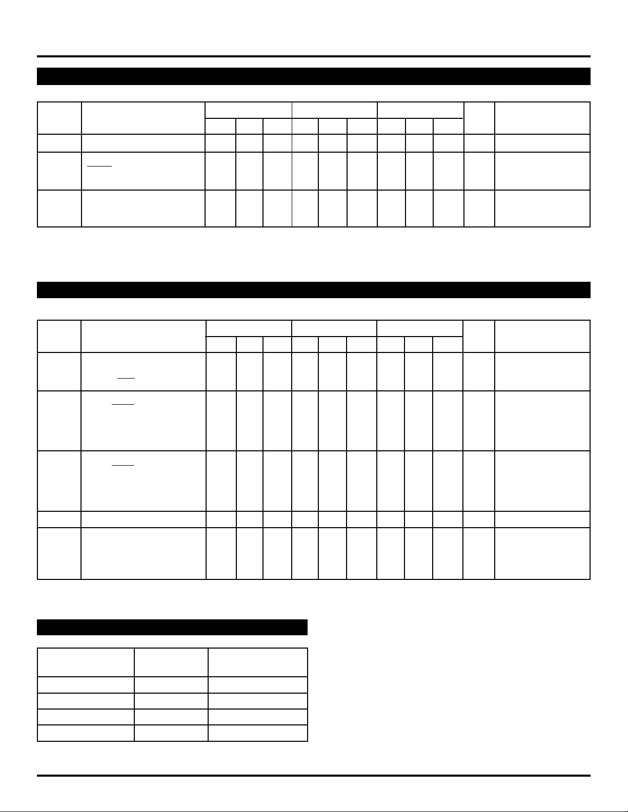
DC ELECTRICAL CHARACTERISTICS
VEE = VEE (Min.) to VEE (Max.); VCC = VCCO = GND
TA = 0°CTA = +25°CTA = +85°C
Symbol Parameter Min. Typ. Max. Min. Typ. Max. Min. Typ. Max. Unit Condition
VCUT Cut-off Output Voltage –2.10 —–2.03 –2.10 —–2.03 –2.10 —–2.03 V 1
IH Input HIGH Current µA —
I
RXEN ——225 ——225 ——225
All Other Inputs ——150 ——150 ——150
EE Power Supply Current mA —
I
10E — 125 150 — 125 150 — 125 150
100E — 125 150 — 125 150 — 144 173
NOTE:
1. Measured with VTT = –2.10V.
AC ELECTRICAL CHARACTERISTICS
VEE = VEE (Min.) to VEE (Max.); VCC = VCCO = GND
TA = 0°CTA = +25°CTA = +85°C
Symbol Parameter Min. Typ. Max. Min. Typ. Max. Min. Typ. Max. Unit Condition
PLH Propagation Delay to Output ps —
t
tPHL CLK to Q 500 700 1000 500 700 1000 500 700 1000
CLK to BUS 825 1250 1800 825 1250 1800 825 1250 1800
S Set-up Time ps —
t
BUS, RXEN 150 –150 — 150 –150 — 150 –150 —
BUSEN 100 –200 — 100 –200 — 100 –200 —
A, B Data 300 –50 — 300 –50 — 300 –50 —
TEN 450 150 — 450 150 — 450 150 —
H Hold Time ps —
t
BUS, RXEN 450 150 — 450 150 — 450 150 —
BUSEN 500 200 — 500 200 — 500 200 —
A, B Data 350 50 — 350 50 — 350 50 —
TEN 200 –150 — 200 –150 — 200 –150 —
tPW Minimum Pulse Width, CLK 400 ——400 ——400 ——ps —
r Rise/Fall Time ps —
t
tf 20% to 80% (Qn) 300 450 700 300 450 700 300 450 700
20% to 80% (BUSn Rise) 500 800 1000 500 800 1000 500 800 1000
20% to 80% (BUSn Fall) 300 500 800 300 500 800 300 500 800
SY10E336
PRODUCT ORDERING CODE
Ordering Package Operating
Code Type Range
SY10E336JC J28-1 Commercial
SY10E336JCTR J28-1 Commercial
SY100E336JC J28-1 Commercial
SY100E336JCTR J28-1 Commercial
3
Page 4
Micrel
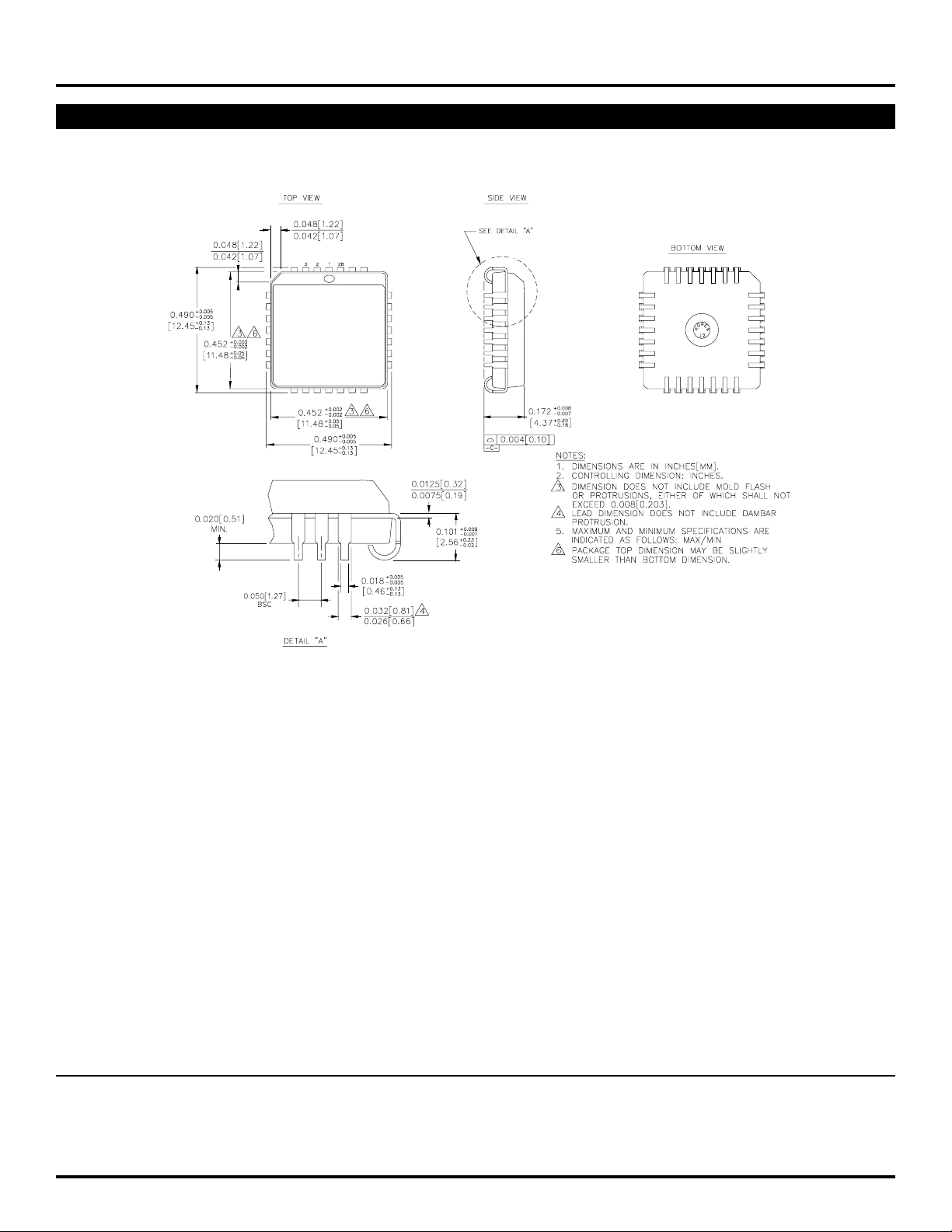
28 LEAD PLCC (J28-1)
SY10E336
SY100E336
Rev. 03
MICREL-SYNERGY 3250 SCOTT BOULEVARD SANTA CLARA CA 95054 USA
TEL + 1 (408) 980-9191 FAX + 1 (408) 914-7878 WEB http://www.micrel.com
This information is believed to be accurate and reliable, however no responsibility is assumed by Micrel for its use nor for any infringement of patents or
other rights of third parties resulting from its use. No license is granted by implication or otherwise under any patent or patent right of Micrel Inc.
© 2000 Micrel Incorporated
4
 Loading...