

Page 1
9-BIT SHIFT
REGISTER
SY10E142
SY100E142
FEATURES
■ 700MHz min. shift frequency
■ Extended 100E V
EE range of –4.2V to –5.5V
■ 9 bits wide for byte-parity applications
■ Asynchronous Master Reset
■ Dual clocks
■ Fully compatible with industry standard 10KH,
100K ECL levels
■ Internal 75KΩ input pulldown resistors
■ Fully compatible with Motorola MC10E/100E142
■ Available in 28-pin PLCC package
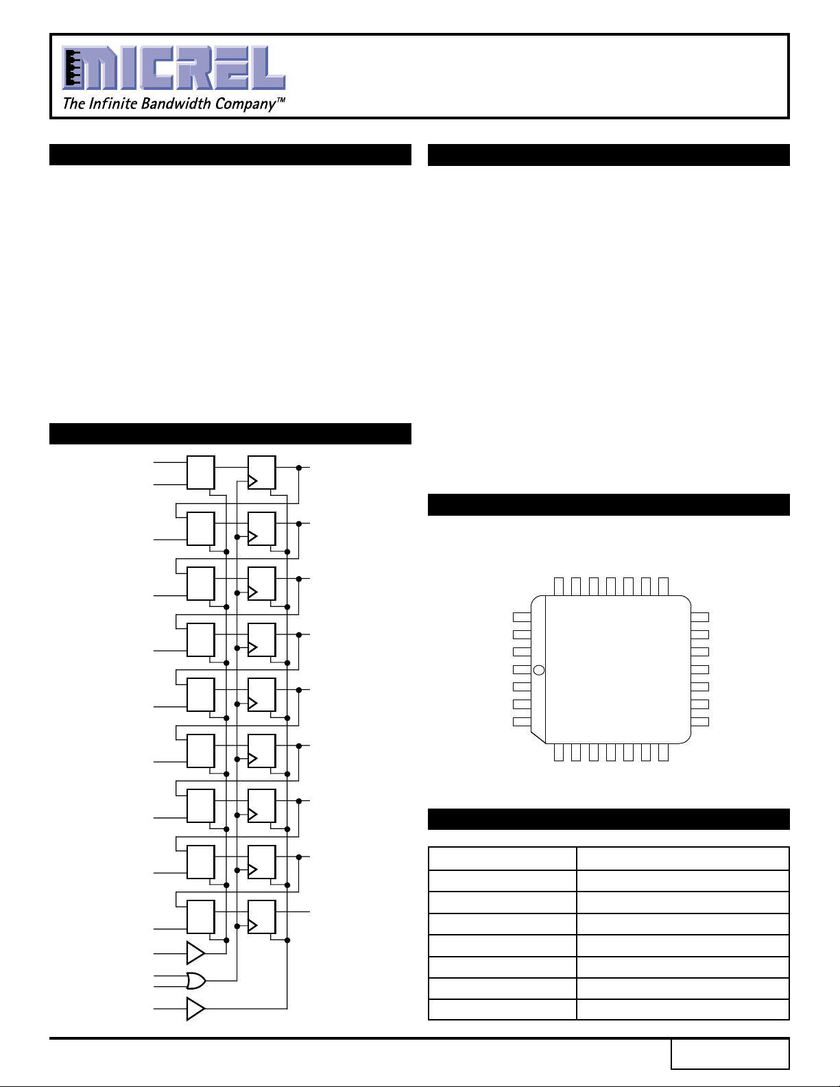
BLOCK DIAGRAM
S-IN
D
D
0
1
1 DQ
0
1
0
DQ
Q0
Q1
DESCRIPTION
The SY10/100E142 are high-speed 9-bit shift registers
designed for use in new, high-performance ECL systems.
The E142 can accept serial or parallel data to be shifted out
in one direction as both serial and parallel outputs. The
nine inputs, D
0-D8, accept parallel input data, while S-IN
accepts serial input data.
The SEL (Select) control pin serves to determine the
mode of operation, either SHIFT or LOAD. The shift direction
is from bit 0 to bit 8. The input data has to meet the set-up
time before being clocked into the nine input registers on
the rising edge of CLK1 or CLK2. Shifting is also performed
on the rising edge of either CLK1 or CLK2. The MR (Master
Reset) control signal asynchronously resets all nine
registers to a logic LOW when a logic HIGH is applied to
MR.
The E142 is designed for applications such as diagnostic
scan registers, parallel-to-serial conversions and is also
suitable for byte-wide parity.
PIN CONFIGURATION
D2
D3
D4
D5
D6
D7
D8
SEL
CLK1
CLK2
MR
SEL
1
0
1
0
1
0
1
0
1
0
1
0
1
0
DQ
DQ
DQ
DQ
DQ
DQ
DQ
Q2
Q3
Q4
Q5
Q6
Q7
Q8
MR
CLK
CLK
V
S-IN
EE
D
D
26
1
27
2
28
1
2
0
3
1
4
PIN NAMES
Pin Function
D0-D8 Parallel Data Inputs
S-IN Serial Data Input
SEL Mode Select Input
D
25 24 23 22 21 20 19
PLCC
TOP VIEW
J28-1
567891011
3
4
2
D
D
D
D
CCO
V
V
D
Q
18
Q
7
17
Q
6
16
V
CC
Q
V
Q
Q
5
CCO
4
3
15
14
13
12
1
0
2
Q
Q
Q
8
5
CCO
6D7
8
CLK1, CLK2 Clock Inputs
MR Master Reset
Q0-Q8 Data Outputs
CCO VCC to Output
V
Rev.: C Amendment: /1
1
Issue Date: February, 1998
Page 2
SY10E142
Micrel
SY100E142
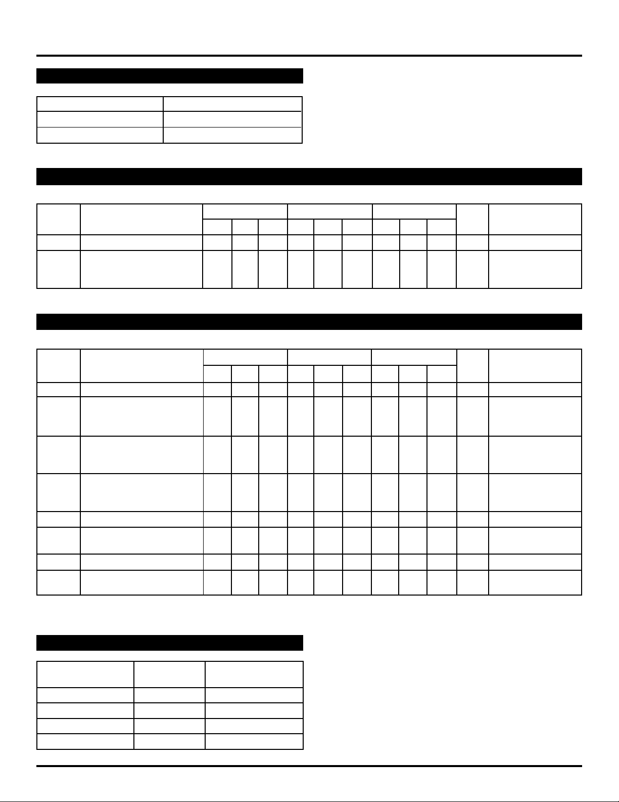
TRUTH TABLE
SEL MODE
L LOAD
H SHIFT
DC ELECTRICAL CHARACTERISTICS
VEE = VEE (Min.) to VEE (Max.); VCC = VCCO = GND
TA = 0°CTA = +25°CTA = +85°C
Symbol Parameter Min. Typ. Max. Min. Typ. Max. Min. Typ. Max. Unit Condition
IIH Input HIGH Current — — 150 — — 150 — — 150 µA—
I
EE Power Supply Current mA —
10E — 120 145 — 120 145 — 120 145
100E — 120 145 — 120 145 — 138 165
AC ELECTRICAL CHARACTERISTICS
VEE = VEE (Min.) to VEE (Max.); VCC = VCCO = GND
TA = 0°CTA = +25°CTA = +85°C
Symbol Parameter Min. Typ. Max. Min. Typ. Max. Min. Typ. Max. Unit Condition
fSHIFT Max. Shift Frequency 700 900 — 700 900 — 700 900 — MHz —
tPLH Propagation Delay to Output ps —
tPHL CLK 600 800 1000 600 800 1000 600 800 1000
MR 600 800 1000 600 800 1000 600 800 1000
S Set-up Time ps —
t
D 50 –100 — 50 –100 — 50 –100 —
SEL 300 150 — 300 150 — 300 150 —
H Hold Time ps —
t
D 300 100 — 300 100 — 300 100 —
SEL 75 –150 — 75 –150 — 75 –150 —
tRR Reset Recovery Time 900 700 — 900 700 — 900 700 — ps —
PW Minimum Pulse Width 400 — — 400 — — 400 — — ps —
t
CLK, MR
tskew Within-Device Skew — 75 — — 75 — — 75 — ps 1
t
r Rise/Fall Time 300 525 800 300 525 800 300 525 800 ps —
tf 20% to 80%
NOTE:
1. Within-device skew is defined as identical transitions on similar paths through a device.
PRODUCT ORDERING CODE
Ordering Package Operating
Code Type Range
SY10E142JC J28-1 Commercial
SY10E142JCTR J28-1 Commercial
SY100E142JC J28-1 Commercial
SY100E142JCTR J28-1 Commercial
2
Page 3
Micrel
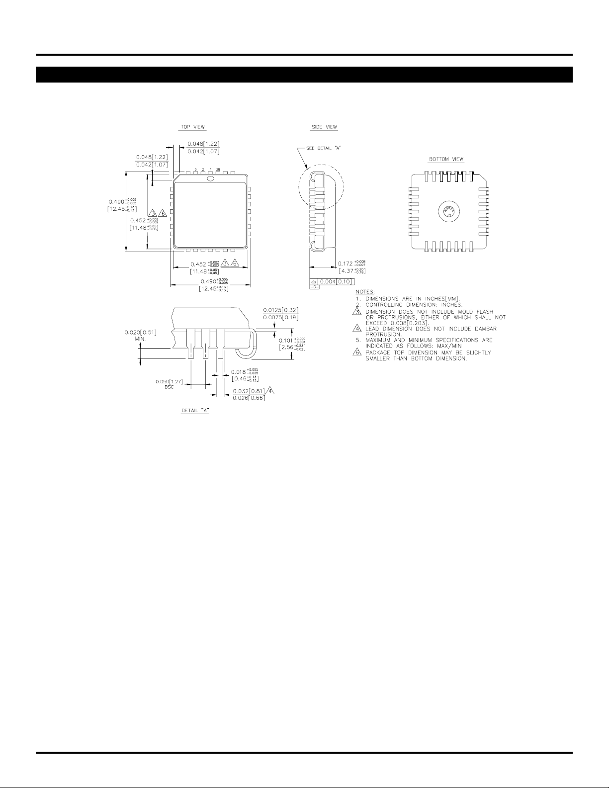
28 LEAD PLCC (J28-1)
SY10E142
SY100E142
Rev. 03
3
Page 4

Micrel
SY10E142
SY100E142
MICREL-SYNERGY 3250 SCOTT BOULEVARD SANTA CLARA CA 95054 USA
TEL + 1 (408) 980-9191 FAX + 1 (408) 914-7878 WEB http://www.micrel.com
This information is believed to be accurate and reliable, however no responsibility is assumed by Micrel for its use nor for any infringement of patents or
other rights of third parties resulting from its use. No license is granted by implication or otherwise under any patent or patent right of Micrel Inc.
© 2000 Micrel Incorporated
4
 Loading...