

Page 1
Product Data Sheet
500 WATT
AC/DC POWER SUPPLY
SX500
FEATURES
Active Power Factor Correction
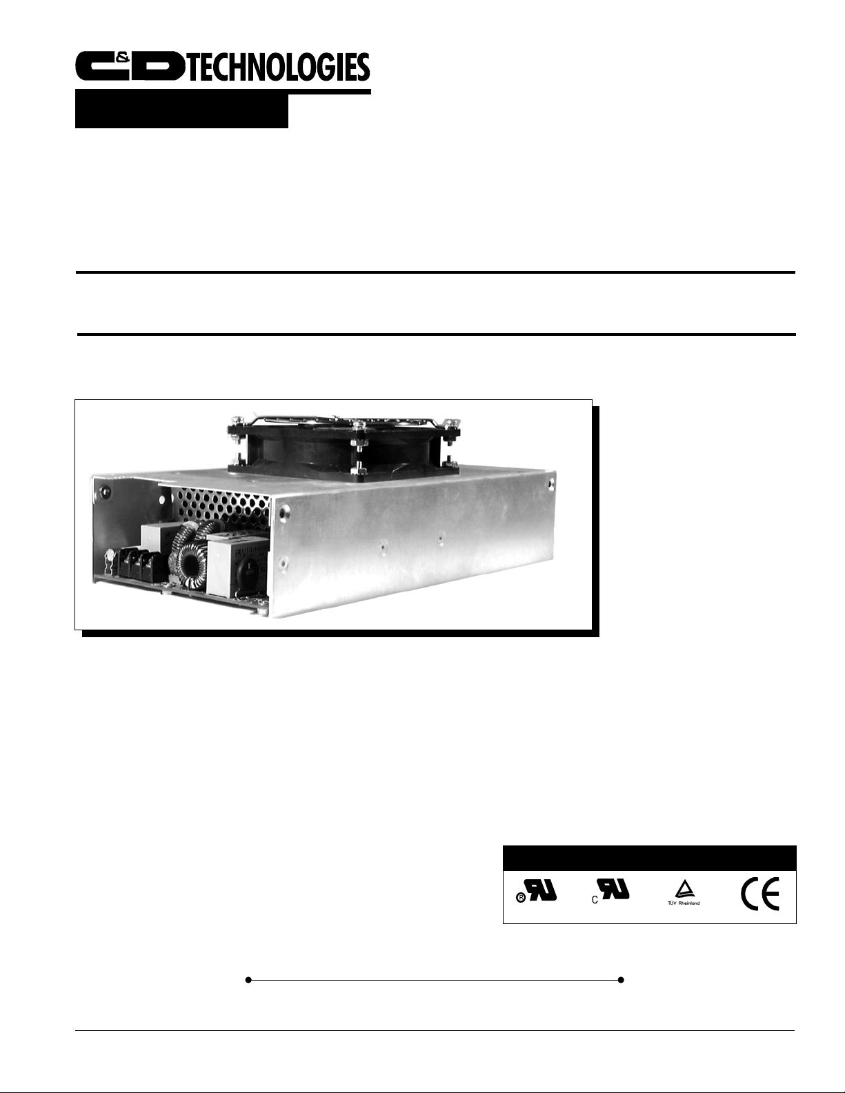
DESCRIPTION
The SX500 is a compact 500 watt Power Factor
Corrected, single output power supply. Active cur-
Active Current Sharing With ORing Diodes
FCC/VDE Class B EMI Filter
Optional Active Inrush Current Limit
Compact Size: 10” x 4.85” x 2.19”
Optional SCR Crowbar
Optional Cover With Fan
Internet: http://www.cdpowerelectronics.com
Power Electronics Division, United States
3400 E Britannia Drive, Tucson, Arizona 85706
Phone: 520.295.4100 Fax: 520.770.9369
SX500 10/98 REV B Page 1
rent sharing circuitry with ORing diodes, together with
control functions and alarm options, simplifies N+1
redundant applications.
AGENCY APPROVALS
Power Electronics Division, Europe
C&D Technologies (Power Electronics) Ltd.
132 Shannon Industrial Estate, Shannon, Co. Clare, Ireland
Tel: +353.61.474.133 Fax:+353.61.474.141
Page 2
Input Specifications
Parameter Conditions Min Typ Max Units
Operating Range 47-63 Hz 90 264 VAC
Inrush Current Limiting
Thermistor 120 V
Active Current Limit 264 VAC 19 APK
Efficiency Nominal line and full load 75 %
Power Factor Correction (PFC) 0.99
Meets EN61000-3-2 (formerly IEC 555-2)
AC, cold start 30 APK
240 VAC, cold start 60 APK
Remote Sense
Remote Sense is provided and will compensate for 1.0V
of line drop. Remote Sense leads are protected against
open, short and reversal.
Remote On/Off (Optional)
The power supply is turned on with a TTL logic ‘1’ (or open)
signal and turned off by a switch closure or TTL logic ‘0’
referenced to (-) sense terminal. Consult the factory for
other options.
Over Voltage Protection
Output #1: 115% of nominal voltage is typical.
The power supply will latch off until AC power is cycled.
Over Current Protection
Automatic recovery upon fault removal.
Transient Response
The peak output voltage excursion will not exceed 2% and
will recover within 1% in 200 µsec for a 25% step load.
Reverse Voltage Protection
The output is protected to rated load.
Power Fail Signal
Upon AC input voltage removal, the power fail signal drops
to logic zero at least 10msec before loss of DC output.
Upon AC input turn-on, signal remains low until output is in
regulation. Consult the factory for other options.
N+1 Load Share
Output has active load sharing circuitry. Units will load
share within 1% of the Maximum Rated Load.
Over Temperature Protection
Thermal switch turns off power supply if overheating occurs
and automatically restarts.
Safety
UL/CUL Recognized: UL File Number E13164 (1950)
TUV License Number: R9773309 (EN60950) (IEC950)
Cooling
The unit is designed to operate with 30 CFM of airflow.
DC Power Good Signal
The signal is activated by a ±10% loss of regulation Active
low or high; TTL Level; common with (-) sense. Consult the
factory for other options.
SX500 10/98 REV BPage 2
Page 3

Output Voltages and Maximum Rated Loads
OUTPUT
MODEL NUMBER V
SX500-U1A ±24V 21A 26A
SX500-U1B ±28V 18A 22A
SX500-U1C ±36V 14A 17A
SX500-U1D ±48V 10.5A 12.5A
OUT IMAX IPK
Output Specifications
Parameter Limits
Regulation
Line ± 0.2%
Load ±0.5%
Minimum Load 0.1A
Hold-Up Time 20mSec at Full Load
Parameter Conditions Min Typ Max Units
Voltage Adjustment Range ±5 %
PARD 20 MHz bandwidth 0.5 % P-P
Temperature
Operating 050°C
Storage -20 +85 °C
Temperature Coefficient (TC) After half hour warm-up ± 0.02 % /°C
SX500 10/98 REV B Page 3
Page 4

Mechanical
0.700
0.550
3.900
8.500
10.00
6-32 THD
(4x)
4.850
2.148
PIN 1
J9
PIN 1
TB2
1.300
AIR FLOW
0.040
COVER
0.620
3.190
NOTES:
All measurements are in inches
FAN MOUNTED ON COVER ADDS 1.30”.
COOLING: The SX500 is designed to operate with 30 CFM airflow.
SHOCK AND VIBRATION: The SX500 family meets the requirements of MIL STD-810D. (Vibration-Method 514.3 Procedure 1. Shock-Method 516.3 Procedure 1.)
WEIGHT: Approximately 4 lbs.
Pin Specifications
Terminal Block 1 Terminal Block 2
POS FUNCTION POS FUNCTION
1 Ground 1 +V
2 AC Neutral 2 +V
3 AC Line 3 -V
4-V
Connector Specifications
J9 Connector
Molex No. 22-28-1093
PIN FUNCTION
1 - Sense
2 + Sense
3 Current Share
4 Remote Inhibit
5Power Fail
6 DC OK
7 Sync
8 Signal Ground
9N/C
Standard Options are shown, consult factory for other available options.
The information provided herein is believed to be reliable; however, C&D TECHNOLOGIES assumes no responsibility for inaccuracies or omissions. C&D TECHNOLOGIES
assumes no responsibility for the use of this information, and all use of such information shall be entirely at the user’s own risk. Prices and specifications are subject to
change without notice. No patent rights or licenses to any of the circuits described herein are implied or granted to any third party. C&D TECHNOLOGIES does not authorize
or warrant any C&D TECHNOLOGIES product for use in life support devices/systems or in aircraft control applications.
SX500 10/98 REV BPage 4
 Loading...