

Page 1
SWR200
Precision
Sine Wave Reference
THALER CORPORATION • 2015 N. FORBES BOULEVARD • TUCSON, AZ. 85745 • (520) 882-4000
FEATURES
•• VERY HIGH ACCURACY: 7.071 Vrms ±0.05%
•• EXTREMELY LOW DRIFT:
3 ppm/°C (-55°C to +125°C)
•• EXCELLENT STABILITY: 10 ppm/1000 Hrs. Typ.
•• LOW DISTORTION:
0.1% THD @ f = 3300 Hz
•• HERMETIC 14-PIN CERAMIC DIP
•• MILITARY PROCESSING OPTION
DESCRIPTION
SWR200 is a Precision Sine Wave Reference
providing an ultra stable sine wave output of
7.071V at ±0.05% initial accuracy and
temperature coefficient as low as 3 ppm/°C over
the full military temperature range. The extreme
accuracy is made possible by a chopper-based
AGC circuit. The temperature characteristic of the
chopper circuit compensates the typical
nonlinearity of the internal DC zener reference,
resulting in a nearly linear amplitude-temperature
characteristic. Frequency of the SWR200 is
programmable with two external capacitors.
APPLICATIONS
•• TRANSDUCER EXCITATION
•• HIGH RESOLUTION SERVO SYSTEMS
•• HIGH PRECISION TEST and
MEASUREMENT INSTRUMENTS
•• AC VOLTAGE STANDARD
•• LVDT OR RVDT REFERENCE
•• MULTIPLYING D/A REFERENCE
SELECTION GUIDE
Type
SWR200C 7.071V -25°C to +85°C DIP
Output
(Typ.)
Temperature
Operating Range
Package
The SWR200 is available in a 14-pin bottom
braze package. They are hermetically sealed and
"M" versions are screened for high reliability and
quality.
SWR200 is well suited for any application
requiring a stable sine wave source. The SWR200
can be used as a reference source in precision
sensing systems based on LVDT or RVDT
position sensors. A programmable AC reference
can be constructed using the SWR200 as a
reference for a high accuracy multiplying Digital to
Analog Converter.
SWR200M 7.071V -55°C to +125°C DIP
SWR200DS REV. D JUNE 1995
Page 2
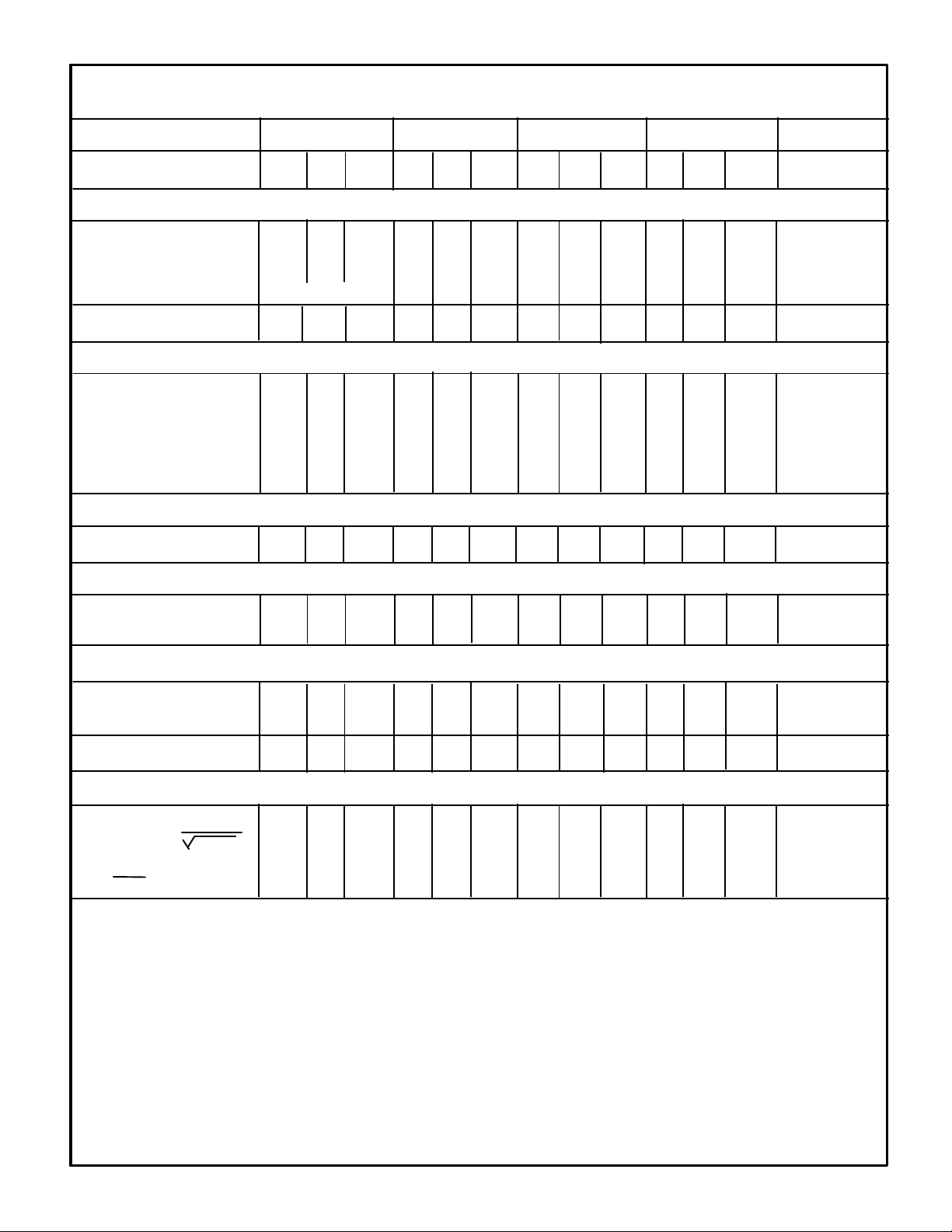
ELECTRICAL SPECIFICATIONS
Vps =±15V, T = 25°C, RL = 10KΩ unless otherwise noted.
SWR200
MODEL C M
PARAMETERS MIN TYP MAX MIN TYP MAX MIN TYP MAX MIN TYP MAX UNITS
ABSOLUTE MAXIMUM RATINGS
Power Supply ±13.5 15 ±22 * * V
Operating Temperature -25 85 -55 125 °C
Storage Temperature -65 150 * * °C
Short Circuit Protection Continuous *
OUTPUT VOLTAGE 7.071 * Vrms
OUTPUT VOLTAGE ERRORS
Initial Error 0.05 * %
Warmup Drift 100 * µV
DC Offset 3 * mV
DC Offset Over Temp. 3 18 * * µV/°C
Tmin - Tmax 1 2.0 1 3.0 ppm/°C
Long-Term Stability 10 * ppm/°C
OUTPUT CURRENT
Range ±10 * mA
REGULATION
Line 10 * ppm/V
Load 3 * ppm/mA
POWER SUPPLY CURRENTS
+PS 10.5 13 * * mA
-PS 9.5 13 * * mA
DISTORTION 0.5 * %
FREQUENCY
-5
10
Range (f)
f =
∇
vs. Temperaturef
f
C1 C2
.98 1 1.02 * * * Hz
400 10K * Hz
15 * ppm/°C
NOTES:
3.Pin 8 is internally connected to Pin 7 and can be
*Same as C Models.
1.Using the box method, the specified value is the
maximum deviation from the output voltage at 25°C
over the specified operating temperature range.
2.The specified values are unloaded.
used as Ref. GND.
4. The frequency range can be extended to any desired
lower value by using 2 external AGC capacitors (see
AN-3).
5.The increase in distrotion at lower frequencies can be
eliminated by using external AGC capacitors (see
AN-3).
SWR200DS REV. D JUNE 1995
Page 3

TYPICAL PERFORMANCE CURVES
V
vs. TEMPERATURE
OUT
Temperature oC
SWR200C
DISTORTION VS. TEMP
V
vs. TEMPERATURE
OUT
Temperature oC
SWR200L
% ∆∆ FREQ. vs. TEMP.
Temperature oC
DISTORTION vs. FREQUENCY
SWR200C
% ∆∆ FREQ. vs. TEMP.
Temperature oC
SWR200L
NORMALIZED DISTORTION vs. C2/C1
Temperature oC
POWER SUPPLY CURRENT vs. TEMP.
Temperature oC
Frequency (Hz)
CASE TEMP. RISE ABOVE AMBIENT
vs. OUTPUT CURRENT
Output Current (mA)
C2/C1
JUNCTION TEMP. RISE
ABOVE CASE TEMP. vs
OUTPUT CURRENT
Output Current (mA)
SWR200DS REV. D JUNE 1995
Page 4

DISCUSSION OF PERFORMANCE
THEORY OF OPERATION
The following refers to the schematic in Figure 1.
A1 and A2 are connected as a phase-shift oscillator
circuit with the frequency set by the external
capacitors C1 and C2. Q4 is included in the
feedback loop of A1 as a gain control element.
The oscillator output is fed to the chopper amplifier
which develops an absolute value representation of
the oscillator output. The chopper output is
compared to a precision DC reference in integrator
amplifier A3. This DC error signal is used ot control
the gain setting FET Q4.
As in all precision zener based DC references, the
drift of the zener becomes nonlinear at temperature
extremes. The chopper amplifier drift characteristic
is complementary to this nonlinearity and
compensates for the reference drift.
APPLICATION INFORMATION
Figure 1 shows the connections for the SWR200
including the two frequency setting capacitors. The
frequency is:
-5
f =
10
C C
1
2
The frequency stability is directly related to the
stability of the capacitors, therefore stable capacitors
like NPO ceramic, or polycarbonate or polystyrene
film should be used.
Two separate ground pins are provided for
accurate ground sensing. This minimizes errors due
to drops in the ground pin which can become a
significant source of error in sockets.
The offset of the SWR200 is fully specified for
initial offset and drift and is low enough that it can
normally be neglected. In applications which are
especially sensitive to offset the output can be AC
coupled. Proper capacitor sizing and high impedance
sensing will minimize errors due to capacitive
coupling.
SCHEMATIC
FIGURE 1
SWR200DS REV. D JUNE 1995
Page 5

FIGURE 2
EXTERNAL CONNECTIONS
PIN CONFIGURATION
TOP VIEW
PACKAGE
C1
C1
-PS
NC
NC
NC
GND
SWR200
C2
C2
+PS
NC
NC
OUTPUT
GND SENSE
MECHANICAL
INCHES MILLIMETER14-PIN HYBRID
DIM MIN MAX MIN MAX DIM MIN MAX MIN MAX
E .480 .500 12.1 12.7 A .120 .155 3.0 4.0
L .195 .215 4.9 5.4 Q .015 .035 0.4 0.9
D .775 .805 19.7 20.4 Q1 N/A .030 N/A 0.7
B .016 .020 0.4 0.5 C .009 .012 0.2 0.3
B1 .038 .042 0.9 1.0 G1 .290 .310 7.3 7.8
B2 .095 .105 2.4 2.6
S .085 .105 2.1 2.6
P .004 .006 0.10 0.15
INCHES MILLIMETER
SWR200DS REV. D JUNE 1995
 Loading...