

Page 1
®
N - CHANNEL 1000V - 1.2Ω - 8A - TO-247
TYPE V
DSS
STW8NB100 1000 V < 1.5 Ω 8 A
■
TYPICAL R
■
EXTREMELY HIGH dv/dt CAPABILITY
■
30V GATE TO SOURCE VOLTAGE RATING
±
■
100% AVALANCHE TESTED
■
LOW INTRINSIC CAPACITANCE
■
GATE CHARGE MINIMIZED
■
REDUCED VOLTAGE SPREAD
DS(on)
= 1.2
R
DS(on)
Ω
STW8NB100
PowerMESH MOSFET
PRELIMINARY DATA
I
D
3
2
1
DESCRIPTION
Using the latest high voltage MESH OVERLAY
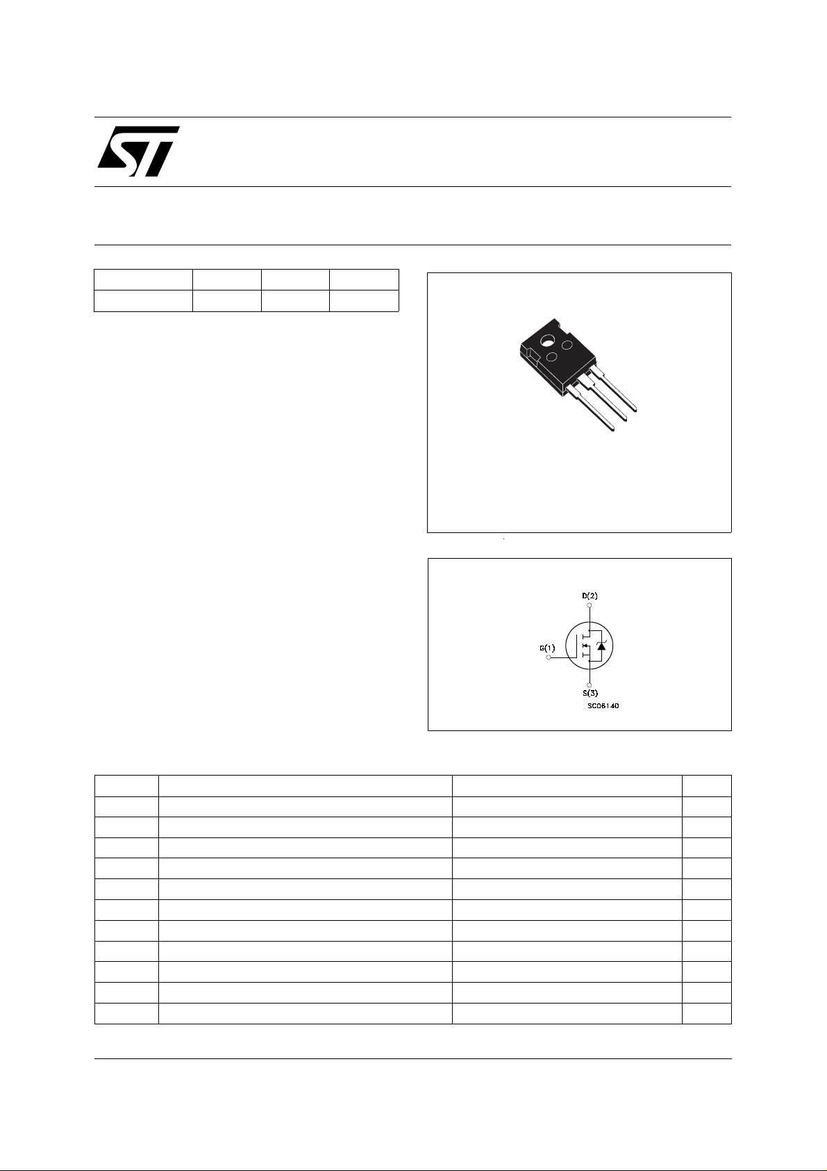
TO-247
process, STMicroelectronics has designed an advanced family of power MOSFETs with outstanding performances. The new patent pending st rip
layout coupled with the Company’s proprietary
edge termination structure, gives the lowest
RDS(on) per area, exceptional avalanche and
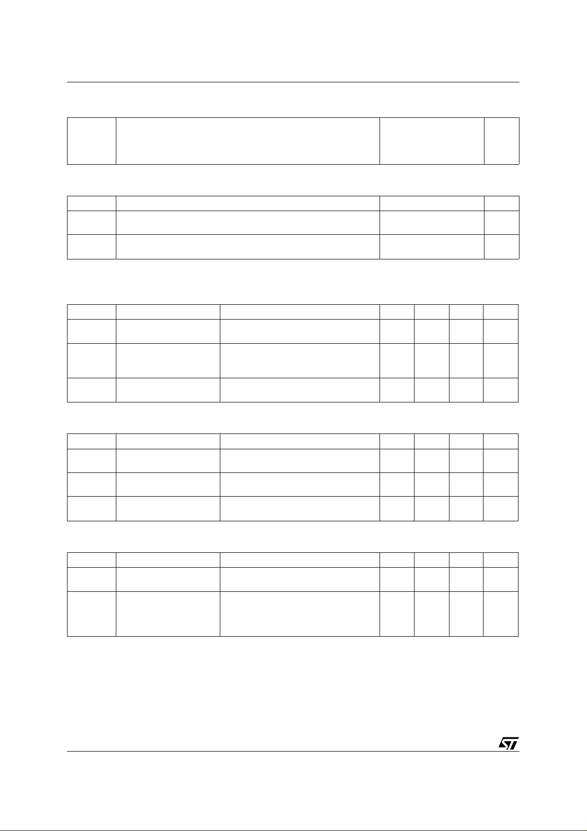
INTERNAL SCHEMATIC DIAGRAM
dv/dt capabilities and unrivalled gate charge and
switching characteristics.
APPLICATIONS
■
HIGH CURRENT, HIGH SPEED SWITCH ING
■
SWITCH MODE POWER SUPPLY (SMPS)
■
DC-AC CONVERTER FOR WELDING
EQUIPMENT AND UNINTERRUPTA BLE
POWER SUPPLY AND MOTOR DRIVE
ABSOLUTE MAXIMUM RATINGS
Symbol Parameter Value Unit
V
V
V
I
DM
P
dv/dt
T
(•) Pulse width limited by safe operating area (1) ISD
March 1999
Drain-source Voltage (VGS = 0) 1000 V
DS
Drain- gate Voltage (RGS = 20 kΩ)
DGR
Gate-source Voltage ± 30 V
GS
I
Drain Current (continuous) at Tc = 25 oC8A
D
I
Drain Current (continuous) at Tc = 100 oC5A
D
1000 V
(•) Drain Current (pulsed) 32 A
Total Dissipation at Tc = 25 oC 190 W
tot
Derating Factor 1.52 W/
Peak Diode Recovery voltage slope 4 V/ns
(1)
Storage Temperature -65 to 150
stg
T
Max. Operating Junction Temperature 150
j
≤8 Α,
di/dt ≤ 200 A/µs, VDD ≤ V
(BR)DSS
, Tj ≤ T
JMAX
o
C
o
C
o
C
1/5
Page 2
STW8NB100
THERMAL DATA
R
thj-case
R
thj-amb
R
thc-sink
T
Thermal Resistance Junction-case Max
Thermal Resistance Junction-ambient Max
Thermal Resistance Case-sink Typ
Maximum Lead Temperature For Soldering Purpose
l
AVALANCHE CHARACTERIST ICS
Symbol Parameter Max Value Unit
I
AR
E
Avalanche Current, Repetitive or Not-Repetitive
(pulse width limited by T
Single Pulse Avalanche Energy
AS
(starting T
= 25 oC, ID = IAR, V
j
max)
j
DD
= 50 V)
0.66
30
0.1
300
8A
600 mJ
o
C/W
o
C/W
o
C/W
o
C
ELECTRICAL CHARACTERISTICS
= 25 oC unless otherwise specified)
(T
case
OFF
Symbol Parameter Test Conditions Min. Typ. Max. Unit
V
(BR)DSS
Drain-source
I
= 250 µA V
D
GS
= 0
1000 V
Breakdown Voltage
I
DSS
I
GSS
Zero Gate Voltage
Drain Current (V
GS
Gate-body Leakage
Current (V
DS
= 0)
= 0)
= Max Rating
V
DS
V
= Max Rating Tc = 125
DS
o
C
V
= ± 30 V
GS
1
50
± 100 nA
ON (∗)
Symbol Parameter Test Conditions Min. Typ. Max. Unit
V
GS(th)
Gate Threshold
V
= VGS ID = 250 µA
DS
345V
Voltage
R
DS(on)
Static Drain-source On
VGS = 10 V ID = 4 A 1.2 1.5 Ω
Resistance
I
D(on)
On State Drain Current VDS > I
V
= 10 V
GS
D(on)
x R
DS(on)max
8A
DYNAMIC
Symbol Parameter Test Conditions Min. Typ. Max. Unit
g
(∗) Forward
fs
Transconductance
C
C
C
Input Capacitance
iss
Output Capacitance
oss
Reverse Transfer
rss
Capacitance
VDS > I
V
DS
x R
D(on)
DS(on)max
= 25 V f = 1 MHz V
ID = 4 A 8.9 S
= 0 2900
GS
275
27
µA
µA
pF
pF
pF
2/5
Page 3
STW8NB100
ELECTRICAL CHARACTERISTICS
(continued)
SWITCHING ON
Symbol Parameter Test Conditions Min. Typ. Max. Unit
t
d(on)
Q
Q
Q
Turn-on Time
Rise Time
t
r
Total Gate Charge
g
Gate-Source Charge
gs
Gate-Drain Charge
gd
V
= 500 V ID = 3.5 A
DD
= 4.7 Ω VGS = 10 V
R
G
V
= 800 V ID = 7 A V
DD
= 10 V 68
GS
32
13
95 nC
16
31
SWITCHING OFF
Symbol Parameter Test Conditions Min. Typ. Max. Unit
t
r(Voff)
t
t
Off-voltage Rise Time
Fall Time
f
Cross-over Time
c
V
= 800 V ID = 7 A
DD
= 4.7 Ω VGS = 10 V
R
G
32
32
40
SOURCE DRAIN DIODE
Symbol Parameter Test Conditions Min. Typ. Max. Unit
8
32
I
SDM
I
SD
Source-drain Current
(•)
Source-drain Current
(pulsed)
V
(∗) Forward On Voltage ISD = 8 A VGS = 0 1.6 V
SD
t
Q
Reverse Recovery
rr
Time
Reverse Recovery
rr
I
= 8 A di/dt = 100 A/µs
SD
V
= 100 V Tj = 150 oC
DD
1000
11
Charge
I
RRM
Reverse Recovery
21
Current
(∗) Pulsed: Pulse duration = 300 µs, duty cycle 1.5 %
(•) Pulse width limited by safe operating area
ns
ns
nC
nC
ns
ns
ns
A
A
ns
µC
A
3/5
Page 4
STW8NB100
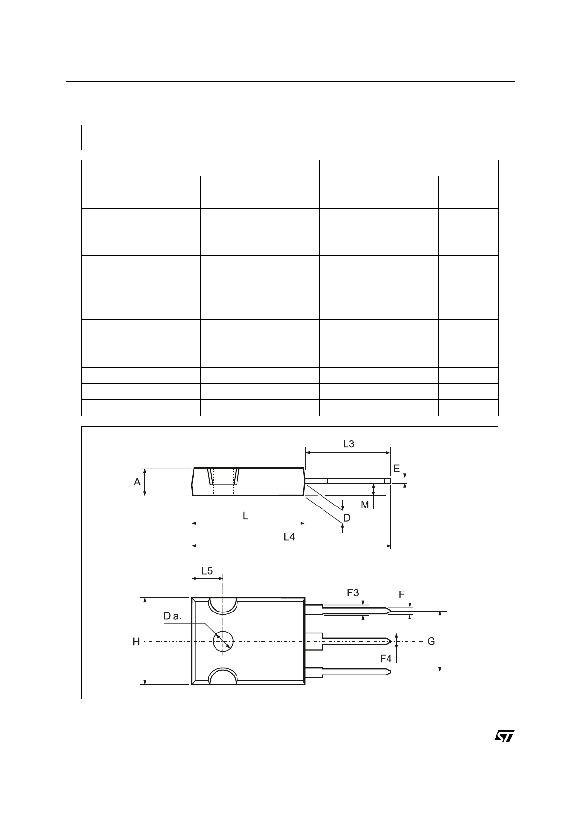
TO-247 MECHANICAL DATA
DIM.
MIN. TYP. MAX. MIN. TYP. MAX.
A 4.7 5.3 0.185 0.209
D 2.2 2.6 0.087 0.102
E 0.4 0.8 0.016 0.031
F 1 1.4 0.039 0.055
F3 2 2.4 0.079 0.094
F4 3 3.4 0.118 0.134
G 10.9 0.429
H 15.3 15.9 0.602 0.626
L 19.7 20.3 0.776 0.779
L3 14.2 14.8 0.559 0.413 0.582
L4 34.6 1.362
L5 5.5 0.217
M 2 3 0.079 0.118
Dia 3.55 3.65 0.140 0.144
mm inch
4/5
P025P
Page 5

STW8NB100
Information f urnished i s believed t o be accurate an d reliabl e. How ever, STMicroelect ronics assu mes no responsib ility fo r the consequen ces
of use of such information nor for any infringement of patents or other rights of third parties which may result from its use. No license is
granted by implication or otherwise under any patent or patent rights of STMicroelectronics. Specification mentioned in this publication are
subject to chan ge w ithout notice. This publicatio n su persedes a nd r eplaces al l inf ormati on previ ously suppl ied. STMicroelect ron ics produ cts
are not auth ori zed f or use as critical component s in life support devices or systems without express written ap proval o f STM icroelectronics.
The ST logo is a trademark of STMicroelectronics
© 1999 STMicroelectro nics – Printed in Ita ly – All Rights Re served
STMicroele ct ronics GROUP OF COMPANIES
Australia - Brazil - Canada - China - France - Germany - Italy - Japan - Korea - Malaysia - Malta - Mexico - Morocco - The Netherlands -
Singapore - Spain - Sweden - Sw itzerland - Taiwan - Thailand - United Kingdom - U.S.A.
http://www.st.com
.
5/5
 Loading...