

Page 1
STW8NA80
N - CHANNEL ENHANCEMENT MODE
TYPE V
STW8NA80
ST H8NA80FI
■ TYPICALR
■ ± 30V GATE TO SOURCE VOLTAGERATING
■ 100%AVALANCHETESTED
■ REPETITIVEAVALANCHEDATA AT 100
■ LOW INTRINSICCAPACITANCES
■ GATEGHARGEMINIMIZED
■ REDUCEDTHRESHOLD VOLTAGE SPREAD
DS(on)
DSS
800 V
800 V
= 1.3 Ω
DESCRIPTION
This series of POWER MOSFETSrepresents the
most advanced high voltage technology. The optimized cell layout coupled with a new proprietary
edge termination concur to give the device low
RDS(on) and gate charge, unequalled ruggednessand superiorswitchingperformance.
R
DS(on)
<1.50Ω
<1.50Ω
I
D
7.2 A
4.5 A
o
C
STH8NA80FI
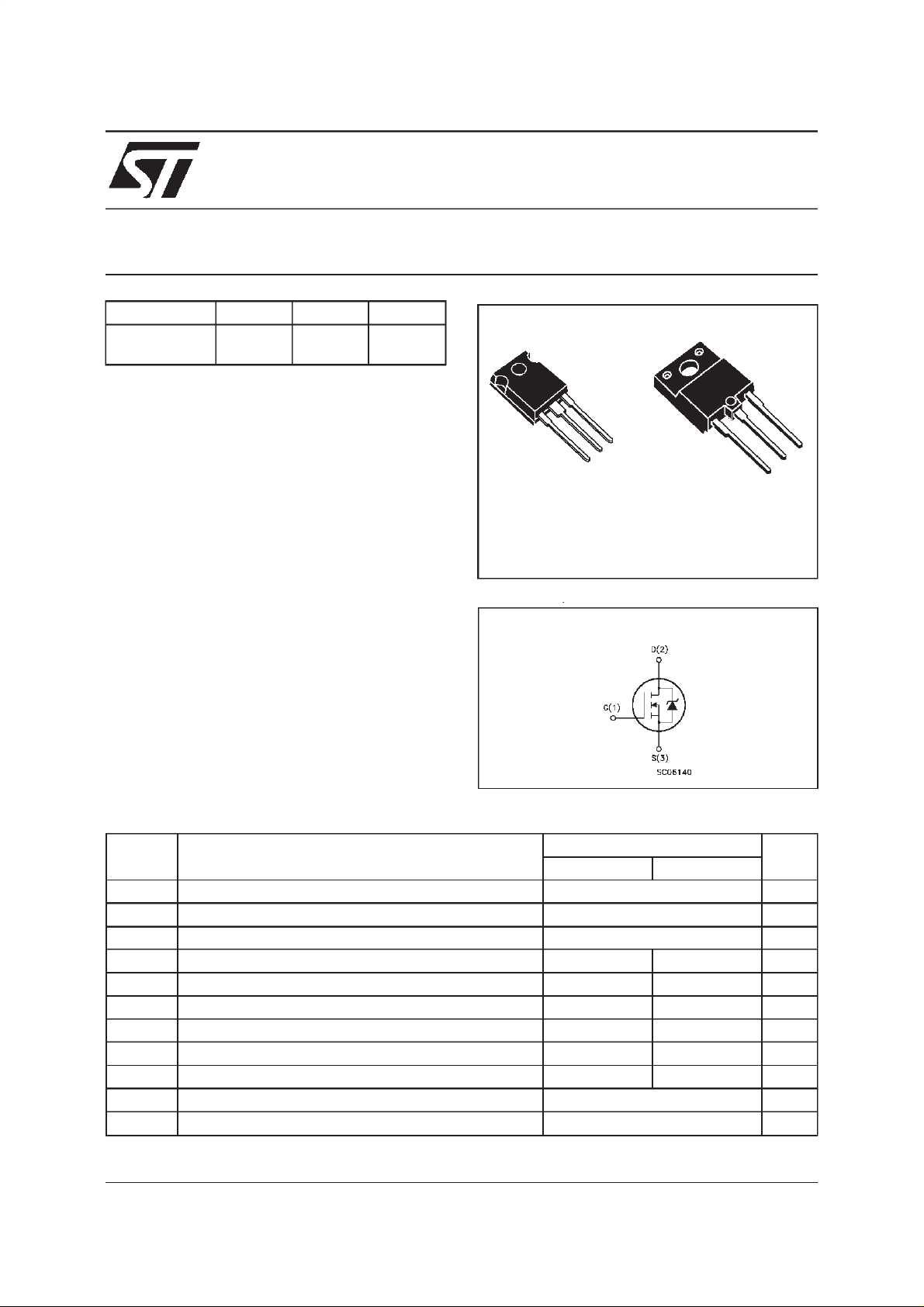
POWER MOS TRANSISTORS
PRELIMINARY DATA
3
2
1
TO-247 ISOWATT218
INTERNAL SCHEMATIC DIAGRAM
3
2
1
APPLICATIONS
■ HIGHCURRENT, HIGH SPEEDSWITCHING
■ SWITCHMODE POWER SUPPLIES (SMPS)
■ DC-AC CONVERTERS FOR WELDING
EQUIPMENTANDUNINTERRUPTIBLE
POWERSUPPLIESAND MOTORDRIVE
ABSOLUTE MAXIMUM RATINGS
Symb o l Parame t er Val ue Unit
ST W8NA80 STH8N A80 F I
V
V
V
I
DM
P
Drain-sourc e Voltage (VGS=0)
DS
Drain- ga t e Voltage (RGS=20kΩ)
DGR
Gate-s ource Voltage
GS
I
Drain Cur rent ( c ont i nuous) at Tc=25oC
D
I
Drain Cur rent ( c ont i nuous) at Tc= 100oC
D
(•)
Drain Cur rent ( puls e d)
Total Dissipation at Tc=25oC
tot
Derating Factor
V
T
(•) Pulse width limited by safe operating area
Ins ula t ion Withst and Volta ge (DC)
ISO
St orage Temper ature
stg
T
Max. Operating Junct ion Temperatu re
j
7.2 4.5 A
4.5 2.8 A
28.8 28.8 A
175 70 W
1.4 0.56 W/
800 V
800 V
± 30 V
4000 V
-65 to 150
150
o
C
o
C
o
C
October 1998
1/6
Page 2
STW8NA80 STH8NA80FI
THERMAL DATA
TO-247 ISOWATT218
R
thj-case
R
thj-amb
R
thc-sink
T
Ther mal Resistanc e Junct ion-case Max
Ther mal Resistanc e Junct ion-ambient Max
Ther mal Resistanc e Case-sink Ty p
Maximum Lead T e m pe ra t ure For Soldering P urpose
l
AVALANCHE CHARACTERISTICS
Symbol Parameter Max V alue Unit
I
AR
E
Avalanche C urrent, Repetitive or Not-Repetitive
(pulse width limited by T
Single Pul se Avalanc he Ener gy
AS
(starting T
=25oC, ID=IAR,VDD=50V)
j
max,δ <1%)
j
0.71 1.78
30
0.1
300
7.2 A
700 mJ
o
C/W
o
C/W
o
C/W
o
C
ELECTRICAL CHARACTERISTICS
=25oC unless otherwisespecified)
(T
case
OFF
Symbol Parameter Test Conditions Min. Typ. Max. Unit
V
(BR)DSS
I
DSS
I
GSS
Drain-source
Break dow n Vo lt age
Zero Gate Voltage
Drain Curre nt (V
GS
Gat e- bod y Leakag e
Current (V
DS
=0)
=0)
=250µAVGS=0
I
D
V
=MaxRating
DS
=MaxRating Tc= 100oC
V
DS
V
= ± 30 V
GS
800 V
50
500
100 nA
ON(∗)
Symbol Parameter Test Conditions Min. Typ. Max. Unit
V
GS(th)
R
DS(on)
I
D(on)
Gate Threshold Voltage VDS=VGSID= 250µA
Sta t ic Drain-s our c e On
Resistance
On State Drain Current
V
=10V ID=4A
GS
V
DS>ID(on)xRDS(on)max
VGS=10V
2.25 3 3.75 V
1.3 1. 5
7.2 A
DYNAMIC
Symbol Parameter Test Conditions Min. Typ. Max. Unit
g
(∗)Forward
fs
Tr ansc on duc tance
C
C
C
Input Capaci t ance
iss
Out put Capac itance
oss
Reverse Transfer
rss
Capacit a nc e
V
DS>ID(on)xRDS(on)maxID
=25V f=1MHz VGS=0
V
DS
=4A
4.5 7.9 S
1750
188
50
2300
245
70
µA
µA
Ω
pF
pF
pF
2/6
Page 3

STW8NA80 STH8NA80FI
ELECTRICAL CHARACTERISTICS
(continued)
SWITCHINGON
Symbol Parameter Test Conditions Min. Typ. Max. Unit
t
d(on)
t
r
(di/dt)
Q
Q
gs
Q
gd
Turn-on Time
Rise Time
on
Tur n-on Current Slope
Tot al Gate Charge
g
Gat e- Source Charge
Gate-Drain Charge
VDD=400V ID=4A
=4.7 Ω VGS=10V
R
G
V
=640V ID=8A
DD
=47
R
V
Ω
G
= 400 V ID=8A VGS=10V
DD
VGS=10V
20
28
170 A/µ s
75
10
35
28
38
100 nC
SWITCHINGOFF
Symbol Parameter Test Conditions Min. Typ. Max. Unit
t
r(Voff)
t
t
Off-voltage Rise T ime
Fall T ime
f
Cross-over Tim e
c
VDD=640V ID=8A
R
=4.7
G
Ω
VGS=10V
18
20
25
25
28
35
SOURCEDRAINDIODE
Symbol Parameter Test Conditions Min. Typ. Max. Unit
I
SD
I
SDM
V
SD
t
Q
I
RRM
(∗) Pulsed:Pulse duration = 300 µs, duty cycle 1.5 %
(•) Pulse width limited by safe operatingarea
Source-drain Current
(•)
Source-drain Current
(pulsed)
(∗)
For ward On Volta ge I
Reverse Recovery
rr
Time
Reverse Recovery
rr
Charge
Reverse Recovery
Current
=7.2A VGS=0
SD
ISD=7.5A di/dt=100A/µs
= 100 V Tj=150oC
V
DD
7.2
28.8
1.6 V
850
17
40
ns
ns
nC
nC
ns
ns
ns
A
A
ns
µ
A
C
3/6
Page 4

STW8NA80 STH8NA80FI
TO-247 MECHANICAL DATA
DIM.
MIN. TYP. MAX. MIN. TYP. MAX.
A 4.7 5.3 0.185 0.209
D 2.2 2.6 0.087 0.102
E 0.4 0.8 0.016 0.031
F 1 1.4 0.039 0.055
F3 2 2.4 0.079 0.094
F4 3 3.4 0.118 0.134
G 10.9 0.429
H 15.3 15.9 0.602 0.626
L 19.7 20.3 0.776 0.779
L3 14.2 14.8 0.559 0.413 0.582
L4 34.6 1.362
L5 5.5 0.217
M 2 3 0.079 0.118
Dia 3.55 3.65 0.140 0.144
mm inch
4/6
P025P
Page 5

ISOWATT218MECHANICAL DATA
STW8NA80 STH8NA80FI
DIM.
mm inch
MIN. TYP. MAX. MIN. TYP. MAX.
A 5.35 5.65 0.210 0.222
C 3.3 3.8 0.130 0.149
D 2.9 3.1 0.114 0.122
D1 1.88 2.08 0.074 0.081
E 0.75 1 0.029 0.039
F 1.05 1.25 0.041 0.049
G 10.8 11.2 0.425 0.441
H 15.8 16.2 0.622 0.637
L1 20.8 21.2 0.818 0.834
L2 19.1 19.9 0.752 0.783
L3 22.8 23.6 0.897 0.929
L4 40.5 42.5 1.594 1.673
L5 4.85 5.25 0.190 0.206
L6 20.25 20.75 0.797 0.817
M 3.5 3.7 0.137 0.145
N 2.1 2.3 0.082 0.090
U 4.6 0.181
L3
N
E
A
D
C
L5
M
H
L2
L6
L1
D1
F
U
G
123
L4
P025C
5/6
Page 6

STW8NA80 STH8NA80FI
Information furnished is believed to be accurate and reliable. However, STMicroelectronics assumes no responsibility for the consequences
of use of such information nor for any infringement of patents or other rights of third parties which may result from its use. No license is
granted by implicationor otherwise under any patent or patent rights of STMicroelectronics. Specification mentioned in this publication are
subject to change without notice. This publication supersedes and replaces all information previously supplied. STMicroelectronics products
are not authorized for use as critical components in life support devices or systems without express written approval of STMicroelectronics.
The ST logo is a trademarkof STMicroelectronics
1998 STMicroelectronics – Printed in Italy – All Rights Reserved
STMicroelectronics GROUP OF COMPANIES
Australia - Brazil - Canada -China - France -Germany - Italy - Japan - Korea - Malaysia - Malta - Mexico - Morocco - The Netherlands -
Singapore - Spain - Sweden - Switzerland - Taiwan - Thailand - United Kingdom - U.S.A.
http://www.st.com
.
6/6
 Loading...