

Page 1
STW80NE06-10
N - CHANNEL 60V - 0.0085Ω - 80A - TO-247
STripFET ” POWER MOSFET
TYPE V
DSS
R
DS(on)
I
D
STW80NE06 -1 0 60 V <0. 01 Ω 80 A
■ TYPICALR
■ EXCEPTIONALdv/dt CAPABILITY
■ 100% AVALANCHETESTED
■ APPLICATIONORIENTED
DS(on)
=0.0085 Ω
CHARACTERIZATION
DESCRIPTION
This Power MOSFET is thelatestdevelopment of
STMicroelectronics unique ”Single Feature
Size” strip-based process. The resulting
transistor shows extremely high packing density
for low on-resistance, rugged avalanche
characteristics and less critical alignment steps
therefore a remarkable manufacturing
reproducibility.
APPLICATIONS
■ SOLENOIDANDRELAY DRIVERS
■ MOTORCONTROL, AUDIOAMPLIFIERS
■ DC-DCCONVERTERS
■ AUTOMOTIVE ENVIRONMENT
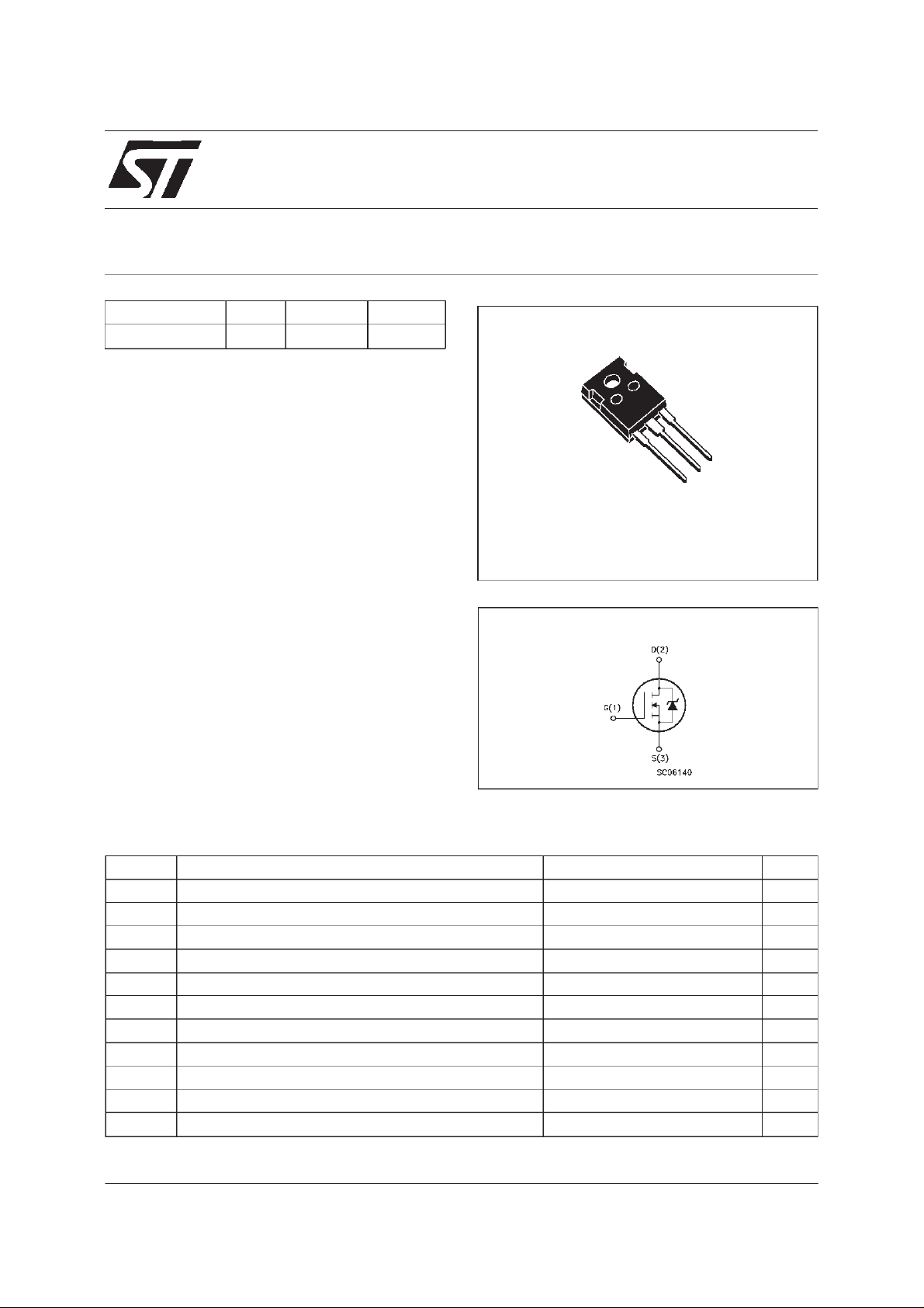
3
2
1
TO-247
INTERNAL SCHEMATIC DIAGRAM
ABSOLUTE MAXIMUM RATINGS
Symb o l Para meter Value Uni t
V
V
V
I
DM
P
dv/ dt Peak Di ode Recovery voltage slope 7 V/ns
T
(•) Pulse width limitedby safe operating area (1)ISD≤ 80 A,di/dt ≤ 300 A/µs, VDD≤ V
July 1998
Drain-source V oltage (VGS=0) 60 V
DS
Drain- gate Voltage (RGS=20kΩ)
DGR
Gat e- source Voltage ± 20 V
GS
I
Drain Current ( continuous) at Tc=25oC80A
D
I
Drain Current ( continuous) at Tc=100oC57A
D
60 V
(•) Dr a in Current (pulsed) 320 A
Tot al D iss ip at i on at Tc=25oC200W
tot
Derating Factor 1.33 W/
Sto rage Temperature -65 to 175
stg
T
Max. O peratin g J u nc tion T e m perature 175
j
(BR)DSS,Tj≤TJMAX
o
C
o
C
o
C
1/8
Page 2
STW80NE06-10
THERMAL DATA
R
thj-case
Rthj-a m b
R
thc-sin k
T
AVALANCHE CHARACTERISTICS
Symbol Para met e r Max Value Unit
I
AR
E
Ther mal Resist ance Junction- case Max
Ther mal Resist ance Junction- ambient Max
Ther mal Resist ance Case-sink Ty p
Maximum Lea d Te mperat ure Fo r S oldering Purpos e
l
Avalanche Current , Repetit i v e or Not -R e petitive
(pulse width limited b y T
Single Pulse Avalanche Energy
AS
(starting T
=25oC, ID=IAR,VDD=30V)
j
max)
j
0.75
30
0.1
300
80 A
350 mJ
o
C/W
oC/W
o
C/W
o
C
ELECTRICAL CHARACTERISTICS (T
=25oC unlessotherwisespecified)
case
OFF
Symbol Parameter Test Cond ition s Min. Typ. Max. Unit
V
(BR)DSS
Drain-sourc e
=250µAVGS=0
I
D
60 V
Breakdown Volt age
I
DSS
I
GSS
Zer o G at e Volt age
Drain Current ( V
GS
Gat e-body Le aka ge
Current (V
DS
=0)
=0)
V
=MaxRating
DS
=MaxRating Tc=125oC
V
DS
= ± 20 V
V
GS
1
10
± 100 nA
ON (∗)
Symbol Parameter Test Cond ition s Min. Typ. Max. Unit
V
GS(th )
Gate Threshold
V
DS=VGSID
=250µA
234V
Voltage
R
DS(on)
Stati c Drain-so urce On
VGS=10V ID=40A 8.5 10 mΩ
Resistance
I
D(on)
On St at e Dra in Cur rent VDS>I
D(on)xRDS(on)max
80 A
VGS=10V
DYNAMIC
Symbol Parameter Test Cond ition s Min. Typ. Max. Unit
g
(∗)Forward
fs
Tr ansconductance
C
C
C
Input Capacit an ce
iss
Out put Capacit ance
oss
Reverse T ransf er
rss
Capa cit an c e
VDS>I
D(on)xRDS(on)maxID
=40 A 19 38 S
VDS=25V f=1MHz VGS= 0 7600
890
150
10000
1100
200
µA
µA
pF
pF
pF
2/8
Page 3
STW80NE06-10
ELECTRICAL CHARACTERISTICS (continued)
SWITCHINGON
Symbol Parameter Test Cond ition s Min. Typ. Max. Unit
t
d(on)
t
r
Turn-on Tim e
Rise T ime
VDD=30V ID=40A
=4.7 Ω VGS=10V
R
G
(see test circuit, figure 3)
Q
Q
Q
Total Gate Charge
g
Gat e-Sour ce Charge
gs
Gate-Drain Charge
gd
VDD=48V ID=80A VGS= 10 V 140
SWITCHINGOFF
Symbol Parameter Test Cond ition s Min. Typ. Max. Unit
t
r(Voff)
t
Of f - voltage Ris e T ime
t
Fall Time
f
Cross-ov er Time
c
VDD=48V ID=40A
=4.7 Ω VGS=10V
R
G
(see test circuit, figure 5)
SOURCE DRAIN DIODE
Symbol Parameter Test Cond ition s Min. Typ. Max. Unit
I
SD
I
SDM
V
SD
t
Q
I
RRM
(∗) Pulsed: Pulse duration =300 µs, duty cycle1.5 %
(•) Pulse width limited by safe operating area
Source-drain Current
(•)
Source-drain Current
(pulsed)
(∗) Fo r war d On Voltage ISD=80A VGS=0 1.5 V
Reverse Rec overy
rr
Time
Reverse Rec overy
rr
= 80 A di/dt = 10 0 A /µ s
I
SD
=30V Tj=150oC
V
DD
(see test circuit, figure 5)
Charge
Reverse Rec overy
Current
50
15065200
20
50
45
75
130
60
100
170
80
320
100
0.4
8
ns
ns
nC
nC
nC
ns
ns
ns
A
A
ns
µC
A
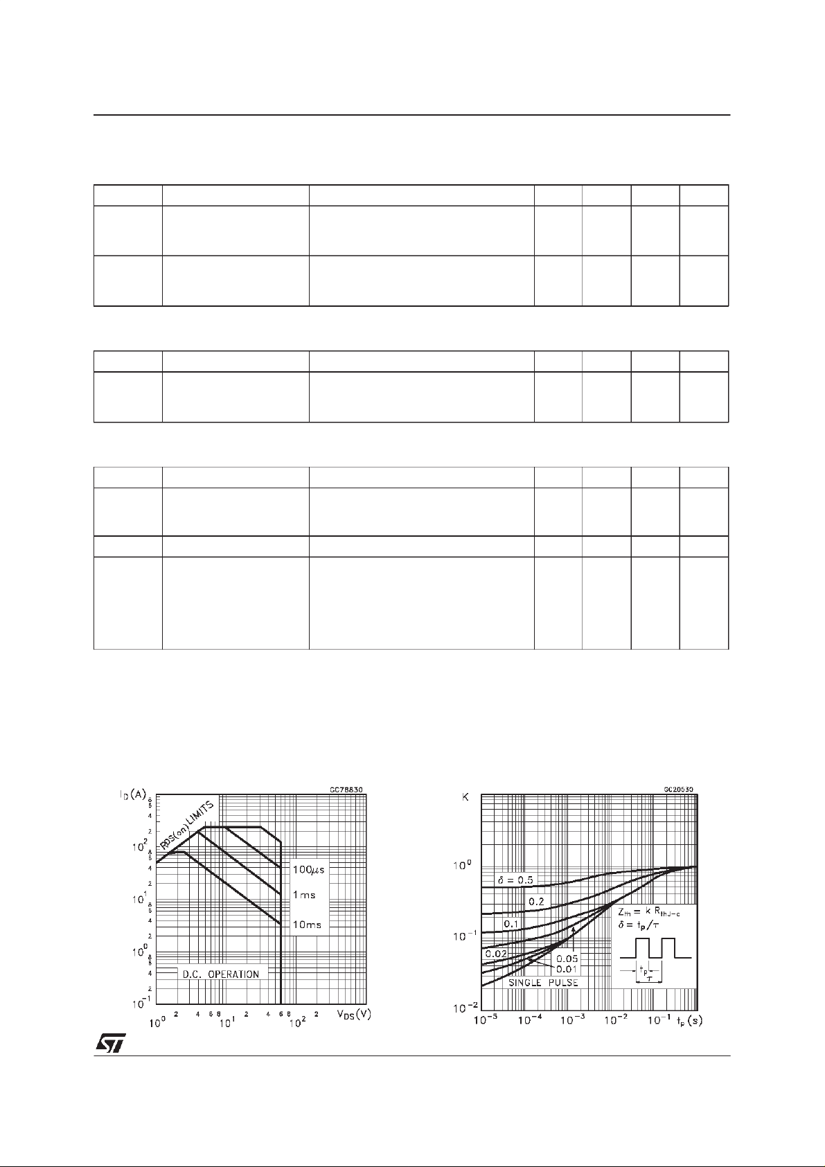
Safe Operating Area ThermalImpedance
3/8
Page 4

STW80NE06-10
OutputCharacteristics
Transconductance
TransferCharacteristics
StaticDrain-sourceOn Resistance
GateCharge vs Gate-sourceVoltage
4/8
CapacitanceVariations
Page 5

STW80NE06-10
Normalized GateThresholdVoltage vs
Temperature
Source-drainDiode Forward Characteristics
Normalized On Resistancevs Temperature
5/8
Page 6

STW80NE06-10
Fig. 1: UnclampedInductive Load Test Circuit
Fig. 3: SwitchingTimes Test Circuits For
ResistiveLoad
Fig. 2: Unclamped Inductive Waveform
Fig. 4: GateCharge testCircuit
Fig. 5: Test Circuit For InductiveLoad Switching
And Diode RecoveryTimes
6/8
Page 7

TO-247 MECHANICAL DATA
STW80NE06-10
DIM.
MIN. TYP. MAX. MIN. TYP. MAX.
A 4.7 5.3 0.185 0.209
D 2.2 2.6 0.087 0.102
E 0.4 0.8 0.016 0.031
F 1 1.4 0.039 0.055
F3 2 2.4 0.079 0.094
F4 3 3.4 0.118 0.134
G 10.9 0.429
H 15.3 15.9 0.602 0.626
L 19.7 20.3 0.776 0.779
L3 14.2 14.8 0.559 0.413 0.582
L4 34.6 1.362
L5 5.5 0.217
M 2 3 0.079 0.118
Dia 3.55 3.65 0.140 0.144
mm inch
P025P
7/8
Page 8

STW80NE06-10
Information furnished is believed tobe accurate and reliable. However, STMicroelectronics assumes no responsibility for the consequences
of use of such information nor for any infringement of patents or other rights of third parties which may resultfrom its use. No license is
granted by implication orotherwiseunder any patent or patent rights of STMicroelectronics. Specification mentioned in this publication are
subject tochange without notice. This publication supersedes and replaces allinformation previouslysupplied. STMicroelectronics products
are not authorized for use as critical componentsin life support devices or systems without express written approval of STMicroelectronics.
Australia - Brazil - Canada - China - France- Germany - Italy - Japan- Korea - Malaysia -Malta - Mexico - Morocco- The Netherlands -
Singapore- Spain- Sweden- Switzerland- Taiwan -Thailand - United Kingdom- U.S.A.
The ST logo isa trademarkof STMicroelectronics
1998 STMicroelectronics– Printed in Italy – All Rights Reserved
STMicroelectronicsGROUP OFCOMPANIES
.
8/8
 Loading...