

Page 1
STW7NC90Z
N-CHANNEL 900V - 1.55Ω - 6A TO-247
Zener-Protected PowerMESH™III MOSFET
TYPE V
DSS
STW7NC90Z 900 V < 1.9
■ TYPICAL R
■ EXTREMELY HIGH dv /d t CAPABILITY
■ GATE-TO-SOURCE ZENER DIODES
■ 100% AVALANCHE TESTED
■ VERY LOW INTRINSIC CAPAC ITANCES
■ GATE CHARGE MINIMIZED
(on) = 1.55Ω
DS
R
DS(on)
I
D
Ω
6 A
DESCRIPTION
The third generation of MESH O VERLAY™ Power
MOSFETs for very high voltage exhibits unsurpassed on-resistance per unit area while integrating
back-to-back Zener diodes between gate and
source. Such arrangement gives extra ESD capability with higher ruggedness performance as requested by a large variety of single-switch applications.
APPLICATIONS
■ SINGLE-ENDED SMPS IN MONITORS,
COMPUTER AND INDUSTRIAL APPLICATION
■ WELDING EQUIPMENT
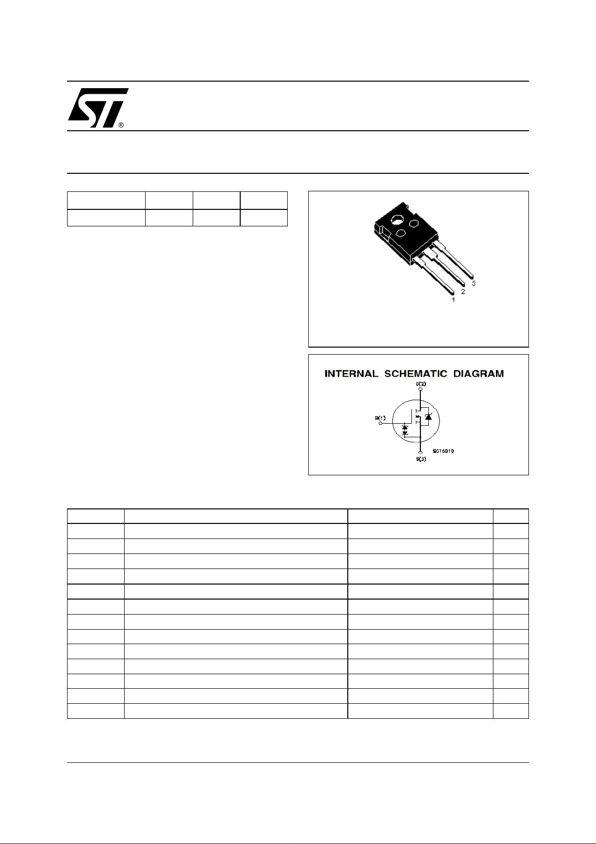
TO-247
ABSOLUTE MAXIMUM RATINGS
Symbol Parameter Value Unit
V
DS
V
DGR
V
GS
I
D
I
D
I
DM
P
TOT
I
GS
V
ESD(G-S)
dv/dt(1) Peak Diode Recovery voltage slope 3 V/ns
T
stg
T
j
(•)Pu l se width limite d by safe operat i ng area
≤6A, di/dt ≤100A/µs, VDD ≤ V
(1)I
SD
Drain-source Voltage (VGS = 0)
Drain-gate Voltage (RGS = 20 kΩ)
900 V
900 V
Gate- source Voltage ±25 V
Drain Current (continuos) at TC = 25°C
Drain Current (continuos) at TC = 100°C
(●)
Drain Current (pulsed) 24 A
Total Dissipation at TC = 25°C
6A
3.8 A
160 W
Derating Factor 1.28 W/°C
Gate-source Current (DC) ±50 mA
Gate source ESD(HBM-C=100pF, R=15K
Ω)
3KV
Storage Temperature –65 to 150 °C
Max. Operating Junction Temperature 150 °C
(*) Limited by maximum temperature allowed
, Tj ≤ T
(BR)DSS
JMAX.
1/8May 2001
Page 2
STW7NC90Z
THERMA L D ATA
Rthj-case Thermal Resistance Junction-case Max 0.78 °C/W
Rthj-amb Thermal Resistance Junction-ambient Max 30 °C/W
T
l
AVALANCHE CHARACTERISTICS
Symbol Parameter Max Value Unit
I
AR
E
AS
ELECTRICAL CHARACTERISTICS (TCASE = 25 °C UNLESS OTHERWISE SPECIFIED)
OFF
Symbol Parameter Test Conditions Min. Typ. Max. Unit
V
(BR)DSS
∆
BV
DSS
I
DSS
I
GSS
Maximum Lead Temperature For Soldering Purpose 300 °C
Avalanche Current, Repetitive or Not-Repetitive
(pulse width limited by T
max)
j
Single Pulse Avalanche Energy
(starting T
Drain-source
= 25 °C, ID = IAR, VDD = 50 V)
j
ID = 250 µA, VGS = 0 900 V
6A
315 mJ
Breakdown Voltage
/∆TJBreakdown Voltage Temp.
ID = 1 mA, VGS = 0 1 V/°C
Coefficient
Zero Gate Voltage
Drain Current (V
GS
Gate-body Leakage
Current (V
DS
= 0)
= 0)
V
= Max Rating
DS
V
= Max Rating, TC = 125 °C
DS
V
= ±20V ±10 µA
GS
1µA
50 µA
ON
(1)
Symbol Parameter Test Conditions Min. Typ. Max. Unit
V
V
GS(th)
R
DS(on)
Gate Threshold Voltage
Static Drain-source On
= VGS, ID = 250µA
DS
VGS = 10V, ID = 3A
345V
1.55 1.9
Resistance
DYNAMIC
Symbol Parameter Test Conditions Min. Typ. Max. Unit
(1) Forward Transconductance VDS > I
g
fs
C
iss
C
oss
C
rss
Input Capacitance
Output Capacitance 150 pF
Reverse Transfer
Capacitance
ID=3A
V
DS
D(on)
x R
DS(on)max,
= 25V, f = 1 MHz, VGS = 0
5.7 S
2290 pF
15 pF
Ω
2/8
Page 3
STW7NC90Z
ELECTRICAL CHARACTERISTICS (CONTINUED)
SWITCHING ON (RESISTIVE LOAD)
Symbol Parameter Test Conditions Min. Typ. Max. Unit
V
t
d(on)
Q
Q
Q
t
r
gs
gd
Turn-on Delay Time
Rise Time 12 ns
Total Gate Charge
g
Gate-Source Charge 13 nC
Gate-Drain Charge 15 nC
SWITCHING OFF (INDUCTIVE LOAD)
Symbol Parameter Test Conditions Min. Typ. Max. Unit
t
r(Voff)
t
t
f
c
Off-voltage Rise Time
Fall Time 11 ns
Cross-over Time 14 ns
SOURCE DRAIN DIODE
Symbol Parameter Test Conditions Min. Typ. Max. Unit
I
SD
I
SDM
VSD (1)
t
rr
Q
I
RRM
Source-drain Current 6 A
(2)
Source-drain Current (pulsed) 24 A
Forward On Voltage
Reverse Recovery Time
Reverse Recovery Charge 7.14 µC
rr
Reverse Recovery Current 21 A
= 450V, ID = 3A
DD
RG= 4.7Ω VGS = 10V
(see test circuit, Figure 3)
V
= 720V, ID = 6 A,
DD
VGS = 10V
V
= 720V, ID = 6 A,
DD
RG=4.7Ω, V
GS
= 10V
(see test circuit, Figure 5)
ISD = 6 A, VGS = 0
I
= 6 A, di/dt = 100A/µs,
SD
VDD = 40 V, Tj = 150°C
(see test circuit, Figure 5)
30 ns
42 58.8 nC
10 ns
1.6 V
680 ns
GATE-SOURCE ZENER DIODE
Symbol Parameter Test Conditions Min. Typ. Max. Unit
BV
GSO
Gate-Source Breakdown
Igs=± 1mA (Open Drain) 25 V
Voltage
α
T Voltage Thermal Coefficient T=25°C Note(3) 1.3
I
Rz Dynamic Resistance
Note: 1. Pulsed: Pu l se duration = 300 µs, duty cycle 1.5 %.
2. Pulse width li mited by safe operating area.
3. ∆
= αT (25°-T) BV
V
BV
GSO
(25°)
= 50 mA
GS
90
10
-4
/°C
Ω
PROTECTION FEATURES OF GATE-TO-SOURCE ZENER DIODES
The built-in back-to-back Zener diodes have specif ically been designed to enhanc e not only t he dev ice’s
ESD capability, but also to make them safely absorb possible voltage transients that may occasionally be
applied from gate to souce. In this respect the 25V Zener voltage is appropiate to achieve an efficient and
cost-effective intervention to protect the device’s integrity. These integrated Zener diode s thus avoi d t he
usage of external components.
3/8
Page 4

STW7NC90Z
Thermal ImpedanceSafe Operating Area
Output Characteristics
Transfer Characteristics
Static Drain-source On ResistanceTransconductance
4/8
Page 5

STW7NC90Z
Gate Charge vs Gate-source Voltage Capacitance Variations
Normalized Gate Threshold Volta ge vs Temp. Normalized On Resistance vs Temp eratur e
Source-drain Diode Forward Characteristics
5/8
Page 6
STW7NC90Z
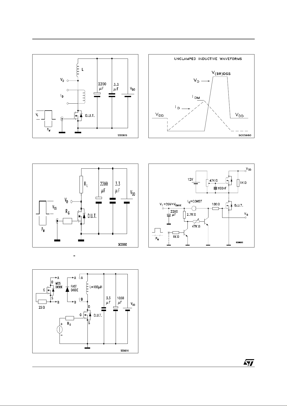
Fig. 2: Unclamped Inductive WaveformFig. 1: Unclamped Inductive Load Test Circuit
Fig. 3: Switching Times Test Circuit For
Resistive Load
Fig. 5: Test Circuit For Inductive Load Switching
And Diode Recovery Times
Fig. 4: Gate Charge test Circuit
6/8
Page 7

TO-247 MECHANICAL DATA
STW7NC90Z
DIM.
A 4.85 5.15 0.19 0.20
D 2.20 2.60 0.08 0.10
E 0.40 0.80 0.015 0.03
F 1 1.40 0.04 0.05
F1 3 0.11
F2 2 0.07
F3 2 2.40 0.07 0.09
F4 3 3.40 0.11 0.13
G 10.90 0.43
H 15.45 15.75 0.60 0.62
L 19.85 20.15 0.78 0.79
L1 3.70 4.30 0.14 0.17
L2 18.50 0.72
L3 14.20 14.80 0.56 0.58
L4 34.60 1.36
L5 5.50 0.21
M 2 3 0.07 0.11
V
V2
Dia 3.55 3.65 0.14 0.143
MIN. TYP MAX. MIN. TYP. MAX.
mm. inch
5º5º
60º 60º
7/8
Page 8

STW7NC90Z
8/8
Information furnished is believed to be accurate and reliable. However, STMicroelectronics assumes no responsibility for the consequences
of use of such informa tion n or for an y infring ement of patent s or other rig hts of third part ies which may resu lt from its use . No l i cen se i s
granted by implication or otherwise under any patent or patent rights of STMicroelectronics. Specification mentioned in this publication are
subject to change without notice. This publication supersedes and replaces all information previously supplied. STMicroelectronics products
are not authorized for use as critical compo nents in life support devices or systems without express written approval of STMicroelectronics.
Australia - Brazil - China - Finland - France - Germany - Hong Kong - India - Italy - Japan - Malaysia - Malta - Morocco -
The ST logo is a trademark of STMicroelectronics
© 2001 STMicroelectronics – Printed in Italy – All Rights Reserved
STMicroelectronics GROUP OF COMPANIES
Singapore - Spain - Sweden - Switzerland - United Kingdom - U.S.A.
http://www.st.com
 Loading...