

Page 1
STW7NB80
N-CHANNEL 800V - 1.6Ω - 6.5A - TO-247
PowerMESH MOSFET
TYPE V
DSS
R
DS(on)
I
D
ST W7NB80 800 V < 1. 9 Ω 6.5 A
■ TYPICALR
■ EXTREMELY HIGH dv/dt CAPABILITY
■ ± 30VGATETO SOURCEVOLTAGERATING
■ 100%AVALANCHETESTED
■ VERYLOW INTRINSIC CAPACITANCES
■ GATECHARGE MINIMIZED
DS(on)
= 1.6 Ω
DESCRIPTION
Using the latesthigh voltage MESH OVERLAY
process, STMicroelectronics has designed an
advanced family of power MOSFETs with
outstanding performances. The new patent
pending strip layout coupled with the Company’s
proprietary edge termination structure, gives the
lowest RDS(on) per area, exceptional avalanche
and dv/dt capabilities and unrivalled gate charge
and switching characteristics.
APPLICATIONS
■ HIGHCURRENT, HIGH SPEEDSWITCHING
■ SWITCHMODE POWER SUPPLIES (SMPS)
■ DC-AC CONVERTERS FORWELDING
EQUIPMENTANDUNINTERRUPTIBLE
POWERSUPPLIESAND MOTOR DRIVE
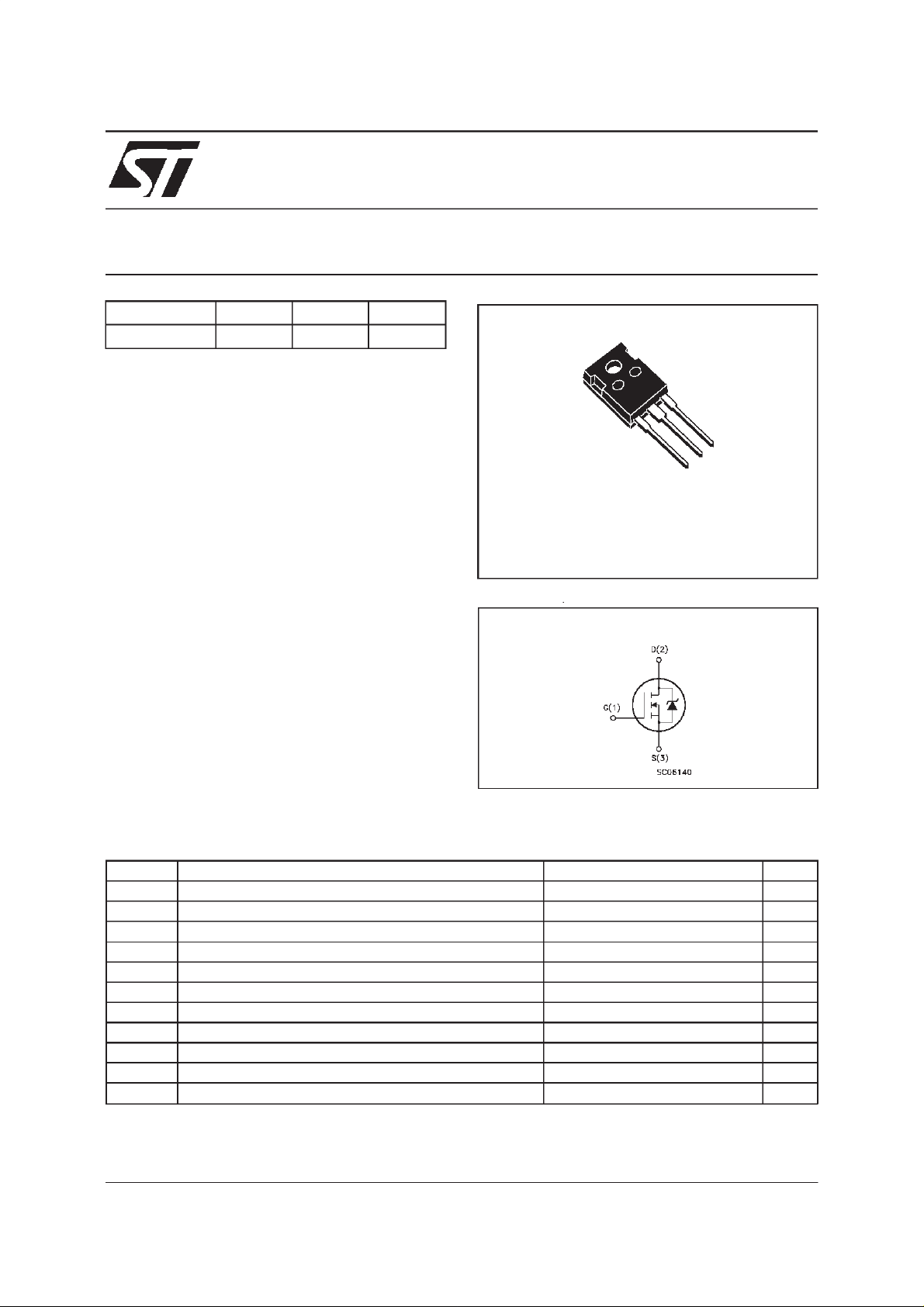
3
2
1
TO-247
INTERNAL SCHEMATIC DIAGRAM
ABSOLUTE MAXIMUM RATINGS
Symbol Parameter Value Unit
V
V
V
I
DM
P
dv/dt(
T
(•) Pulsewidth limitedby safeoperating area (1) I
December 1999
Dra in- sour c e Volt age (VGS= 0) 800 V
DS
Dra in- gat e V ol t age (RGS=20kΩ)
DGR
Gat e-source Voltage
GS
Dra in Cu rr ent (contin uous ) a t Tc=25oC6.5A
I
D
Dra in Cu rr ent (contin uous ) a t Tc=100oC4.1A
I
D
800 V
30 V
±
(•) Dra in Cu rr ent (pulsed) 26 A
Tot al Dis sipation at Tc=25oC 160 W
tot
Der ati ng Fac t or 1.28 W/
1) Peak Di ode Re covery voltage sl ope 4 V/ns
St orage T em pe r at ur e -65 to 150
stg
Max. Operating Junc tion T emperat ure 150
T
j
≤
6 A, di/dt≤200A/µs, V
SD
≤
DD
V
(BR)DSS
,Tj≤T
JMAX
o
C
o
C
o
C
1/8
Page 2
STW7NB80
THERMAL DATA
R
thj-case
R
thj-amb
R
thc-sink
T
AVALANCHE CHARACTERISTICS
Symbol Parameter Max V alue Unit
I
AR
E
Ther mal Res istance Junct ion-case Max 0.78
Ther mal Res istance Junct ion-ambient Max
Ther mal Res istance C as e -s ink Ty p
Maximum L ead Te mperature For Soldering Pur p os e
l
Avalanche C urrent, R epetitive or Not-Repetitive
(pulse width limited by T
Single Pul se Avalanche Energy
AS
(starting T
=25oC, ID=IAR,VDD=50V)
j
max)
j
30
0.1
300
6.5 A
260 mJ
o
C/W
o
C/W
o
C/W
o
C
ELECTRICAL CHARACTERISTICS (T
=25oC unless otherwisespecified)
case
OFF
Symbol Parameter Test Con ditions Min. Typ. Max. Unit
V
(BR)DSS
Drain-source
=250µAVGS=0
I
D
800 V
Break dow n Vo lt age
I
DSS
I
GSS
Zero Gate Voltage
Drain Curre nt (V
GS
Gat e- bod y Leakage
Current (V
DS
=0)
=0)
V
=MaxRating
DS
=MaxRating Tc= 125oC
V
DS
= ± 30 V
V
GS
1
50
± 100 nA
ON(∗)
Symbol Parameter Test Con ditions Min. Typ. Max. Unit
V
GS(th)
R
DS(on)
Gate Threshold Voltage
Sta t ic Drain-s ource On
V
DS=VGSID
= 250 µA
VGS=10V ID=3A 1.6 1.9
345V
Resistance
I
D(on)
On State Drain Current VDS>I
D(on)xRDS(on)max
6.5 A
VGS=10V
DYNAMIC
Symbol Parameter Test Con ditions Min. Typ. Max. Unit
g
(∗)Forward
fs
Tr ansc on duc tance
C
C
C
Input Capacit anc e
iss
Out put Capac it ance
oss
Reverse Transfer
rss
Capacit a nc e
VDS>I
D(on)xRDS(on)maxID
=3A 2.5 4.7 S
VDS=25V f=1MHz VGS= 0 1250
145
16
µA
µ
Ω
Ω
pF
pF
pF
A
2/8
Page 3
STW7NB80
ELECTRICAL CHARACTERISTICS
(continued)
SWITCHING ON
Symbol Parameter Test Con ditions Min. Typ. Max. Unit
t
d(on)
Q
Q
Q
Turn-on Time
t
Rise T ime
r
Tot al Gate Charge
g
Gat e- Source Charge
gs
Gate-Drain Charge
gd
VDD=400V ID=3A
R
=4.7
G
Ω
VGS=10V
VDD= 640 V ID=6A VGS=10V
R
=4.7
G
Ω
VGS=10V
19
33
11
14
9
47 nC
SWITCHING OFF
Symbol Parameter Test Con ditions Min. Typ. Max. Unit
t
r(Voff)
t
t
Off-voltage Rise Tim e
Fall T ime
f
Cross-over Time
c
VDD=640V ID=6A
=4.7 ΩVGS=10V
R
G
11
9
16
SOURCEDRAINDIODE
Symbol Parameter Test Con ditions Min. Typ. Max. Unit
I
SD
I
SDM
V
SD
t
Q
I
RRM
(∗) Pulsed:Pulse duration= 300µs, dutycycle 1.5 %
(•) Pulse width limited by safeoperating area
Source-drain Current
(•)
Source-drain Current
6.5
26
(pulsed)
(∗)ForwardOnVoltage ISD=6A VGS=0 1.6 V
Reverse Recovery
rr
Time
Reverse Recovery
rr
=6A di/dt=100A/µs
I
SD
= 100 V Tj=150oC
V
DD
700
5.8
Charge
Reverse Recovery
16.5
Current
ns
ns
nC
nC
ns
ns
ns
A
A
ns
µ
A
C
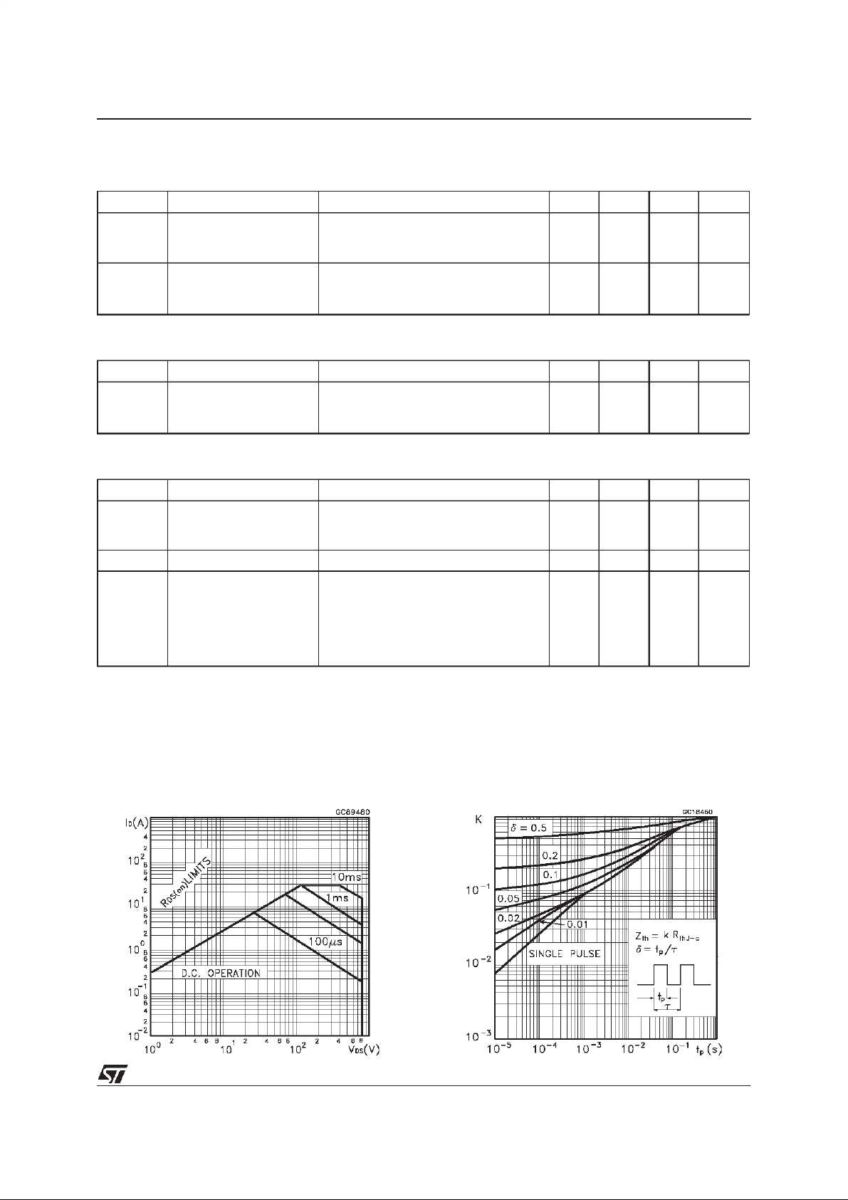
SafeOperating Area ThermalImpedance
3/8
Page 4

STW7NB80
OutputCharacteristics
Transconductance
TransferCharacteristics
Static Drain-sourceOn Resistance
Gate Charge vs Gate-sourceVoltage
4/8
CapacitanceVariations
Page 5

STW7NB80
NormalizedGate ThresholdVoltage vs
Temperature
Source-drainDiode Forward Characteristics
NormalizedOn Resistancevs Temperature
5/8
Page 6

STW7NB80
Fig. 1: UnclampedInductiveLoad Test Circuit
Fig. 3: SwitchingTimesTest CircuitsFor
ResistiveLoad
Fig. 2:UnclampedInductive Waveform
Fig. 4: Gate Charge test Circuit
Fig. 5: TestCircuit ForInductiveLoad Switching
And Diode Recovery Times
6/8
Page 7

TO-247 MECHANICAL DATA
STW7NB80
DIM.
MIN. TYP. MAX. MIN. TYP. MAX.
A 4.7 5.3 0.185 0.209
D 2.2 2.6 0.087 0.102
E 0.4 0.8 0.016 0.031
F 1 1.4 0.039 0.055
F3 2 2.4 0.079 0.094
F4 3 3.4 0.118 0.134
G 10.9 0.429
H 15.3 15.9 0.602 0.626
L 19.7 20.3 0.776 0.779
L3 14.2 14.8 0.559 0.582
L4 34.6 1.362
L5 5.5 0.217
M 2 3 0.079 0.118
mm inch
P025P
7/8
Page 8

STW7NB80
Information furnished is believed tobeaccurateand reliable.However, STMicroelectronics assumes no responsibility forthe consequences
of use of such information nor for any infringement of patents or other rights of third parties which may result from its use. No license is
granted by implication or otherwise under any patent or patent rights of STMicroelectronics. Specificationmentioned in thispublication are
subjecttochange without notice. This publicationsupersedesandreplaces all information previouslysupplied.STMicroelectronics products
are not authorized for use as critical components in lifesupport devices or systemswithout express written approval of STMicroelectronics.
The STlogo is a trademark ofSTMicroelectronics
1999STMicroelectronics – Printedin Italy – All RightsReserved
STMicroelectronics GROUP OF COMPANIES
Australia - Brazil - China- Finland - France - Germany - Hong Kong - India - Italy - Japan - Malaysia- Malta - Morocco -
8/8
Singapore - Spain - Sweden - Switzerland - United Kingdom- U.S.A.
http://www.st.com
.
 Loading...