

Page 1
STW6NB100
N - CHANNEL 1000V - 2.3Ω - 5.4A - TO-247
PowerMESH MOSFET
TYPE V
DSS
R
DS(on)
I
D
STW6NB100 1000 V < 2.8 Ω 5.4 A
■ TYPICALR
■ EXTREMELYHIGH dv/dt CAPABILITY
■ ± 30VGATETO SOURCEVOLTAGERATING
■ 100%AVALANCHETESTED
■ VERYLOW INTRINSIC CAPACITANCES
■ GATECHARGE MINIMIZED
DS(on)
= 2.3 Ω
DESCRIPTION
Using the latest high voltage technology,
STMicroelectronics has designed an advanced
family of power Mosfets with outstanding
performances. The new patent pending strip
layout coupled with the Company’s proprietary
edge termination structure, gives the lowest
R
(on) per area, exceptional avalanche and
DS
dv/dt capabilities and unrivalled gate charge and
switchingcharacteristics.
APPLICATIONS
■ HIGHCURRENT, HIGH SPEEDSWITCHING
■ SWITCHMODE POWER SUPPLIES(SMPS)
■ DC-AC CONVERTERS FORWELDING
EQUIPMENTAND UNINTERRUPTIBLE
POWERSUPPLIESAND MOTOR DRIVE
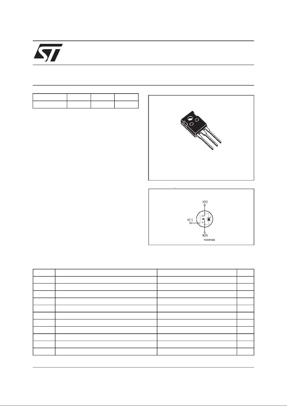
3
2
1
TO-247
INTERNAL SCHEMATIC DIAGRAM
ABSOLUTE MAXIMUM RATINGS
Symbol Parameter Value Unit
V
V
V
I
DM
P
dv/dt(
T
(•) Pulsewidth limited by safeoperating area ( 1)ISD≤ 5.4 A, di/dt ≤ 200 A/µs, VDD≤ V
October 1999
Drain-source Voltage (VGS= 0) 1000 V
DS
Drain- gate Voltage (RGS=20kΩ)
DGR
Gat e-sourc e Volt ag e ± 30 V
GS
I
Drain Cu r re nt (continuous) at Tc=25oC 5.4 A
D
I
Drain Cu r re nt (continuous) at Tc= 100oC 3.4 A
D
1000 V
(•) Drain Current (pulsed) 21 A
Tot al Dissipation at Tc=25oC160W
tot
Dera ti ng Fact or 1.28 W/
1) Peak Diode Recovery volta ge sl ope 4 V/ ns
Sto rage Temperat u r e -65 t o 15 0
stg
T
Max. Oper ating Junction Temperature 150
j
,Tj≤T
(BR)DSS
JMAX
o
C
o
C
o
C
1/8
Page 2
STW6NB100
THERMAL DATA
R
thj-case
R
thj-amb
R
thc-sink
T
AVALANCHE CHARACTERISTICS
Symbol Para meter Max V al ue Uni t
I
AR
E
Ther mal Resis t an c e Juncti on-case Max
Ther mal Resis t an c e Juncti on-ambien t Max
Thermal Resistance Case-sink Typ
Maximum Lead Temperature Fo r Soldering Purpose
l
Avalanche Current, Re petitive or No t -Repetit ive
(pulse width limited by T
Single Pulse Avalanche Energy
AS
(starting T
=25oC, ID=IAR,VDD=50V)
j
max)
j
0.78
62.5
0.5
300
5.4 A
373 mJ
o
C/W
oC/W
o
C/W
o
C
ELECTRICAL CHARACTERISTICS (T
=25oC unless otherwisespecified)
case
OFF
Symbol Parameter Test Conditions Min. Typ. Max. Unit
V
(BR)DSS
Drain-source
=250µAVGS=0
I
D
1000 V
Break d own Voltage
I
DSS
I
GSS
Zero Gate Voltage
Drain Cu rr ent (V
GS
Gat e- b ody Leak a ge
Current ( V
DS
=0)
=0)
V
=MaxRating
DS
= Max Rating Tc=125oC
V
DS
= ± 30 V
V
GS
1
50
± 100 nA
ON(∗)
Symbol Parameter Test Conditions Min. Typ. Max. Unit
V
GS(th)
Gate Threshold
V
DS=VGSID
= 250 µA
345V
Voltage
R
DS(on)
Static Drain-source On
VGS=10V ID= 2.7 A 2.5 2.8
Resistance
I
D(on)
On S t ate Drain Current VDS>I
D(on)xRDS(on )max
6A
VGS=10V
DYNAMIC
Symbol Parameter Test Conditions Min. Typ. Max. Unit
g
(∗)Forward
fs
Tr ansconductance
C
C
C
Input Cap acitance
iss
Out put Capac it ance
oss
Reverse Transfer
rss
Capacitance
VDS>I
D(on)xRDS(on )maxID
=2.7A 1.5 3 S
VDS=25V f=1MHz VGS= 0 1500
180
17
µA
µ
Ω
pF
pF
pF
A
2/8
Page 3
STW6NB100
ELECTRICAL CHARACTERISTICS
(continued)
SWITCHING ON
Symbol Parameter Test Conditions Min. Typ. Max. Unit
t
d(on)
t
r
Turn-on Time
Rise Time
VDD= 500 V ID=2.5A
R
=4.7
G
Ω
VGS=10V
24
11
(see test circu it, figure 3)
Q
Q
Q
Total Gate Charge
g
Gat e- Source Charge
gs
Gate-Drain Charge
gd
VDD= 800 V ID=5A VGS=10V 39
10
19
55 nC
SWITCHING OFF
Symbol Parameter Test Conditions Min. Typ. Max. Unit
t
r(Voff)
t
t
Off -voltage Rise Ti me
Fall Time
f
Cross-over Time
c
VDD= 800 V ID=5A
=4.7 ΩVGS=10V
R
G
(see test circu it, figure 5)
40
22
26
SOURCEDRAINDIODE
Symbol Parameter Test Conditions Min. Typ. Max. Unit
I
SD
I
SDM
V
SD
t
Q
I
RRM
(∗) Pulsed: Pulse duration = 300µs, duty cycle 1.5%
(•) Pulse width limited by safeoperating area
Source-drain Curr ent
(•)
Source-drain Curr ent
5.4
21
(pulsed)
(∗) Forward O n Voltage ISD=5.4A VGS=0 1.6 V
Reverse R ec o v ery
rr
Time
Reverse R ec o v ery
rr
= 5 A d i/ d t = 100 A/µs
I
SD
= 100 V Tj=150oC
V
DD
(see test circu it, figure 5)
780
5.5
Charge
Reverse R ec o v ery
14
Current
ns
ns
nC
nC
ns
ns
ns
A
A
ns
µ
A
C
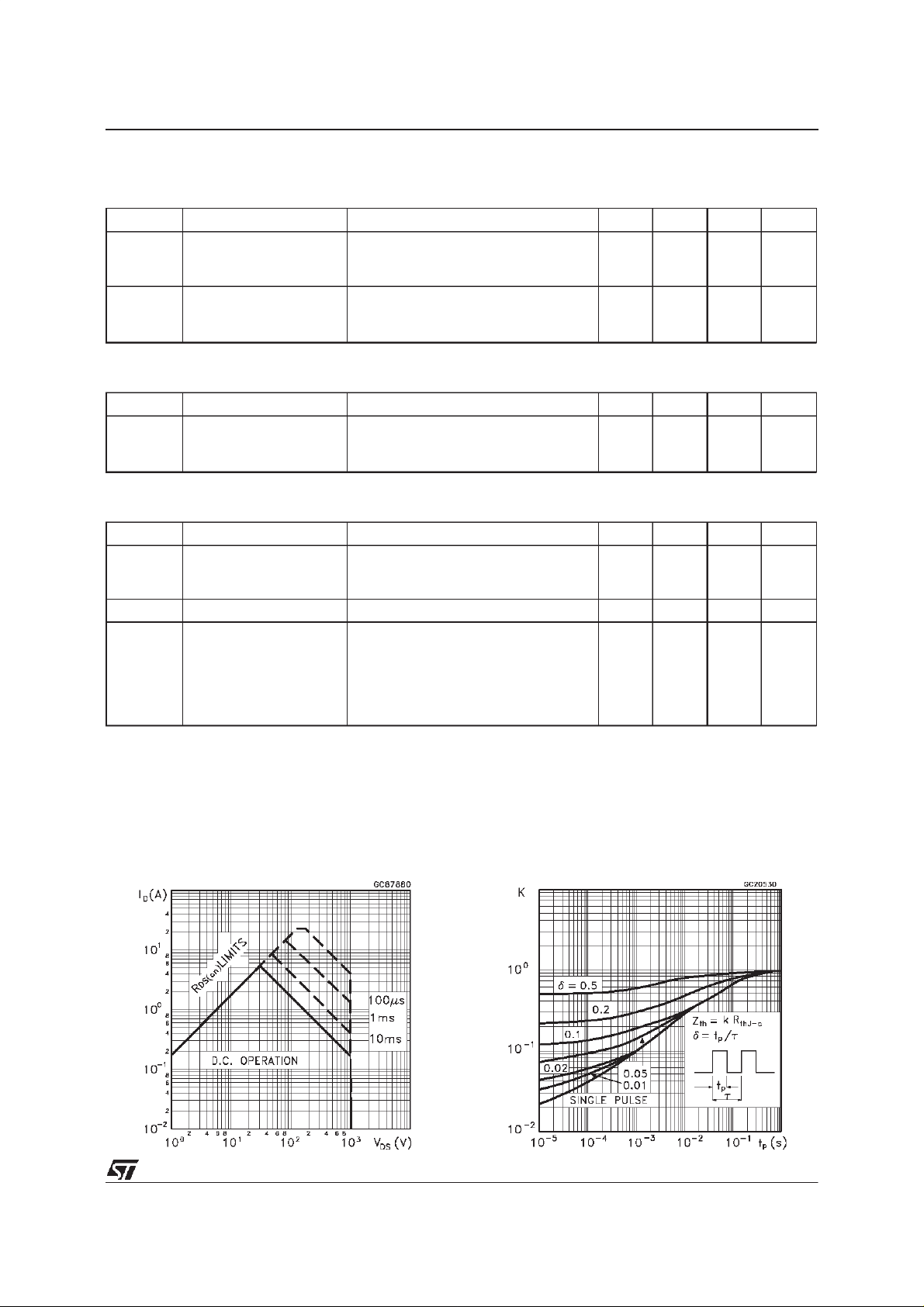
SafeOperating Area Thermal Impedance
3/8
Page 4

STW6NB100
OutputCharacteristics
Transconductance
TransferCharacteristics
Static Drain-sourceOn Resistance
Gate Charge vs Gate-sourceVoltage
4/8
CapacitanceVariations
Page 5

STW6NB100
Normalized GateThreshold Voltagevs
Temperature
Source-drainDiode Forward Characteristics
Normalized On Resistance vs Temperature
5/8
Page 6

STW6NB100
Fig. 1:
UnclampedInductive LoadTest Circuit
Fig. 3: SwitchingTimes Test CircuitsFor
ResistiveLoad
Fig. 2:
UnclampedInductiveWaveform
Fig. 4: Gate Charge test Circuit
Fig. 5:
Test Circuit For InductiveLoad Switching
And Diode Recovery Times
6/8
Page 7

TO-247 MECHANICAL DATA
STW6NB100
DIM.
MIN. TYP. MAX. MIN. TYP. MAX.
A 4.7 5.3 0.185 0.209
D 2.2 2.6 0.087 0.102
E 0.4 0.8 0.016 0.031
F 1 1.4 0.039 0.055
F3 2 2.4 0.079 0.094
F4 3 3.4 0.118 0.134
G 10.9 0.429
H 15.3 15.9 0.602 0.626
L 19.7 20.3 0.776 0.779
L3 14.2 14.8 0.559 0.582
L4 34.6 1.362
L5 5.5 0.217
M 2 3 0.079 0.118
mm inch
P025P
7/8
Page 8

STW6NB100
Information furnished is believed to beaccurateand reliable. However, STMicroelectronics assumes no responsibilityfor the consequences
of use of such information nor for any infringement of patents or other rights of third parties which may result from its use. No license is
granted by implication or otherwise under anypatent or patent rights of STMicroelectronics. Specificationmentioned in thispublicationare
subjecttochange without notice. Thispublication supersedes and replaces all information previously supplied.STMicroelectronics products
are not authorized for use as critical components in lifesupport devicesor systemswithout express written approval of STMicroelectronics.
The STlogo is a trademark of STMicroelectronics
1999STMicroelectronics – Printed in Italy– All Rights Reserved
STMicroelectronics GROUP OF COMPANIES
Australia - Brazil - China- Finland- France - Germany -Hong Kong - India - Italy - Japan- Malaysia - Malta - Morocco -
8/8
Singapore - Spain - Sweden - Switzerland - United Kingdom- U.S.A.
http://www.st.com
.
 Loading...