

Page 1
STW6NA80
STH6NA80FI
N - CHANNEL 800V - 1.8Ω - 5.4A - TO-247/ISOWATT218
FAST POWER MOS TRANSISTOR
TYPE V
STW6NA80
ST H6 NA80FI
■ TYPICALR
■ AVALANCERUGGED TECHNOLOGY
■ 100%AVALANCHETESTED
■ REPETITIVEAVALANCHEDATA AT 100
■ LOW GATE CHARGE
■ VERYHIGH CURRENTCAPABILITY
■ APPLICATIONORIENTED
DS(on)
DSS
800 V
800 V
= 1.8
CHARACTERIZATION
APPLICATIONS
■ HIGHCURRENT, HIGH SPEED SWITCHING
■ SOLENOIDAND RELAY DRIVERS
■ REGULATORS
■ DC-DC& DC-ACCONVERTERS
■ MOTORCONTROL, AUDIO AMPLIFIERS
■ AUTOMOTIVEENVIRONMENT (INJECTION,
ABS, AIR-BAG, LAMPDRIVERS,Etc.)
Ω
R
DS(on)
<2.2Ω
<2.2
Ω
I
D
5.4 A
3.4 A
o
C
3
2
1
1
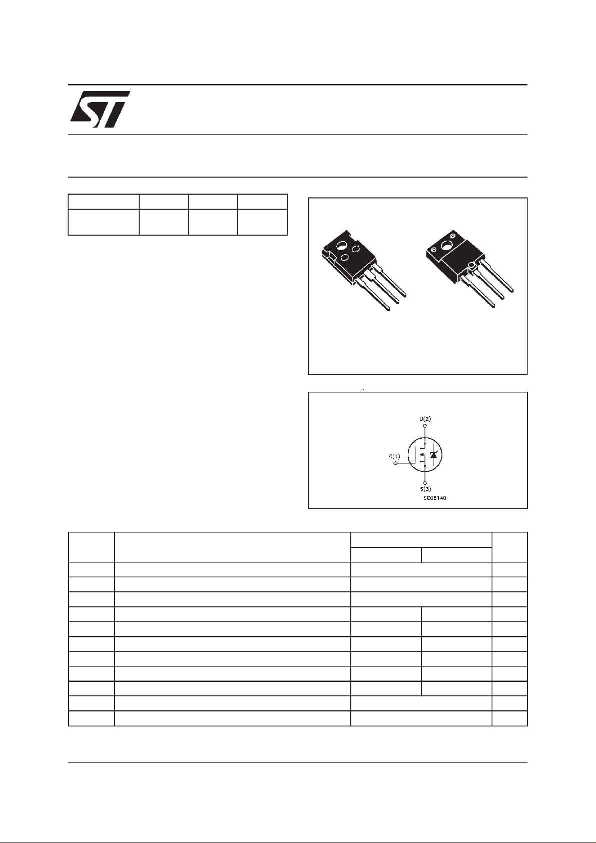
TO-247 ISOWATT218
INTERNAL SCHEMATIC DIAGRAM
3
2
ABSOLUTE MAXIMUM RATINGS
Symbol Parameter Value Unit
ST W 6N A80 STH 6NA 80FI
V
V
V
I
DM
P
V
T
(•) Pulsewidth limited by safeoperating area
October 1998
Drain-source Voltage (VGS=0) 800 V
DS
Dra in- gat e Voltage (RGS=20kΩ)
DGR
Gate -sourc e Vo ltage ± 30 V
GS
I
Drain Current (co ntinuous) at Tc=25oC5.4
D
I
Drain Current (co ntinuous) at Tc=100oC3.4
D
800 V
(•) Drain Current (pulsed) 22
Total Dissipation at Tc=25oC 150
tot
Derating Factor 1.2
Insulat ion Withstand Vo ltage (DC ) 4000 V
ISO
St orage Temperature -65 t o 1 50
stg
T
Max. Op er a t ing J unction Tem pe rat ure 150
j
3.4
2.1
22
60
0.48
W/
A
A
A
W
o
o
o
C
C
C
1/10
Page 2
STW6NA80-STH6NA80FI
THERMAL DATA
TO-247 ISOWAT T 218
R
thj-case
R
thj-amb
R
thc-sink
T
AVALANCHE CHARACTERISTICS
Symbol Para meter Max V al ue Uni t
I
AR
E
E
I
AR
Ther mal Resist ance Junction- case Max 0.83 2.08
Ther mal Resist ance Junction- amb ient Max
Thermal Resistance Case-sink Typ
Maximum Lead Tem perature For Soldering P urpose
l
Avalanche Curr ent, Re petitive or No t -Repetit ive
(pulse width limited by T
Single Pulse Avalanche Energ y
AS
(starting T
Repetitive Avalanche Energy
AR
=25oC, ID=IAR,VDD=50V)
j
(pulse width limited by T
max, δ <1%)
j
max,δ <1%)
j
Avalanche Curr ent, Re petitive or No t -Repetit ive
= 100oC, pulse widt h limit ed by Tjmax, δ <1%)
(T
c
30
0.1
300
5.4 A
150 mJ
5.8 mJ
3.4 A
o
C/W
o
C/W
o
C/W
o
C
ELECTRICAL CHARACTERISTICS
=25oC unless otherwisespecified)
(T
case
OFF
Symbol Parameter Test Condit ions Min. Typ. Max. Unit
V
(BR)DSS
Drain-source
=250µAVGS=0
I
D
800 V
Break d own Voltage
I
DSS
I
GSS
Zero Gate Voltage
Drain Current (V
GS
Gat e- b ody Le akage
Current ( V
DS
=0)
=0)
V
=MaxRating
DS
=MaxRatingx0.8 Tc=100oC
V
DS
= ± 30 V
V
GS
25
50
± 100 nA
ON(∗)
Symbol Parameter Test Condit ions Min. Typ. Max. Unit
V
GS(th)
Gate Threshold
V
DS=VGSID
= 250 µA
2.25 3 3.75 V
Voltage
R
DS(on)
I
D(on)
Static Drain-source On
Resistance
VGS=10V ID=3A
=10V ID=3A Tc=100oC
V
GS
On S t ate Drain Current VDS>I
D(on)xRDS(on )max
5.4 A
1.8 2.2
4.4
VGS=10V
DYNAMIC
Symbol Parameter Test Condit ions Min. Typ. Max. Unit
g
(∗)Forward
fs
Tr ansconductance
C
C
C
Input Capacitance
iss
Out put Capacitanc e
oss
Reverse Transf er
rss
Capacitance
VDS>I
D(on)xRDS(on )maxID
=3A 3 5.5 S
VDS=25V f=1MHz VGS= 0 1250
140
35
1700
190
50
µA
µA
Ω
Ω
pF
pF
pF
2/10
Page 3
STW6NA80-STH6NA80FI
ELECTRICAL CHARACTERISTICS
(continued)
SWITCHINGON
Symbol Parameter Test Condit ions Min. Typ. Max. Unit
t
d(on)
Turn-on Time
t
r
Rise Time
VDD= 400 V ID=3A
=4.7 Ω VGS=10V
R
G
40
10055135
(see test circu it, figure 3)
(di/dt)
Tur n-on Cu rr ent Slope VDD= 640 V ID=6A
on
=47 Ω VGS=10V
R
G
180 A/µs
(see test circu it, figure 5)
Q
Q
Q
Total Gate Charge
g
Gat e- Source Char ge
gs
Gate-Drain Charge
gd
VDD= 640 V ID=6A VGS=10V 55
8
24
75 nC
SWITCHINGOFF
Symbol Parameter Test Condit ions Min. Typ. Max. Unit
t
r(Voff)
t
t
Off -voltage Rise Ti me
Fall Time
f
Cross-over T i m e
c
VDD= 640 V ID=6A
=47 Ω VGS=10V
R
G
(see test circu it, figure 5)
75
25
110
100
35
150
SOURCEDRAINDIODE
Symbol Parameter Test Condit ions Min. Typ. Max. Unit
I
SD
I
SDM
V
SD
t
Q
I
RRM
(∗) Pulsed:Pulse duration = 300µs, duty cycle 1.5%
(•) Pulse width limited by safeoperating area
Source-drain Curr ent
(•)
Source-drain Curr ent
5.4
22
(pulsed)
(∗) F orward On Volt age ISD=6A VGS=0 1.6 V
Reverse R ec o v ery
rr
Time
Reverse R ec o v ery
rr
= 6 A di/dt = 100 A/µs
I
SD
= 100 V Tj=150oC
V
DD
(see test circu it, figure 5)
800
15.2
Charge
Reverse R ec o v ery
38
Current
ns
ns
nC
nC
ns
ns
ns
A
A
ns
µC
A
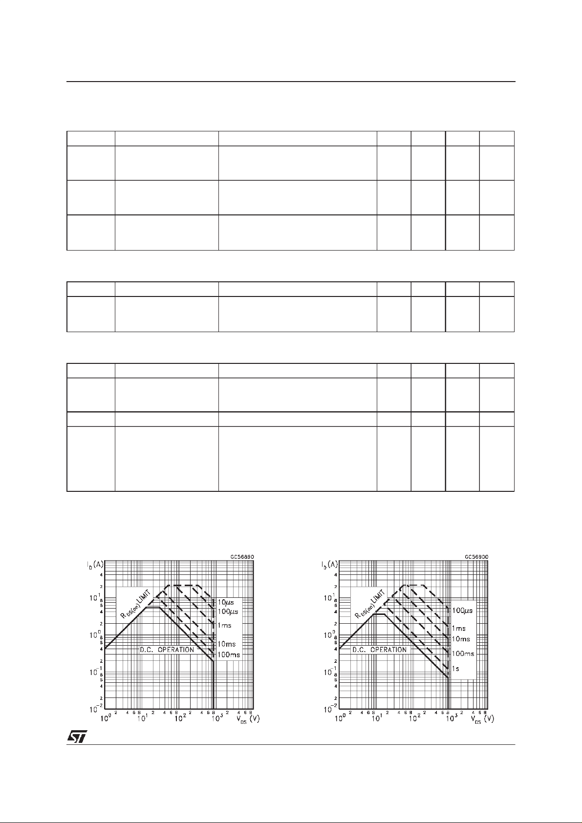
SafeOperating Area for TO-247 SafeOperating Area for ISOWATT218
3/10
Page 4

STW6NA80-STH6NA80FI
ThermalImpedancefor TO-247
DeratingCurve for TO-247
ThermalImpedancefor ISOWATT218
DeratingCurve for ISOWATT218
OutputCharacteristics
4/10
TransferCharacteristics
Page 5

STW6NA80-STH6NA80FI
Transconductance
Gate Charge vs Gate-sourceVoltage
Static Drain-sourceOn Resistance
CapacitanceVariations
Normalized Gate ThresholdVoltage vs
Temperature
Normalized On Resistancevs Temperature
5/10
Page 6

STW6NA80-STH6NA80FI
Turn-onCurrent Slope
Cross-overTime
Turn-offDrain-sourceVoltage Slope
SwitchingSafe Operating Area
AccidentalOverload Area
6/10
Source-drainDiode Forward Characteristics
Page 7

STW6NA80-STH6NA80FI
Fig. 1:
UnclampedInductive LoadTest Circuit
Fig. 3: SwitchingTimes Test CircuitsFor
ResistiveLoad
Fig. 2:
UnclampedInductiveWaveform
Fig. 4: Gate Charge test Circuit
Fig. 5:
Test CircuitFor InductiveLoad Switching
And Diode Recovery Times
7/10
Page 8

STW6NA80-STH6NA80FI
TO-247 MECHANICAL DATA
DIM.
MIN. TYP. MAX. MIN. TYP. MAX.
A 4.7 5.3 0.185 0.209
D 2.2 2.6 0.087 0.102
E 0.4 0.8 0.016 0.031
F 1 1.4 0.039 0.055
F3 2 2.4 0.079 0.094
F4 3 3.4 0.118 0.134
G 10.9 0.429
H 15.3 15.9 0.602 0.626
L 19.7 20.3 0.776 0.779
L3 14.2 14.8 0.559 0.413 0.582
L4 34.6 1.362
L5 5.5 0.217
M 2 3 0.079 0.118
Dia 3.55 3.65 0.140 0.144
mm inch
8/10
P025P
Page 9

ISOWATT218MECHANICAL DATA
STW6NA80-STH6NA80FI
DIM.
mm inch
MIN. TYP. MAX. MIN. TYP. MAX.
A 5.35 5.65 0.210 0.222
C 3.3 3.8 0.130 0.149
D 2.9 3.1 0.114 0.122
D1 1.88 2.08 0.074 0.081
E 0.75 1 0.029 0.039
F 1.05 1.25 0.041 0.049
G 10.8 11.2 0.425 0.441
H 15.8 16.2 0.622 0.637
L1 20.8 21.2 0.818 0.834
L2 19.1 19.9 0.752 0.783
L3 22.8 23.6 0.897 0.929
L4 40.5 42.5 1.594 1.673
L5 4.85 5.25 0.190 0.206
L6 20.25 20.75 0.797 0.817
M 3.5 3.7 0.137 0.145
N 2.1 2.3 0.082 0.090
U 4.6 0.181
L3
N
E
A
D
C
L5
M
H
L2
L6
L1
D1
F
U
G
123
L4
P025C
9/10
Page 10

STW6NA80-STH6NA80FI
Information furnished is believed to be accurate and reliable. However, STMicroelectronics assumes no responsibility forthe consequences
of use of such information nor for any infringement of patents or other rights of third parties which may result from its use. No license is
granted by implication or otherwise under any patent or patent rights of STMicroelectronics. Specification mentioned in this publication are
subject to change withoutnotice. This publication supersedes and replaces all informationpreviously supplied. STMicroelectronics products
are not authorized for use as critical components in life support devices orsystems without express written approval of STMicroelectronics.
The ST logois a registeredtrademark of STMicroelectronics
1998 STMicroelectronics – Printedin Italy – All Rights Reserved
STMicroelectronics GROUP OF COMPANIES
Australia - Brazil - Canada -China -France -Germany - Italy - Japan -Korea -Malaysia - Malta -Mexico - Morocco -The Netherlands -
Singapore - Spain - Sweden -Switzerland - Taiwan- Thailand - UnitedKingdom -U.S.A.
http://www.st.com
.
10/10
 Loading...