

Page 1
STW5NB90
N - CHANNEL 900V - 2.3Ω - 5.6A - TO-247
PowerMESH MOSFET
TYPE V
DSS
R
DS(on)
I
D
ST W 5N B 90 90 0 V < 2.5 Ω 5.6 A
■ TYPICALR
■ EXTREMELYHIGH dv/dtCAPABILITY
■ 100%AVALANCHETESTED
■ VERYLOW INTRINSIC CAPACITANCES
■ GATECHARGE MINIMIZED
DS(on)
= 2.3 Ω
DESCRIPTION
Using the latesthigh voltage MESH OVERLAY
process, STMicroelectronics has designed an
advanced family of power MOSFETs with
outstanding performances. The new patent
pending strip layout coupled with the Company’s
proprietary edge termination structure, gives the
lowest R
per area, exceptional avalanche
DS(on)
and dv/dt capabilities and unrivalled gate charge
and switching characteristics.
APPLICATIONS
■ SWITCHMODE POWER SUPPLIES(SMPS)
■ DC-AC CONVERTERS FOR WELDING
EQUIPMENTAND UNINTERRUPTIBLE
POWERSUPPLIESAND MOTORDRIVE
■ HIGHCURRENT, HIGH SPEED SWITCHING
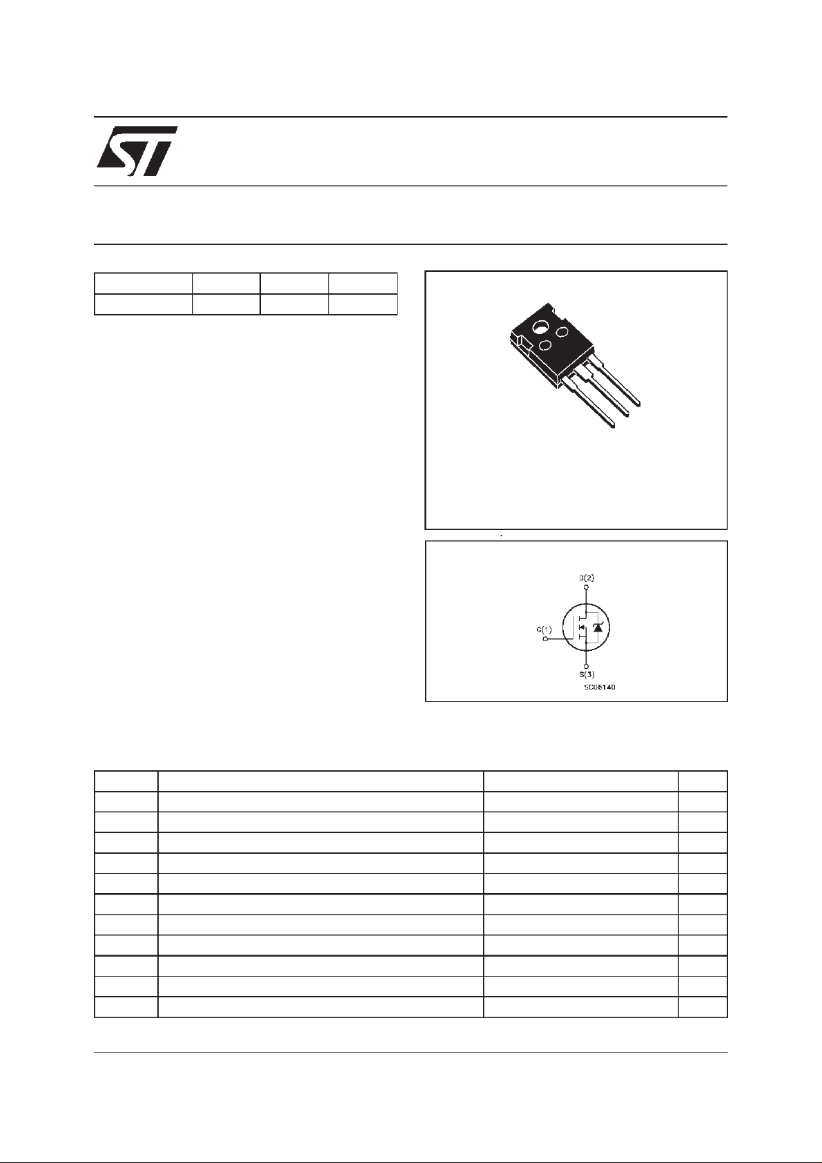
3
2
1
TO-247
INTERNAL SCHEMATIC DIAGRAM
ABSOLUTE MAXIMUM RATINGS
Symbol Parameter Value Unit
V
V
V
I
DM
P
dv/dt(
T
(•) Pulsewidth limited by safe operating area (1)ISD≤ 5A, di/dt ≤ 200A/µs, VDD≤ V
March 1999
Drain-source Voltage (VGS=0) 900 V
DS
Dra in- gate Voltage (RGS=20kΩ)
DGR
Gate -sourc e Vo ltage ± 30 V
GS
I
Drain Current (co ntinuous) at Tc=25oC5.6A
D
I
Drain Current (co ntinuous) at Tc=100oC3.3A
D
900 V
(•) Drain Current (pulsed) 22.4 A
Total Dissipation a t Tc=25oC160W
tot
Derating Factor 1.28 W/
1) Peak Diode Rec ov e ry volt age slop e 4 V/ns
St orage T emper ature -65 t o 1 50
stg
T
Max. Op er a t ing J unction Tem pe r at u re 150
j
,Tj≤T
(BR)DSS
JMAX
o
C
o
C
o
C
1/8
Page 2
STW5NB90
THERMAL DATA
R
thj-case
Rthj-a mb
R
thc-sink
T
AVALANCHE CHARACTERISTICS
Symbol Para meter Max Val ue Uni t
I
AR
E
Ther mal Resis t an ce Junc ti on-cas e Max
Ther mal Resis t an ce Junc ti on-ambien t Max
Thermal Resistance Case-sink Typ
Maximum Lead Temperat u r e Fo r Soldering Purp os e
l
Avalanche Cu rrent, Repetitive or No t -Repet it ive
(pulse width limited by T
Single Pulse Avalanche Energ y
AS
(starting T
=25oC, ID=IAR,VDD=50V)
j
max)
j
0.78
30
0.1
300
5.6 A
284 mJ
o
C/W
oC/W
o
C/W
o
C
ELECTRICAL CHARACTERISTICS (T
=25oC unless otherwisespecified)
case
OFF
Symbol Parameter Test Conditions Min. Typ. M ax. Unit
V
(BR)DSS
Drain-sourc e
=250µAVGS=0
I
D
900 V
Break d own V o lt age
I
DSS
I
GSS
Zero Gate Voltage
Drain Current (V
GS
Gat e- b ody Le akage
Current (V
DS
=0)
=0)
V
=MaxRating
DS
= Max Rating Tc=125oC
V
DS
= ± 30 V
V
GS
1
50
± 100 nA
ON(∗)
Symbol Parameter Test Conditions Min. Typ. M ax. Unit
V
GS(th)
Gate Threshold
V
DS=VGSID
= 250 µA
345V
Voltage
R
DS(on)
Static Drain-source On
VGS=10V ID=2.5 A 2.3 2.5
Resistanc e
I
D(on)
On S t ate Drain Current VDS>I
D(on)xRDS(on)max
5.6 A
VGS=10V
DYNAMIC
Symbol Parameter Test Conditions Min. Typ. M ax. Unit
g
(∗)Forward
fs
Tr ansconduc tance
C
C
C
Input Cap ac i t ance
iss
Out put Capacita nce
oss
Reverse Transf er
rss
Capacitance
VDS>I
D(on)xRDS(on)maxID
=2.5A 2.5 4.1 S
VDS=25V f=1MHz VGS= 0 1250
128
13
µA
µ
Ω
pF
pF
pF
A
2/8
Page 3
STW5NB90
ELECTRICAL CHARACTERISTICS
(continued)
SWITCHINGON
Symbol Parameter Test Conditions Min. Typ. M ax. Unit
t
d(on)
Turn-on Time
t
r
Rise Time
VDD= 450 V ID=2.5A
=4.7 Ω VGS=10V
R
G
18
9
(see test circu it, figure 3)
Q
Q
Q
Total Gate Charge
g
Gat e- Source Cha rge
gs
Gate-Drain Charge
gd
VDD= 720 V ID=5 A VGS=10V
=4.7 Ω VGS=10V
R
G
33
10
13
47 nC
SWITCHINGOFF
Symbol Parameter Test Conditions Min. Typ. M ax. Unit
t
r(Voff)
t
t
Off -voltage Rise Ti me
Fall Time
f
Cross-ov er Time
c
VDD= 720 V ID=5A
=4.7 Ω VGS=10V
R
G
(see test circu it, figure 5)
13
10
17
SOURCEDRAINDIODE
Symbol Parameter Test Conditions Min. Typ. M ax. Unit
I
SD
I
SDM
V
SD
t
Q
I
RRM
(∗) Pulsed: Pulse duration = 300 µs, dutycycle 1.5%
(•) Pulse width limited by safeoperating area
Source-drain Curr ent
(•)
Source-drain Curr ent
5.6
22.4
(pulsed)
(∗) F or ward On Volt age ISD=5A VGS=0 1.6 V
Reverse Reco very
rr
Time
Reverse Reco very
rr
= 5 A di/d t = 100 A/µs
I
SD
= 100 V Tj=150oC
V
DD
(see test circu it, figure 5)
700
5.4
Charge
Reverse Reco very
15.5
Current
ns
ns
nC
nC
ns
ns
ns
A
A
ns
µ
A
C
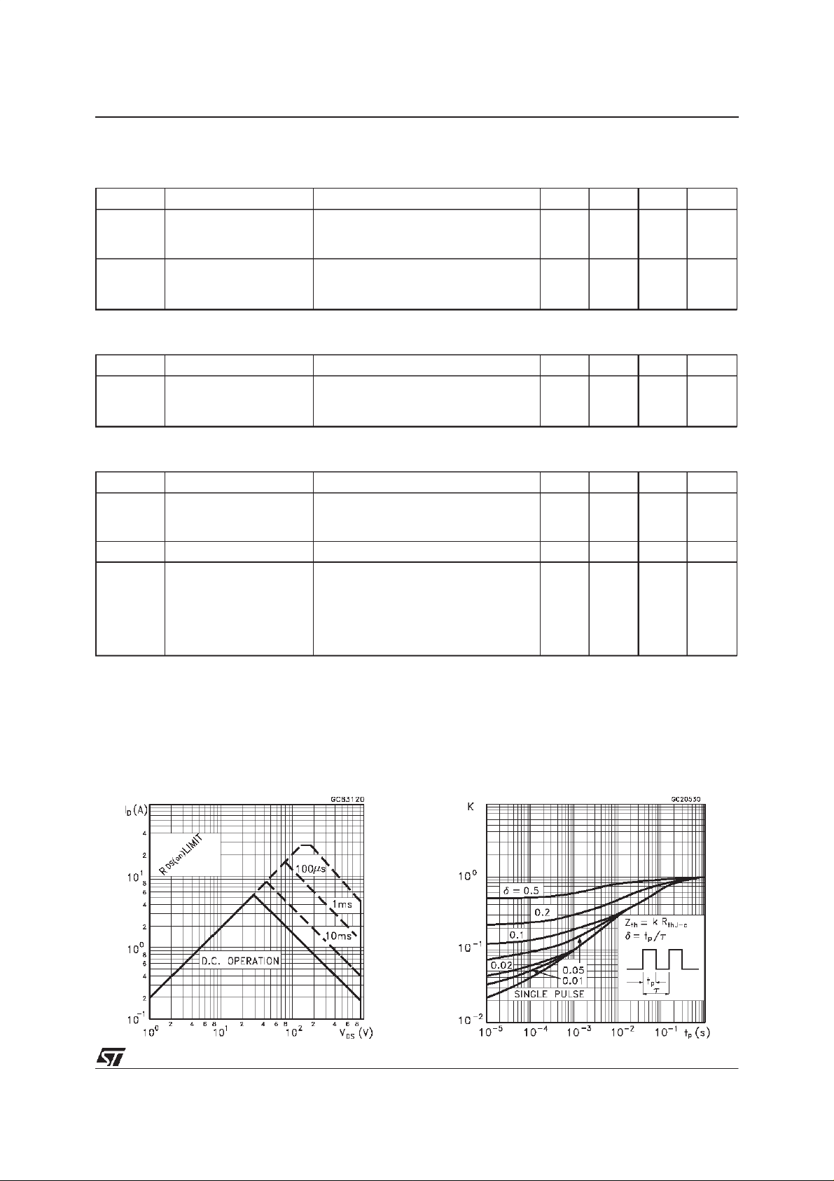
SafeOperating Area Thermal Impedance
3/8
Page 4

STW5NB90
OutputCharacteristics
Transconductance
TransferCharacteristics
Static Drain-sourceOn Resistance
Gate Charge vs Gate-sourceVoltage
4/8
CapacitanceVariations
Page 5

STW5NB90
Normalized Gate ThresholdVoltage vs
Temperature
Source-drainDiode Forward Characteristics
Normalized On Resistancevs Temperature
5/8
Page 6

STW5NB90
Fig. 1:
UnclampedInductive Load Test Circuit
Fig. 3: SwitchingTimes Test CircuitsFor
ResistiveLoad
Fig. 2:
UnclampedInductive Waveform
Fig. 4: Gate Charge test Circuit
Fig. 5:
Test CircuitFor InductiveLoad Switching
And Diode Recovery Times
6/8
Page 7

TO-247 MECHANICAL DATA
STW5NB90
DIM.
MIN. TYP. MAX. MIN. TYP. MAX.
A 4.7 5.3 0.185 0.209
D 2.2 2.6 0.087 0.102
E 0.4 0.8 0.016 0.031
F 1 1.4 0.039 0.055
F3 2 2.4 0.079 0.094
F4 3 3.4 0.118 0.134
G 10.9 0.429
H 15.3 15.9 0.602 0.626
L 19.7 20.3 0.776 0.779
L3 14.2 14.8 0.559 0.413 0.582
L4 34.6 1.362
L5 5.5 0.217
M 2 3 0.079 0.118
Dia 3.55 3.65 0.140 0.144
mm inch
P025P
7/8
Page 8

STW5NB90
Information furnished is believed tobeaccurateand reliable.However, STMicroelectronics assumes no responsibilityforthe consequences
of use of such information nor for any infringement of patents or other rights of third parties which may resultfrom its use. No license is
granted by implication or otherwise under any patent or patent rights of STMicroelectronics. Specificationmentioned in thispublication are
subjecttochange without notice. This publicationsupersedesandreplaces all information previouslysupplied. STMicroelectronicsproducts
are not authorized for use as critical components in lifesupport devices or systemswithout express written approval of STMicroelectronics.
The STlogo is a trademark ofSTMicroelectronics
1999 STMicroelectronics – Printed in Italy – All Rights Reserved
STMicroelectronics GROUP OF COMPANIES
Australia - Brazil -Canada - China - France - Germany - Italy - Japan - Korea - Malaysia - Malta - Mexico - Morocco - The Netherlands -
8/8
Singapore - Spain - Sweden - Switzerland - Taiwan - Thailand - United Kingdom - U.S.A.
http://www.st.com
.
 Loading...