

Page 1
TYPE V
STW5NA90
STH5NA90FI
DSS
900 V
900 V
STW5NA90
STH5NA90FI
N - CHANNEL ENHANCEMENT MODE
POWER MOS TRANSISTORS
PRELIMINARY DATA
R
DS(on)
<2.5Ω
<2.5Ω
I
D
5.3 A
3.5 A
■ TYPICALR
■ ±
30 V GATE-TO-SOURCEVOLTAGE
DS(on)
=2.1 Ω
RATING
■ 100% AVALANCHETESTED
■ REPETITIVEAVALANCHEDATAAT 100
■ GATECHARGEMINIMISED
■ REDUCEDTHRESHOLD VOLTAGESPREAD
o
C
APPLICATIONS
■ HIGH CURRENT, HIGH SPEEDSWITCHING
■ SWITCHMODEPOWER SUPPLY (SMPS)
■ DC-ACCONVERTERS FOR WELDING
EQUIPMENTAND UNINTERRUPTIBLE
POWERSUPPLIES AND MOTORDRIVE
ABSOLUTE MAXIMUM RATINGS
3
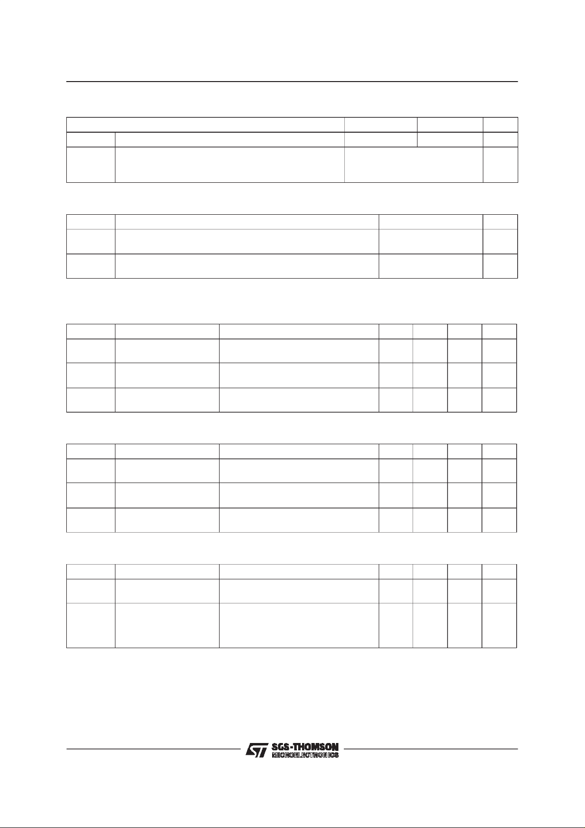
2
1
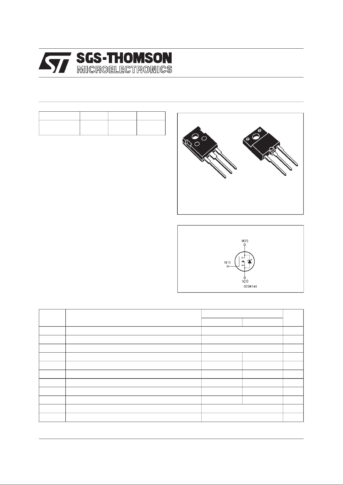
1
TO-247 ISOWATT218
INTERNAL SCHEMATIC DIAGRAM
3
2
Symbol Parameter Valu e Unit
ST W5NA90 ST H5N A90 FI
V
V
DGR
V
I
DM
P
Drain-source V oltage (VGS= 0 ) 900 V
DS
Drain- gate Voltage (RGS=20kΩ)
Gate-s ource Volt age ± 30 V
GS
I
Drain Current (continuous) at Tc=25oC5.33.5A
D
I
Drain Current (continuous) at Tc=100oC3.42.2A
D
900 V
(•) Drain Current (pulsed ) 21.2 21.2 A
Total Dissipation at Tc=25oC 150 60 W
tot
Derat ing Fa c t or 1.2 0.48 W/
V
T
(•) Pulsewidth limited by safe operatingarea
Ins ulation W ithstand Volt a ge (D C) 4000 V
ISO
Storage T emperat ure -65 to 150
stg
T
Max. Operating Junct i on Tem pe r ature 150
j
January 1998
o
C
o
C
o
C
1/6
Page 2
STW5NA90-STH5NA90FI
THERMAL DATA
TO - 2 47 IS O WATT 218
R
thj-case
R
thj-amb
R
thc-sin k
T
AVALANCHE CHARACTERISTICS
Symbol Para met e r Max Va lue Uni t
I
AR
E
Ther mal Resist ance Junction-c a s e Max 0.83 2.08
Ther mal Resist ance Junction-ambient M ax
Ther mal Resist ance Case-sink Ty p
Maximum Lead T e mperature Fo r Soldering Pur p ose
l
Avalanche C ur rent, Rep et it i v e or Not-Repetitive
(pulse width limited by T
Single Pulse Avalanche Energy
AS
(starting T
=25oC, ID=IAR,VDD=50V)
j
max, δ <1%)
j
30
0.1
300
5.3 A
520 mJ
o
C/W
o
C/W
o
C/W
o
C
ELECTRICAL CHARACTERISTICS (T
=25oC unlessotherwise specified)
case
OFF
Symbol Parameter Test C ondition s Min. Typ. Max. Unit
V
(BR)DSS
Drain-source
=250µAVGS=0
I
D
900 V
Breakdown Voltage
I
I
DSS
GSS
Zer o Gate Vo ltage
Drain Cur rent (V
GS
Gat e-body Leak a ge
Current (V
DS
=0)
=0)
=MaxRating
V
DS
V
=MaxRating Tc=100oC
DS
= ± 30 V
V
GS
25
250
±100 nA
ON (∗)
Symbol Parameter Test C ondition s Min. Typ. Max. Unit
V
GS(th )
Gate Threshold
V
DS=VGSID
=250µA
2.25 3 3.75 V
Voltage
R
DS(on)
I
D(on)
Stati c D rain-source On
Resistance
VGS=10V ID=2.5A
=10V ID=2.5A Tc=100oC
V
GS
On St at e D rain Cu r re nt VDS>I
D(on)xRDS(on)max
5.3 A
2.1 2.5
5
VGS=10V
DYNAMIC
Symbol Parameter Test C ondition s Min. Typ. Max. Unit
g
(∗)Forward
fs
Tr ansconductance
C
C
C
Input Capaci t an ce
iss
Out put Capacitance
oss
Reverse T rans fer
rss
Capa cit an c e
VDS>I
D(on)xRDS(on)maxID
=2.5A 4 6.4 S
VDS=25V f=1MHz VGS= 0 1350
150
40
1900
210
60
µA
µA
Ω
Ω
pF
pF
pF
2/6
Page 3

STW5NA90-STH5NA90FI
ELECTRICAL CHARACTERISTICS (continued)
SWITCHINGON
Symbol Parameter Test C ondition s Min. Typ. Max. Unit
t
d(on)
t
r
(di/dt)
Turn-on T ime
Rise T ime
Turn-on Cur rent Slope VDD=720V ID=5A
on
VDD=450V ID=
2.5 A
=4.7 Ω VGS=10V
R
G
=47 Ω VGS=10V
R
G
13
12
250 A/ µ s
20
19
ns
ns
Q
Q
Q
Total Gate Charge
g
Gat e-Source Charge
gs
Gate-Drain Charge
gd
VDD=720V ID=5A VGS=10V 60
10
26
80 nC
SWITCHINGOFF
Symbol Parameter Test C ondition s Min. Typ. Max. Unit
t
r(Voff)
t
t
Of f - voltage Ris e Tim e
Fall Time
f
Cross-over Tim e
c
VDD=720V ID=5A
=4.7 Ω VGS=10V
R
G
15
7
25
25
14
40
SOURCE DRAIN DIODE
Symbol Parameter Test C ondition s Min. Typ. Max. Unit
I
SD
I
SDM
V
SD
t
Q
I
RRM
(∗) Pulsed: Pulse duration =300 µs,duty cycle 1.5 %
(•) Pulse width limited by safe operating area
Source-drain Current
(•)
Source-drain Current
5.3
21.3
(pulsed)
(∗) For ward On Voltage ISD=5.3A VGS=0 1.6 V
Reverse Recovery
rr
Time
Reverse Recovery
rr
= 5 A di/dt = 100 A/µs
I
SD
V
=30V Tj=150oC
DD
1150
17.3
Charge
Reverse Recovery
30
Current
nC
nC
ns
ns
ns
A
A
ns
µC
A
3/6
Page 4

STW5NA90-STH5NA90FI
TO-247 MECHANICAL DATA
DIM.
MIN. TYP. MAX. MIN. TYP. MAX.
A 4.7 5.3 0.185 0.209
D 2.2 2.6 0.087 0.102
E 0.4 0.8 0.016 0.031
F 1 1.4 0.039 0.055
F3 2 2.4 0.079 0.094
F4 3 3.4 0.118 0.134
G 10.9 0.429
H 15.3 15.9 0.602 0.626
L 19.7 20.3 0.776 0.779
L3 14.2 14.8 0.559 0.413 0.582
L4 34.6 1.362
L5 5.5 0.217
M 2 3 0.079 0.118
Dia 3.55 3.65 0.140 0.144
mm inch
4/6
P025P
Page 5

ISOWATT218MECHANICAL DATA
STW5NA90-STH5NA90FI
DIM.
mm inch
MIN. TYP. MAX. MIN. TYP. MAX.
A 5.35 5.65 0.210 0.222
C 3.3 3.8 0.130 0.149
D 2.9 3.1 0.114 0.122
D1 1.88 2.08 0.074 0.081
E 0.75 1 0.029 0.039
F 1.05 1.25 0.041 0.049
G 10.8 11.2 0.425 0.441
H 15.8 16.2 0.622 0.637
L1 20.8 21.2 0.818 0.834
L2 19.1 19.9 0.752 0.783
L3 22.8 23.6 0.897 0.929
L4 40.5 42.5 1.594 1.673
L5 4.85 5.25 0.190 0.206
L6 20.25 20.75 0.797 0.817
M 3.5 3.7 0.137 0.145
N 2.1 2.3 0.082 0.090
U 4.6 0.181
L3
N
E
A
D
C
L5
M
H
L2
L6
L1
D1
F
U
G
123
L4
P025C
5/6
Page 6

STW5NA90-STH5NA90FI
Information furnished is believed to be accurate and reliable. However, SGS-THOMSON Microelectronics assumes no responsability for the
consequences of use of such information nor for any infringement of patents or other rights of third parties which may results from its use. No
license is granted by implication or otherwise under any patent orpatent rights of SGS-THOMSON Microelectronics. Specifications mentioned
in thispublication are subject to change without notice. This publication supersedes and replaces all information previously supplied.
SGS-THOMSON Microelectronics products are not authorized for useas criticalcomponentsin life support devices or systems without express
written approval ofSGS-THOMSON Microelectonics.
1998 SGS-THOMSON Microelectronics - Printed in Italy - All Rights Reserved
Australia - Brazil - Canada - China - France - Germany - Italy - Japan- Korea - Malaysia - Malta - Morocco - The Netherlands -
Singapore - Spain - Sweden - Switzerland - Taiwan - Thailand - United Kingdom - U.S.A
6/6
SGS-THOMSON Microelectronics GROUP OF COMPANIES
...
 Loading...