

Page 1
TYPE V
STW5NA100
STH5NA100FI
DSS
1000 V
1000 V
STW5NA100
STH5NA100FI
N - CHANNEL ENHANCEMENT MODE
POWER MOS TRANSISTORS
PRELIMINARY DATA
R
DS(on)
< 3.5 Ω
< 3.5 Ω
I
D
4.6 A
2.9 A
■ TYPICAL R
■ ± 30V GATE TO SOURCE VOLTAGE RATING
■ 100% AVALANCHE TESTED
■ REPETITIVE AVA LANCHE DATA AT 100
■ GATE CHARGE MINIMISED
■ REDUCED THRESHOLD VO LTA GE SPREA D
DS(on)
= 2.9 Ω
o
C
APPLICATIONS
■ HIGH CURRENT, HIGH SPE ED SWI TCHING
■ SWITCH MODE POWER SUPPLY (SMPS)
■ DC-AC CONVE RTERS FOR WELDING
EQUIPMENT AND UNINTERRUPTIBLE
POWER SUPPLIES AND MOTOR DRIVE
ABSOLUTE MAXIMUM RATINGS
3
2
1
1
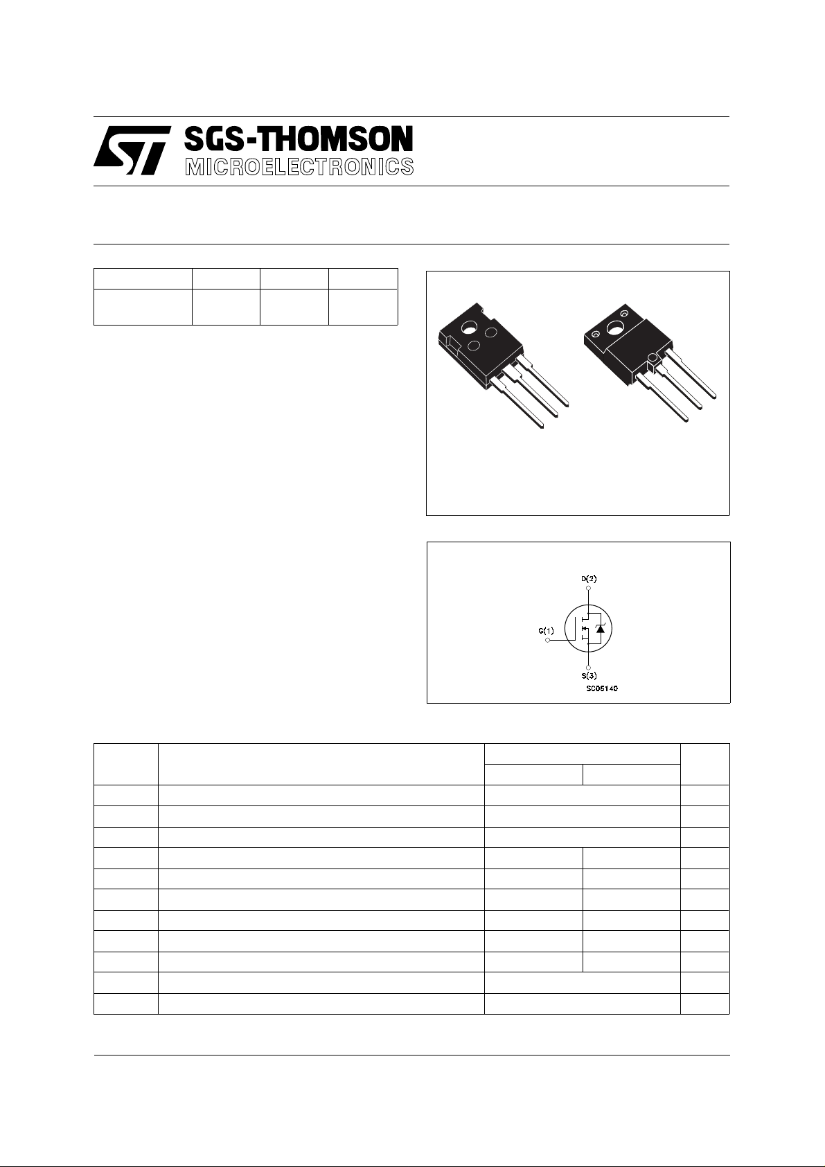
TO-247 ISOWATT2 18
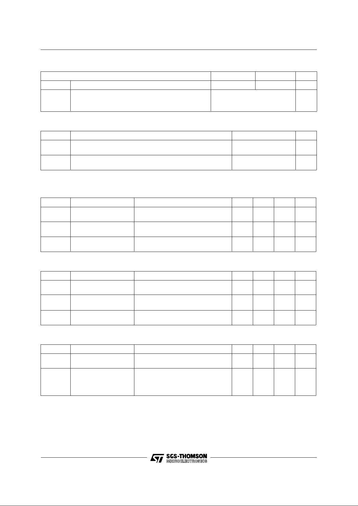
INTER NAL SCH E M ATI C DIAG RA M
3
2
Symbol Parameter Value Unit
STW5NA100 STH5NA100FI
V
V
V
DS
DGR
GS
I
D
I
D
Drain-source Voltage (VGS = 0) 1000 V
Drain- gate Voltage (RGS = 20 kΩ)
1000 V
Gate-source Voltage ± 30 V
Drain Current (continuous) at Tc = 25 oC 4.6 2.9 A
Drain Current (continuous) at Tc = 100 oC 2.9 1.8 A
IDM(•) Drain Cu rrent (pulsed) 18.4 18.4 A
P
Total Dissipation at Tc = 25 oC 150 60 W
tot
Derating Factor 1.2 0.48 W/oC
V
T
(•) Pulse width limited by safe operating area
Insulation Withstand Voltage (DC) 4000 V
ISO
Storage Temperature -65 to 150
stg
T
Max. Operating Junction Temperature 150
j
October 1997
o
C
o
C
1/6
Page 2
STW5NA100-ST H5NA100FI
THERMAL DATA
TO-247 ISOWATT218
R
thj-case
R
thj-amb
R
thc-sink
T
AVALANCHE CHARACTERI S TICS
Symbol Parameter Max Value Unit
I
AR
E
Thermal Resistance Junction-case Max 0.83 2.1
Thermal Resistance Junction-ambient Max
Thermal Resistance Case-sink Typ
Maximum Lead Temperature For Soldering Purpose
l
Avalanche Current, Repetitive or Not-Repetitive
(pulse width limited by T
Single Pulse Avalanche Energy
AS
(starting T
= 25 oC, ID = IAR, V
j
ma x, δ < 1%)
j
= 50 V)
DD
30
0.1
300
4.2 A
160 mJ
o
C/W
o
C/W
o
C/W
o
C
ELECTRICAL CHARACTERISTICS (T
= 25 oC unless otherwise specified)
case
OFF
Symbol Parameter Test Conditions Min. Typ. Max. Unit
V
(BR)DSS
Drain-source
I
= 250 µA V
D
GS
= 0
1000 V
Breakdown Voltage
I
DSS
I
GSS
Zero Gate Voltage
Drain Current (V
GS
Gate-body Leakage
Current (V
DS
= 0)
= 0)
= Max Rating
V
DS
V
= Max Rating Tc = 100 oC
DS
V
= ± 30 V
GS
50
250
±100 nA
ON (∗)
Symbol Parameter Test Conditions Min. Typ. Max. Unit
V
GS(th)
Gate Threshold
V
= VGS ID = 250 µA
DS
2.25 3 3.75 V
Voltage
R
DS(on)
Static Drain-source On
VGS = 10V ID = 2.1 A 2.9 3.5 Ω
Resistance
I
D(on)
On State Drain Current VDS > I
V
= 10 V
GS
D(on)
x R
DS(on)max
4.2 A
DYNAMIC
Symbol Parameter Test Conditions Min. Typ. Max. Unit
g
(∗) Forward
fs
Transconductance
C
C
C
Input Capacitance
iss
Output Capacitance
oss
Reverse Transfer
rss
Capacitance
VDS > I
V
DS
x R
D(on)
DS(on)max
= 25 V f = 1 MHz V
ID = 2.1 A 2 5.5 S
31
2150
165
41
= 0 1650
GS
127
µA
µA
Ω
pF
pF
pF
2/6
Page 3

STW5NA100-ST H5NA10 0FI
ELECTRICAL CHARACTERISTICS (continued)
SWITCHING O N
Symbol Parameter Test Conditions Min. Typ. Max. Unit
t
d(on)
Q
Q
Q
SWITCHING O F F
Symbol Parameter Test Conditions Min. Typ. Max. Unit
t
r(Voff)
t
SOURCE DRAIN DIO DE
Symbol Parameter Test Conditions Min. Typ. Max. Unit
I
SD
I
SDM
V
SD
t
Q
I
RRM
(∗) Pulsed: Pulse duration = 300 µs, duty cycle 1.5 %
(•) Pulse width limited by safe operating area
Turn-on Time
Rise Time
t
r
Total Gate Charge
g
Gate-Source Charge
gs
Gate-Drain Charge
gd
Off-voltage Rise Time
Fall Time
t
f
Cross-over Time
c
Source-drain Current
(•)
Source-drain Current
V
= 500 V ID =
DD
2.1 A
R
= 4.7 Ω VGS = 10 V
G
V
= 800 V ID = 4.2 A V
DD
V
= 800 V ID = 4.2A
DD
= 4.7 Ω VGS = 10 V
R
G
GS
14
12
= 10 V 59
9.4
26.5
94
30
142
20
16
83 nC
132
42
199
4.6
18.4
(pulsed)
(∗) Forward On Voltage ISD = 4.2 A VGS = 0 1.6 V
Reverse Recovery
rr
Time
Reverse Recovery
rr
I
= 4.2 A di/dt = 100 A/µs
SD
V
= 30 V Tj = 150 oC
DD
1000
14
Charge
Reverse Recovery
28
Current
ns
ns
nC
nC
ns
ns
ns
A
A
ns
µC
A
3/6
Page 4

STW5NA100-STH5NA100FI
TO-247 MECHANICAL DATA
DIM.
MIN. TYP. MAX. MIN. TYP. MAX.
A 4.7 5.3 0.185 0.209
D 2.2 2.6 0.087 0.102
E 0.4 0.8 0.016 0.031
F 1 1.4 0.039 0.055
F3 2 2.4 0.079 0.094
F4 3 3.4 0.118 0.134
G 10.9 0.429
H 15.3 15.9 0.602 0.626
L 19.7 20.3 0.776 0.779
L3 14.2 14.8 0.559 0.413 0.582
L4 34.6 1.362
L5 5.5 0.217
M 2 3 0.079 0.118
Dia 3.55 3.65 0.140 0.144
mm inch
4/6
P025P
Page 5

STW5NA100-STH5NA100FI
ISOWATT218 MECHANICAL DATA
DIM.
MIN. TYP. MAX. MIN. TYP. MAX.
A 5.35 5.65 0.210 0.222
C 3.3 3.8 0.130 0.149
D 2.9 3.1 0.114 0.122
D1 1.88 2.08 0.074 0.081
E 0.75 1 0.029 0.039
F 1.05 1.25 0.041 0.049
G 10.8 11.2 0.425 0.441
H 15.8 16.2 0.622 0.637
L1 20.8 21.2 0.818 0.834
L2 19.1 19.9 0.752 0.783
L3 22.8 23.6 0.897 0.929
L4 40.5 42.5 1.594 1.673
L5 4.85 5.25 0.190 0.206
L6 20.25 20.75 0.797 0.817
M 3.5 3.7 0.137 0.145
N 2.1 2.3 0.082 0.090
U4.6 0.181
mm inch
L3
N
E
A
D
C
L5
L2
L6
D1
F
M
U
H
G
123
L1
L4
P025C
5/6
Page 6

STW5NA100-ST H5NA100FI
Information furnished is believed to be accurate and reliable. However, SGS-THOMSON Microelectronics assumes no responsability for the
consequences of use of such information nor for any infringement of patents or other rights of third parties which may results from its use. No
license is granted by implication or ot h erwise under any patent or patent rights of SGS-THOMSON Microelectronics. Specifi cations mentioned
in this publication are subject to change without notice. This publication sup ersedes and replaces all information previously supplied.
SGS-THOMSON Microelectronics products are not authorized for use as critical components in life support devices or systems without express
written approval of SGS-THOMSON Microelectonics.
© 1997 SGS-THOMSON Microelectronics - Printed in Italy - All Rights Reserved
Australia - Brazil - Canada - China - France - Germany - Hong Kong - Italy - Japan - Korea - Malaysia - Malta - Morocco - The Netherlands -
Singapore - Spain - Sweden - Switzerland - Taiwan - Thailand - United Kingdom - U.S.A
SGS-THOMSON Microelectronics GROUP OF COMPANIES
. . .
6/6
 Loading...