

Page 1
STW50N10
N - CHANNEL ENHANCEMENT MODE
POWER MOS TRANSISTOR
TYPE V
DSS
R
DS(on)
I
D
STW50N10 100 V < 0.035 Ω 50 A
■ TYPICALR
■ AVALANCHERUGGEDTECHNOLOGY
■ 100% AVALANCHETESTED
■ REPETITIVEAVALANCHE DATA AT 100
■ HIGH CURRENTCAPABILITY
o
■ 175
■ APPLICATIONORIENTED
COPERATINGTEMPERATURE
DS(on)
=0.027 Ω
o
C
CHARACTERIZATION
APPLICATIONS
■ HIGH CURRENT, HIGH SPEEDSWITCHING
■ POWERMOTORCONTROL
■ DC-DC& DC-AC CONVERTERS
■ SYNCRONOUSRECTIFICATION
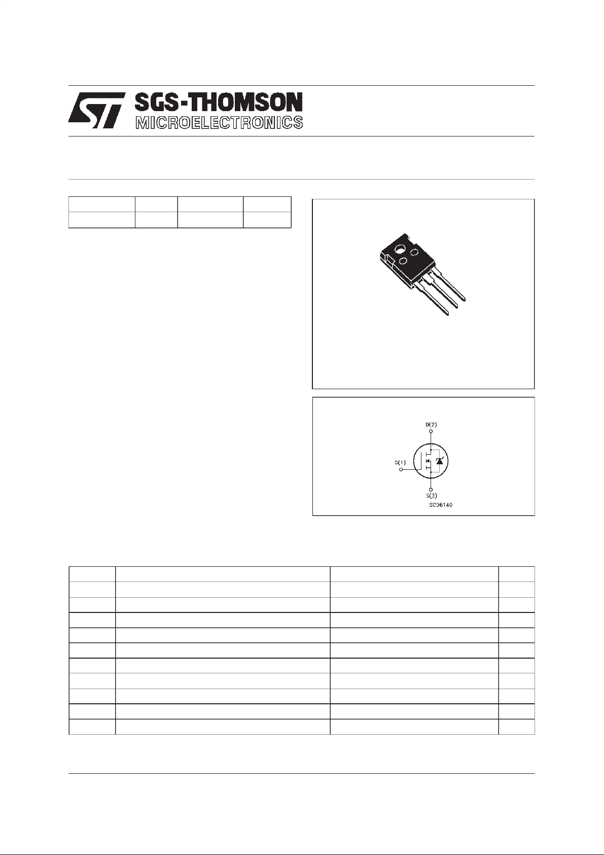
3
2
1
TO-247
INTERNAL SCHEMATIC DIAGRAM
ABSOLUTE MAXIMUM RATINGS
Symbol Parameter Value Unit
V
V
DGR Drain- gate Voltag e (R
V
I
DM
P
T
(•) Pulsewidth limitedby safe operating area ISD≤ 60 A, di/dt ≤ 200 A/µs,VDD≤ V
January 1998
Drain-s ou r ce V olt age ( VGS= 0) 100 V
DS
=20kΩ)
GS
Gate-source Voltage ± 20 V
GS
I
Drain Current (c ontinuous ) at Tc=25oC50A
D
I
Drain Current (c ontinuous ) at Tc=100oC35A
D
100 V
(•) Drain Current (pulsed) 200 A
Tot al Di s sipa t ion at Tc=25oC 180 W
tot
Derating Factor 1.2 W/
Storage Temperature -65 to 175
stg
T
Max. Operating J un c tion T emperature 175
j
(BR)DSS,Tj≤TJMAX
o
C
o
C
o
C
1/8
Page 2
STW50N10
THERMAL DATA
R
thj-case
R
thj-amb
R
thc-sin k
T
AVALANCHE CHARACTERISTICS
Symbol Para met e r Max Value Uni t
I
AR
E
Ther mal Resist ance Junction- case Max
Ther mal Resist ance Junction- ambient Max
Ther mal Resist ance Case-sink Ty p
Maximum Lead Temperat ure For Soldering Purpose
l
Avalanche Current, Repetit ive or Not- Re petitive
(pulse w idth limited by T
Single Pulse Avalanche Energy
AS
(starting T
=25oC, ID=IAR,VDD=25V)
j
max, δ <1%)
j
0.83
30
0.1
300
50 A
400 mJ
o
C/W
o
C/W
o
C/W
o
C
ELECTRICAL CHARACTERISTICS (T
=25oC unlessotherwise specified)
case
OFF
Symbol Parameter Test Condition s Min. Typ. Max. Un it
V
(BR)DSS
Drain-sourc e
=250µAVGS=0
I
D
100 V
Breakdown Voltage
I
I
DSS
GSS
Zer o Gate Vo lt age
Drain Cur re nt (V
GS
Gat e-body Leakage
Current (V
DS
=0)
=0)
=MaxRating
V
DS
V
=MaxRating Tc=125
DS
o
C
= ± 20 V
V
GS
1
10
± 100 nA
ON (∗)
Symbol Parameter Test Condition s Min. Typ. Max. Un it
V
GS(th )
Gate Threshold
V
DS=VGSID
=250µA
234V
Voltage
R
DS(on)
Stati c Drain-so urce On
VGS=10V ID= 25 A 0.027 0.035 Ω
Resistance
I
D(on)
On State Drain Cu rr e nt VDS>I
D(on)xRDS(on)max
50 A
VGS=10V
DYNAMIC
Symbol Parameter Test Condition s Min. Typ. Max. Un it
g
(∗)Forward
fs
Tr ansconductance
C
C
C
Input Capaci t an c e
iss
Out put Capa citanc e
oss
Reverse Transfer
rss
Capa cit an c e
VDS>I
D(on)xRDS(on)maxID
=25A 20 45 S
VDS=25V f=1MHz VGS= 0 4100
600
150
5200
800
200
µA
µA
pF
pF
pF
2/8
Page 3
STW50N10
ELECTRICAL CHARACTERISTICS (continued)
SWITCHINGON
Symbol Parameter Test Condition s Min. Typ. Max. Un it
t
d(on)
Q
Q
Q
Turn-on Time
Rise Tim e
t
r
Total Gate Charge
g
Gat e-Sour ce Charge
gs
Gate-Drain Charge
gd
VDD=50V ID=25A
=4.7 Ω VGS=10V
R
G
VDD=80V ID=50A VGS= 10 V 120
25
75
20
50
SWITCHINGOFF
Symbol Parameter Test Condition s Min. Typ. Max. Un it
t
r(Voff)
t
t
Of f - voltage Rise T im e
Fall Time
f
Cross-ov er Tim e
c
VDD=80V ID=50A
=4.7 Ω VGS=10V
R
G
30
35
65
SOURCE DRAIN DIODE
Symbol Parameter Test Condition s Min. Typ. Max. Un it
I
SD
I
SDM
V
SD
t
Q
I
RRM
(∗) Pulsed: Pulse duration =300 µs, duty cycle 1.5 %
(•) Pulse widthlimited by safeoperating area
1)I
≤ 60 A, di/dt≤ 200 A/µs, VDD≤ V
(
SD
Source-drain Current
(•)
Source-drain Current
(pulsed)
(∗) For ward O n Voltage ISD=50A VGS=0 1.5 V
Reverse Recover y
rr
Time
Reverse Recover y
rr
= 50 A di/dt = 10 0 A/µs
I
SD
=30V Tj=150oC
V
DD
Charge
Reverse Recover y
Current
(BR)DSS,Tj≤TJMAX
35
105
170 nC
45
50
95
50
200
200
1.4
14
ns
ns
nC
nC
ns
ns
ns
A
A
ns
µC
A
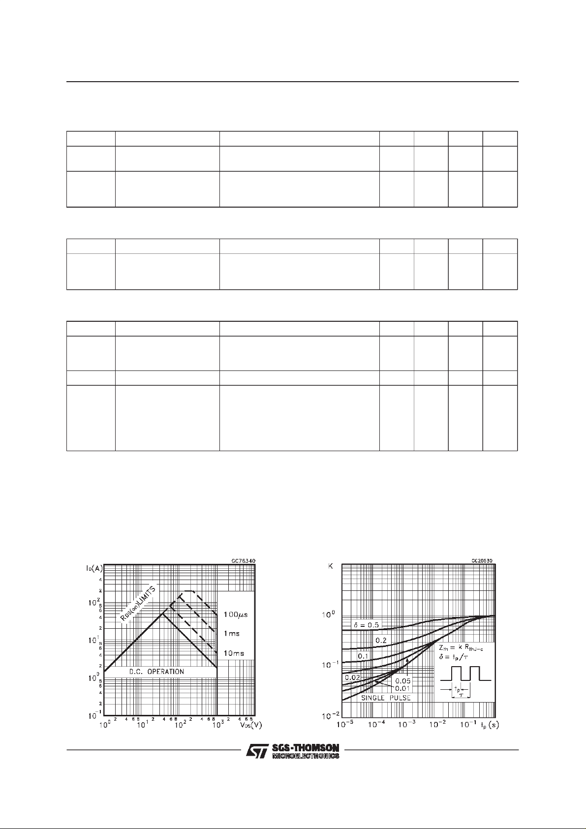
Safe Operating Area ThermalImpedance
3/8
Page 4

STW50N10
OutputCharacteristics
Transconductance
TransferCharacteristics
StaticDrain-sourceOn Resistance
GateCharge vs Gate-sourceVoltage
4/8
CapacitanceVariations
Page 5

STW50N10
Normalized GateThresholdVoltage vs
Temperature
Source-drainDiode Forward Characteristics
Normalized On Resistancevs Temperature
5/8
Page 6

STW50N10
Fig. 1: UnclampedInductiveLoad Test Circuit
Fig. 3: Switching Times Test CircuitsFor
ResistiveLoad
Fig. 2: UnclampedInductive Waveform
Fig. 4: Gate Charge test Circuit
Fig. 5: Test Circuit For Inductive Load Switching
And Diode RecoveryTimes
6/8
Page 7

TO-247 MECHANICAL DATA
STW50N10
DIM.
MIN. TYP. MAX. MIN. TYP. MAX.
A 4.7 5.3 0.185 0.209
D 2.2 2.6 0.087 0.102
E 0.4 0.8 0.016 0.031
F 1 1.4 0.039 0.055
F3 2 2.4 0.079 0.094
F4 3 3.4 0.118 0.134
G 10.9 0.429
H 15.3 15.9 0.602 0.626
L 19.7 20.3 0.776 0.779
L3 14.2 14.8 0.559 0.413 0.582
L4 34.6 1.362
L5 5.5 0.217
M 2 3 0.079 0.118
Dia 3.55 3.65 0.140 0.144
mm inch
P025P
7/8
Page 8

STW50N10
Information furnished is believed tobe accurate and reliable. However, SGS-THOMSON Microelectronics assumes no responsability for the
consequences of use of such information nor for any infringement of patents orother rightsof third parties which may results from itsuse. No
license is granted by implication or otherwiseunder any patent orpatentrights of SGS-THOMSON Microelectronics. Specifications mentioned
in thispublication are subjectto change without notice.This publication supersedes and replaces allinformation previously supplied.
SGS-THOMSON Microelectronics productsare not authorizedfor use as criticalcomponents in life support devicesor systems without express
written approval ofSGS-THOMSON Microelectonics.
1998 SGS-THOMSONMicroelectronics - Printed in Italy - All Rights Reserved
Australia - Brazil - Canada - China - France - Germany - Italy - Japan - Korea- Malaysia- Malta - Morocco - The Netherlands -
Singapore - Spain- Sweden - Switzerland - Taiwan - Thailand - United Kingdom -U.S.A
8/8
SGS-THOMSON MicroelectronicsGROUP OF COMPANIES
...
 Loading...