

Page 1

®
USB CIF/VGA Digital Camera Chipset
STV0672-chipsetf-3-1.fm 29 November 2000
1/41
VV6410/VV6500 &STV0672
Commercial in confidence
The USB camera chipsets from STMicroelectronics are at the
heart of a variety of products which have proven to be highly
successful in a demanding marketplace. Supported by
comprehensive reference designs, technical backup and
fully-featured software drivers, STMicroelectronics offers
camera manufacturers the opportunity to benefit from rapid
time to market with a product of proven quality.
The VV6410/VV6500 are ColorMOS
TM
digital CMOS sensors
that deliver outstanding picture quality. These CIF/VGAresolution sensors have been created specifically tomeet the
standards required for personal video communications. Both
sensors feature automatic black and dark level calibration to
ensure optimum image quality.
The STV0672 co-processor receives image data from the
sensor, that is processed, compressed and passed to the
USB port. It incorporates a digital video processor engine,
which performs automatic exposure, automatic gain control
and automatic white balance, together with colour matrixing,
gamma correction, peaking, automatic defect correction and
noise cancellation logic. This data is then compressed to
deliver high frame rates with minimum impact on image
quality. The USB interface supports USB isochronous data
transfer mode. This data transfer mode allows the user to
specifiy the percentage of USB bandwidth to allocate to a
USB device, thus allowing multiple cameras/other USB
peripherals to be connected to a single USB hub.
The chipset is backed by a fully-featured driver which
provides a host of user-definable settings for optimum
camera setup. The user interface supports a degree of
customisation.
STMicroelectronics offers a range of support services to
guarantee product quality, including test specifications and
test software.
• Real-time video - up to 30fps CIF,15fps VGA
• Multiple output video modes supported
• USB 1.1 compliant
• Motion-JPEG compression
• Isochronous USB data transfer
• Automatic black and dark level calibration
• Full VfW and TWAIN driver support
• Integrated voltage regulation
• Pixel defect detection and correction
• Minimal BOM for complete USB camera
• Programmable vendor ID
• USB Camera
• Biometric identification
• Toys and games
Pixel resolution 352 x 288 (CIF)
640 x 480 (VGA)
Array size 2.73mm x 2.04mm (CIF)
4.89mm x 3.66mm (VGA)
Exposure control Automatic (to +82dB)
Gain control Automatic (to +30dB)
Signal/Noise
ratio
c.56dB
Supply voltage 4.1v-5.25v DC
(internally regulated)
USB
Compatibility
USB Specification V1.1
Meets full power management
requirements with no external
components required
Supply current approx. 150mA (CIF, 30fps)
approx. 190mA (VGA, 15fps)
Operating
temperature
(ambient)
0
o
C - 40oC
(for extended temp. info please contact STMicroelectronics)
Package type VV6410C036: 36CLCC
VV6500C001: 48CLCC
STV0672: 64TQFP
KEY FEATURES
APPLICATIONS
SPECIFICATIONS
Page 2

STV0672-chipsetf-3-1.fm
29 November 2000
Commercial in confidence
2/41
Table of Contents
1. Document Revision History ............................................................................................ 3
2. Introduction ...................................................................................................................... 4
2.1 STV0672 Chipset General Description ..........................................................................................4
2.2 Video Processor (VP).....................................................................................................................4
2.3 Video Compression (VC) Engine ...................................................................................................7
2.4 Control Processor...........................................................................................................................8
2.5 V6410/VV6500 General Description ..............................................................................................8
2.6 Power Management .......................................................................................................................9
2.7 Suspend Mode .............................................................................................................................11
2.8 Still Image Upload and Remote Wake-Up....................................................................................11
3. External Interfaces......................................................................................................... 12
3.1 USB Interface...............................................................................................................................12
3.2 USB Vendor ID (VID) and Product ID (PID).................................................................................12
3.3 General Purpose Input and Output Signals, Microport, DigiPort and External EEPROM............14
4. Detailed specifications .................................................................................................. 15
4.1 STV0672 Absolute Max Ratings ..................................................................................................15
4.2 STV0672 AC/DC Characteristics .................................................................................................16
4.3 VV6410 Optical Characterisation Data.........................................................................................18
4.4 VV6500 Optical Characterisation Data.........................................................................................19
4.5 VV6410 Power Consumption .......................................................................................................20
4.6 VV6500 Power Consumption .......................................................................................................20
4.7 Digital Input Pad Pull-Up and Pull-Down Strengths (VV6410 and VV6500) ................................21
5. Pinout and pin descriptions.......................................................................................... 22
5.1 VV6410 Pin Details ......................................................................................................................22
5.2 VV6500 Pin Details ......................................................................................................................25
5.3 STV0672 Pin Details ....................................................................................................................28
6. Package Details.............................................................................................................. 31
6.1 VV6410 (36pin CLCC)..................................................................................................................31
6.2 VV6500 (48pin CLCC)..................................................................................................................32
6.3 STV0672 (64pin TQFP)................................................................................................................33
7. VV6410/VV6500+STV0672 Reference Design.............................................................. 34
8. Reference Design and Evaluation Kits (RDK’s and EVK’s)........................................ 38
9. Design Issues.................................................................................................................39
10. Ordering Details .............................................................................................................40
Page 3

Customer Datasheet, Rev 3.1, 29 November 2000 STV0672-chipsetf-3-1.fm
Commercial in confidence
3/41
29 November 2000
1. Document Revision History
Revision Date Comments
1.0 28/06/00 First Advance release
1.1 04/07/00 First Preliminary release
2.0 11/07/00 Add extra sensor information and move to new naming convention for datasheets.
2.1 19/07/00 Minor text corrections and additions
DC Parameters updated
3.0 28/07/00 The document presented in full release status. 0672 AC/DC parameters corrected.
3.1 24/10/00 EEPROM serial data and serial clock pin assignments clarified
Table 1 : Document Revision History
Page 4

STV0672-chipsetf-3-1.fm Introduction
29 November 2000
Commercial in confidence
4/41
2. Introduction
2.1 STV0672 Chipset General Description
The STV0672 is a digital video processor requiring no external RAM and minimum of passive support components to provide a
complete USB camera. STV0672 acceptsraw digital video data from aCIF format CMOS sensor (VV6410) orfrom a VGA format
CMOS sensor (VV6500) and is capable of transferring the resulting YCbCr video data to a host PC over USB at rates up to 30
frames per second (CIF) or 15 frames per second (VGA).
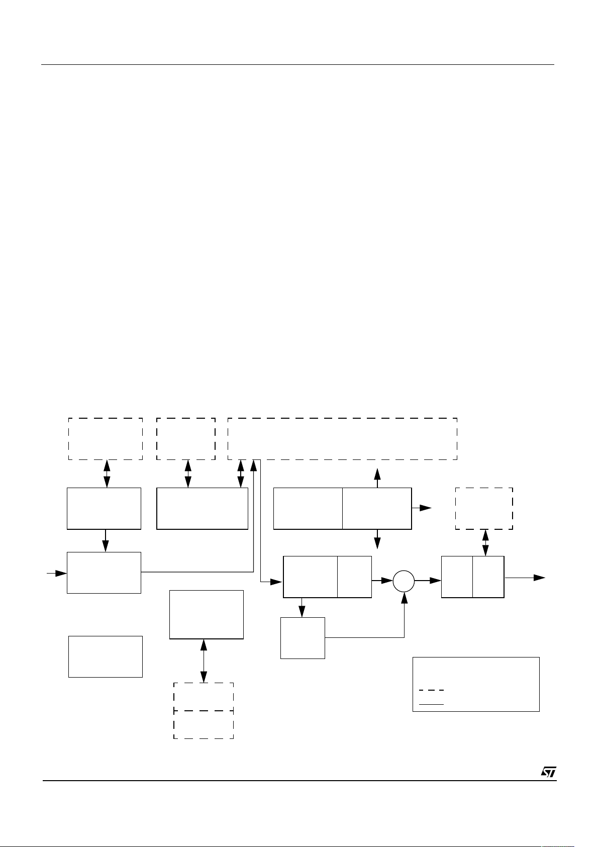
The STV0672 architecture consists of a number of separate functional blocks:
• Video Processor (VP) to include interface logic to sensor
• Video Compressor (VC)
• USB control block
• General purpose control
The VP controls the VVVV6410/VV6500 sensor and processes the raw RGB pixel data into CIF or QCIF YCbCr images
This YCbCr data is compressed by the VC.
The USB control block transfers the compressed data to the host PC. System operation, responding to host requests and
commands as well as performing sensor exposure control and colour balance is handled by the video processor (VP).
2.2 Video Processor (VP)
2.2.1 Video Processor/Sensor Interface
The STV0672 video processor (VP) module provides formatted YCbCr 4:2:2-sampled digital video to the video compressor (VC)
module at frame rates up to 30 frames per second. The VP also interfaces directly to the VV6410/VV6500 image sensors. The
interface to the sensor incorporates:
• A 5-wire data bus SDATA[4:0] for receiving both video data and embedded timing references.
• A 2-wire serial interface SSDA,SSCL to control the sensor (allow reconfiguration of the sensor registers).
• The sensor clock SCLK.
• The sensor regulates the USB system power to 3V3forboth the sensor and the STV0672. The sensor requires one external
simple transistor in conjunction with the internal regulator to provide current drive to be able to successfully power the
complete camera system
• The sensor also provides a power-on-reset signal that is used to reset the STV0672. This power-on-reset signal also resets
the sensor.
• The module supports USB suspend mode.
The simplified block diagram shown below highlights STV0672’s key functional blocks.
Page 5

Customer Datasheet, Rev 3.1, 29 November 2000 STV0672-chipsetf-3-1.fm
Commercial in confidence
5/41
29 November 2000
Figure 1 : Block Diagram of STV0672 Video Processor Module
2.2.1 Video Processor Functions
STV0672 provides a master clock SCLK to the camera module. Each 10-bit pixel value generated by the sensor is transmitted
across the 5wire, (the MSBit of the databus is unused in the current application but it will support future sensors where a 12bit
ADC architecture may be used), databus SDATA[4:0] as a pair of sequential 5-bit nibbles, most significant nibble first. Codes
representing the start and end frames and thestart and end of lines are embedded within the video pixel data stream to allow the
video processor receiver to synchronise with the video data which the sensor is generating.
The video processing engine performs the following functions on incoming data
• full colour restoration at each pixel site from Bayer-patterned input data
• matrixing/gain on each colour channel for colour purity
• peaking for image clarity
• gamma correction
• colour space conversion (including hue and saturation control) from raw RGB to YCbCr[4:2:2].
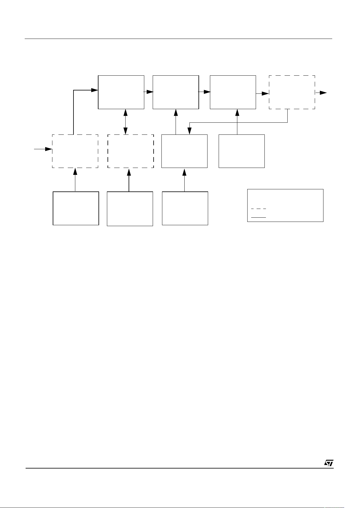
The 2-wire sensor serial interface (SSDA and SSCL) provides control of sensor configuration. Figure 2 below gives a block
overview of the VP module.
2.2.2 Auto Exposure and Gain Control
Control of the sensor exposure is automatically controlled by STV0672. Sensor exposure is evaluated (and, where necessary
Compression EngineMotion JPEG
Video Processor
Stream
DigiPort
D+
D-
Clocks
+ PLL
porb
12MHz
XTAL
8052 Core
ROM
MicroPort I/F
10
15
STV0672
RAM
Serial I/f to EEPROM
(GPIO)
(GPIO)
Compressed Data
Control +
FIFOs
Ext.
Interrupts
USB Port
VV6410
CIF/VGA
Sensor
/VV6500
General purpose
housekeeper functions
including AEC,AGC and
AWB
Video Data[4:0]
SSCL
SSDA
PORB
SCK
SUSPEND
USB Core/Glue
logic and
command FIFO’s
SDA
SCL
RESET
Page 6
STV0672-chipsetf-3-1.fm Introduction
29 November 2000
Commercial in confidence
6/41
modified) once per frame, where a frame consists of 2 video fields. The video fields are identical in length, that is they do not
contain any of the half line detail of the analogue video standards like CCIR or NTSC. Two fields per frame are required by the
internal sensor video timing model. Integration time, sensor analogue gain and STV0672 digital gain are all used to control the
overall exposure. The STV0672 exposure algorithm uses an asymptotic approach in calculating the change required in the
present exposure value to approach the requested exposure target.
2.2.3 Defect Correction
STV0672 automatically detects and corrects for pixel defects, without the need for any additional components or additional
sensor calibration procedures. This greatly simplifies camera assembly and test, when compared with previous EEPROM-based
defect correction schemes. The pixel defect correction scheme in STV0672 ensures that VV6410+STV0672 and
VV6500+STV0672 are ‘defect free’ chipsets.
2.2.4 Interpolation
The Bayer pattern from the sensor providesunder-sampled trichromatic data. Interpolation up-samples these undersampled data
streams to restore a bandlimited (effectively blurred) version of the original, using simple two-dimensional filtering templates.
Signal components aliased in the under-sampling process remain aliased after interpolation. The green channel (no longer
containing notions of even and odd rows) is treated differently from red and blue, being interpolated into two output
representations, one ‘sharper’ (containing more high-frequency detail) than the other. The smoother of the two green signals is
output along with red and blue to the matrix block.
2.2.5 Unsharp masking
Subtraction of these two green representations creates an ‘unsharp mask’, which can be further processed before adding back
into the main colour flow.The unsharp signal undergoes variable coring (a central thresholding operation for noise reduction)and
intensity (gain operation on the cored signal). The strain parameter from the housekeeper acts as both a coring threshold and an
attenuator on the user intensity setting, achieving a softening of image appearance in low-light conditions.
Figure 2 : STV0672 VP Block Diagram
Ram/Data Storage
Logic
Key
===
FPN Vector
FPN Cancel
Input Processor
Set-Up
Registers
Defect Map
Defect
Detect & Correct
Line Store
(9x644x10)
Address Gen
Control
(All Sub Blocks)
Matrix
RAM
ROM
QVGA FIFO
Gamma
YCbCr
Encoder
(644x14)
(128x32)
4:2:2
House Keeper
(AEC,AGC,
AWB etc)
+
IN
OUT
interpolation
Peaking
Page 7

Customer Datasheet, Rev 3.1, 29 November 2000 STV0672-chipsetf-3-1.fm
Commercial in confidence
7/41
29 November 2000
2.2.6 Matrixing
This module performs a 3 x 3 matrix multiplication on the smooth RGB channels, to map pixel taking chromaticities onto nominal
display chromaticities. Depending on the characteristics, ageneral 3 x 3 matrix can effect the transformation;however we choose
to decompose this matrix into the form M = UT, where U is a neutral-preserving matrix, each of whose rows add to unity, and T is
a diagonal matrix of tilts, which form one component of the channel gains applied in the input processor. The combination of U
and T are coded in such a way as to require the user provision of 9 integers; three for the tilts T and six for the off-diagonal
components of U (on-diagonal coefficients are implicit in a re-ordered row computation). The strain parameter from the
housekeeper and a specially-cored version of the unsharp mask signal control the damper; a variable which desaturates the
effect of the matrix by attenuating off-diagonal components in the presence of noise (strain component, occurring in low ambient
light) or Bayer aliasing (unsharp component, occurring in image regions with high edge-content).
2.2.7 Peaking
The unsharp mask signal is added to each matrixed colour channel to compensate for edge information lost in Bayer-pattern
under-sampling and interpolation.
2.2.8 Gamma correction
Gamma correction provides a non-linear distortion of data amplitudes required for various video communication standards, as
well as cosmetic enhancement of image detail.
2.2.9 Coder
The coder module comprises a color-space convertor which takes RGB from the gamma module and produces luminance Y and
weighted colour-differences Cb & Cr. The data is now passed in YCbCr form to the Video Compression block.
2.3 Video Compression (VC) Engine
The video compression engine performs 3 main functions:
• Up scaling of input YCbCr 4:2:2 video stream from the VP (typically to scale from QVGA to CIF image formats)
• Compression and Encoding of YCbCr stream into Motion-JPEG (M-JPEG) format
• USB Bandwidth monitoring
Figure 3 below gives a block overview of the VC module. The data stream from the VP can be upto VGA size. The scaler in VC
can downsize this image. Once scaled the video stream is then converted into M-JPEG format. M-JPEG simply treats video as a
series of JPEG still images. Please note that the JPEG specific header information need not be transmitted in a MJPEG stream.
The conversion is realised viaa sequential DCT (Discrete Cosine Transform)with Huffman encoding. After transfer over USB the
M-JPEG stream will be decoded in the Video-for-Windows (VfW) device driver running on the host.
The VC module is capable of compression ratios of up to 100:1 although clearly this is scene dependent. Image framerate
produced by the STV0672 chipset is fixed and furthermore the available USB bandwidth is also fixed (within the software driver).
The VC module varies the compression ratio to match the fluctuating input video data rates, that vary according to scene
dynamics, to the available USB bandwidth and required framerate.
The final stage of the VC block manages the data transfer rate from the local VC FIFO store to the USB core. STV0672 can
perform this management automatically, by employing long-term (frame-level) and short-term (block-level) compression
management. The former is achieved by varying ascalar quality-factor from frame to frame, to drive expecteddata rates upwards
or downwards. The latter is achieved by truncating the zig-zag sequence of AC coefficients more or less severely according to
how many preset thresholds of FIFO usage have been crossed. As FIFO usage approaches maximum, this truncation process
reduces instantaneous data rates until stability is regained, at the cost of local loss of detail in the image. The latter process is
transparent to the decoder. Statistics of threshold-crossing activity are subsequently used in the long-term quality setting
decision.
Page 8
STV0672-chipsetf-3-1.fm Introduction
29 November 2000
Commercial in confidence
8/41
2.4 Control Processor
The embedded 8052 microprocessor core plays a very important role within the STV0672 controlling data flow through the major
sub blocks within STV0672 as well as the I2C communications to reconfigure VP in line with requests from the device driver.
2.5 V6410/VV6500 General Description
The VV6410 sensor is a CIF format, 352 x288 pixels, CMOS image sensor capable of outputting digital pixel data at frame rates,
of up to 30 frames per second. The VV6500 sensor is aVGA format, 640 x 480 pixels,CMOS image sensor capable of outputting
digital pixel data at frame rates, of up to 15 frames per second (in VGA mode). Both sensor arrays are covered by colour filters.
VV6410/VV6500 have on-chip 10-bit analogue to digital converters and are designed to interface directly to the STV0672 coprocessor chip as described above.
DCT
Quantiser
Entropy Coder USB FIFO
8-line RAM
Block RAM
Auto Squeeze Huffman tables
Raster to
block control
row/col/zig-zag
control
Quantisation
tables
Figure 3 : STV0672 VC Block Diagram
Ram/Data Storage
Logic
Key
===
IN
OUT
(stores YUV)
Page 9
Customer Datasheet, Rev 3.1, 29 November 2000 STV0672-chipsetf-3-1.fm
Commercial in confidence
9/41
29 November 2000
2.5.1 Image Format
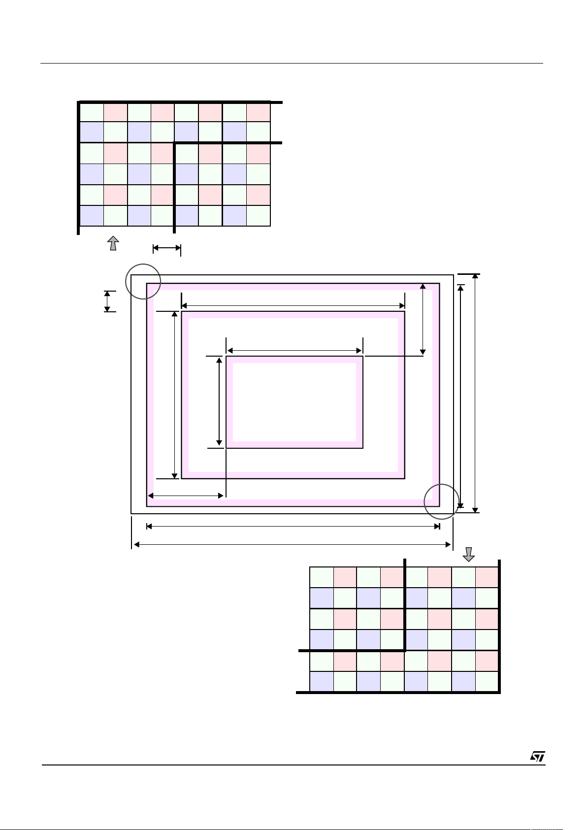
The output image format is either CIF (352 x 288 pixel array) or VGA (640 x 480 pixel array). To provide the colour co-processor
with the extra information it needs for interpolation at the edges of the VV6410/VV6500 pixel array, an additional border 2 pixels
deep on all 4 sides of the array is enabled under serial interface control. The resulting image size of 356 x 292 pixels (or 644 x
484 pixels for VGA) is the default power up state for this sensor. The pixel array is covered by a set of Bayer pattern colour dyes,
see Figure 5 for details.
.
2.6 Power Management
All the power management for the chipset is controlled by the sensor. A series of on board voltage regulators regulate the
incoming VBUS supply to derive all the necessary power supplies required by the camera chipset.
The chipset conforms to all power requirements specified by USB Version 1.1.
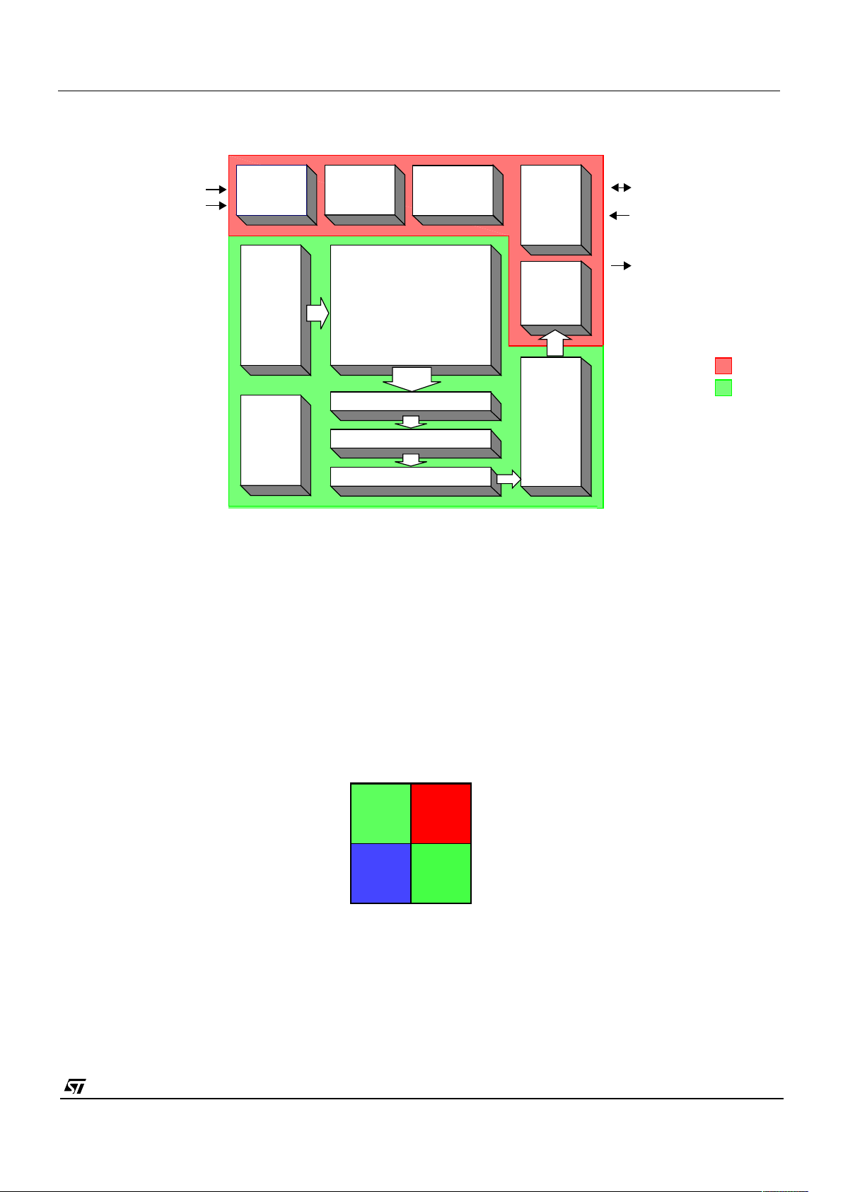
Figure 4 : Block Diagram of VV6410/VV6500 Image Sensor (5-wire output)
OUTPUT
FORMAT
D[4:0]
SSDA
SSCL
SCK
IMAGE
FORMAT
EXPOSURE
CONTROL
SERIAL
INTERFACE
OFFSET
CANCELLATION
Digital Logic
Y-
DECODER
VREGS,
AUDIO AMP.,
& REFS
PHOTO DIODE
ARRAY
Column ADC
Readout
Analogue Core
Structure
X-Decoder
SRAM line store
SUSPEND
Figure 5 : Bayer Colourisation Pattern
Green 1
Blue Green 2
Red
Odd Rows
(5, 7, 9,...)
Even Rows
(4, 6, 8,...)
Odd
Columns
(1,3,5,...)
Even
Columns
(2, 4, 6,...)
Page 10
STV0672-chipsetf-3-1.fm Introduction
29 November 2000
Commercial in confidence
10/41
Blue Green
Green Red
Blue Green
Green Red
644 Pixels
356 Pixels
292 Pixels
484 Pixels
Figure 6 : Image Formats
4321
6
8
7
5
65
1, 2, 3, 4, 5, 6,... ..., 649, 650, 651, 652
5, 6, 7, 8, 9, 10,...
..., 485, 486, 487, 488
144 Pixels
96 Pixels
Blue Green
Green Red
10
9
87
648647646645
484
486
485
483
650649
488
487
652651
488 Pixels
652 Pixels
Blue Green
Green Red
Blue Green
Green Red
Blue Green
Green Red
Blue Green
Green Red
Blue Green
Green Red
Blue Green
Green Red
Blue Green
Green Red
Blue Green
Green Red
Blue Green
Green Red
Blue Green
Green Red
Blue Green
Green Red
Blue Green
Green Red
Blue Green
Green Red
Blue Green
Green Red
Blue Green
Green Red
Blue Green
Green Red
Blue Green
Green Red
Blue Green
Green Red
Blue Green
Green Red
Blue Green
Green Red
Blue Green
Green Red
324 Pixels
244 Pixels
160Pixels
120 Pixels
Page 11

Customer Datasheet, Rev 3.1, 29 November 2000 STV0672-chipsetf-3-1.fm
Commercial in confidence
11/41
29 November 2000
2.7 Suspend Mode
Under the control of the SUSPEND pin VV6410/VV6500 can be forced into an ultra low power mode. The sensor will consume
less than 80µA of current while suspended and the STV0672 device will consume approximately 50µA. The total chipset
consumption therefore is approximately 150µA.
The sensor will enter suspend mode when the SUSPEND pin has been driven high. The SUSPEND mode is effectively identical
to a power-on-reset - all the video timing blocks within the sensor are reset as are the contents of the serial interface, therefore
the user will have to perform a compete reconfiguration of the device on exitting SUSPEND.
2.8 Still Image Upload and Remote Wake-Up
The present STV0672 reference design includes 2 micro switches, identified as SW1 and SW2. Two special functions are
supported by these switches - image upload via a TWAIN driver and remote wake up of the host.
Presently both of these features will be invoked by depressing SW1. If the camera/host is in standby mode then pressing SW1
will force the system to wake up. Thereafter SW1 will control the uploading of still images to the host. It is important to note that
STV0672 must always be used in tethered mode, attached to a PC, and there is no local memory for image storage.
Mode Description Approx. Module Current
Suspend Camera module in lowest power state. Suspend has
been asserted by host. Theclocktosensor has been
removed and all blocks within STV0672 have been
powered down.
c.100µA
Table 2 : STV0672 chipset power consumption
Page 12

STV0672-chipsetf-3-1.fm External Interfaces
29 November 2000
Commercial in confidence
12/41
3. External Interfaces
3.1 USB Interface
The USB Interface is designed to be compliant with the Version 1.1 of the USB Specification. The STV0672 chipset solution is a
High Power Device and is therefore suitable for connection to any USB port on a PC or on a self-powered hub. It will not function
when connected to a bus-powered hub as there may be insufficient power available.
The device fits into the Device Framework specified in Chapter 9 of the USB Specification as follows:
• The device supports a single high power configuration (Configuration 1).
• Endpoint 0 is the default control endpoint and is always supported
• Endpoint 0 supports all of the USB commands required by the device framework.
• Vendor Specific commands on Endpoint 0 are used for all device control.
• Configuration 1 supports a single interface (Interface 0)
• Interface 0 supports 8 alternate settings (Alternates 0-7)
• The alternate settings support between 0 and 2 additional endpoints.
• Endpoint 1 is used for Isochronous transfer of image data
• Endpoint 3 is used for transferring status information, e.g. state of a hardware button.
• The endpoints are configured as follows in the alternate settings:
The best and most consistent performance in terms of image quality will always be obtained in the highest bandwidth setting
(Alternate 7). Under some circumstances it may not be possible for the host to allocate this amount of USB bandwidth to the
device.
The isochronous settings reserve varying quantities of bandwidth - from 10% to 85% of USB bandwidth. The lower settings will
give poor image quality due to heavy compression applied to maintain high framerate streaming of image data, but at the same
time will leave more bandwidth free for other USB devices. This may be more desirable if more than one camera is to be used, or
if there are other isochronous peripherals connected. The device driver allows the user to specify the maximum bandwidth they
wish to allocate to data transfer from the device. If the maximum specified by the user is not available, perhaps because another
isochronous device has already reserved that bandwidth, then lower alternates will be tried until one succeeds.
Benchmark testing of the STV0672 indicates that 30fps CIF video (compressed) can be accomodated in 50% of USB bandwidth.
3.2 USB Vendor ID (VID) and Product ID (PID)
All USB devices will report a VID and PID as part of a Standard Device Descriptor. The VID and PID for STV0672 are configured
Alternate Setting Endpoint1 (Isochronous) Endpoint3 (Interrupt)
0 Not present Not present
1 Not present 8 bytes/packet; 1 packet/8 Frames
2 128 bytes/packet; 1 Packet/frame 8 bytes/packet; 1 packet/8 Frames
3 384 bytes/packet; 1 Packet/frame 8 bytes/packet; 1 packet/8 Frames
4 640 bytes/packet; 1 Packet/frame 8 bytes/packet; 1 packet/8 Frames
5 768 bytes/packet; 1 Packet/frame 8 bytes/packet; 1 packet/8 Frames
6 896 bytes/packet; 1 Packet/frame 8 bytes/packet; 1 packet/8 Frames
7 1023 bytes/packet; 1 Packet/frame 8 bytes/packet; 1 packet/8 Frames
Table 3 : Endpoint Alternate Settings
Page 13
Customer Datasheet, Rev 3.1, 29 November 2000 STV0672-chipsetf-3-1.fm
Commercial in confidence
13/41
29 November 2000
by the state of the Digiport bus bits. The Digiport also controls the device current consumption that is reported to the host at
device enumeration. The current reference designfor the STV0672-chipset has Digiport[7:0] connected toVSS, thus the VID and
PID are 16’h0553 and 16’h0100 respectively.
Digiport bit slice Function
[3:0] Configures the ls nibble of the PID
[5:4] Master VID/PID select
[7:6] Power setting
Table 4 : Basic Digiport Configuration
Digiport[3:0] PID ls nibble
4’b0000 4’b0000
4’b0001 4’b0001
4’b0010 4’b0010
4’b0011 4’b0011
4’b0100 4’b0100
4’b0101 4’b0101
4’b0110 4’b0110
4’b0111 4’b0111
4’b1000 4’b1000
4’b1001 4’b1001
4’b1010 4’b1010
4’b1011 4’b1011
4’b1100 4’b1100
4’b1101 4’b1101
4’b1110 4’b1110
4’b1111 4’b1111
Table 5 : Digiport ls nibble Configuration
Digiport[5:4] VID/PID Reported
2’b00 16’h0553/16’h010x
1
2’b01 16’h0553/16’h011x
2
2’b10 16’h0553/16’h012x
3
Table 6 : Master VID/PID Selection
Page 14
STV0672-chipsetf-3-1.fm External Interfaces
29 November 2000
Commercial in confidence
14/41
3.3 General Purpose Input and Output Signals, Microport, DigiPort and External EEPROM
The present datasheet makes no attempt to discuss some of the peripheral functions that could be offered with the STV0672
chipset. It may be appropriate for such features to be included in a later version of this datasheet.
If any customers require more information on these features please contact STMicroelectronics.
2’b11 16’h0553/16’h013x
4
1. The ‘x’ ls nibble of the PID is defined by the value from Table 5 above
2. The ‘x’ ls nibble of the PID is defined by the value from Table 5 above
3. The ‘x’ ls nibble of the PID is defined by the value from Table 5 above
4. The ‘x’ ls nibble of the PID is defined by the value from Table 5 above
Digiport[7:6] Current consumption reported
2’b00 250mA
2’b01 300mA
2’b10 400mA
2’b11 500mA
Table 7 : Device Power Consumption Indicator
Digiport[5:4] VID/PID Reported
Table 6 : Master VID/PID Selection
Page 15

Customer Datasheet, Rev 3.1, 29 November 2000 STV0672-chipsetf-3-1.fm
Commercial in confidence
15/41
29 November 2000
4. Detailed specifications
4.1 STV0672 Absolute Max Ratings
Description Range Unit
Operating Temperature 0 to 70
o
C
Storage Temperature -50 to 150
o
C
Voltage on USB D+/D- 0 - VDD V
Page 16
STV0672-chipsetf-3-1.fm Detailed specifications
29 November 2000
Commercial in confidence
16/41
4.2 STV0672 AC/DC Characteristics
Parameter Description Min Typ Max Units Comments
VDD Primary STV0672 Power Supply 3.0 3.3 3.6 V
VDDU Power Supply for on-chip USB transceiver 3.0 3.3 3.6 V
I
suspend
STV0672 suspend mode current 20 µA VDD at 3V3
I
active
STV0672 active, high power mode current 150 mA VDD at 3V6 when
streaming VGA video
at 15fps.
I
active
STV0672 active, low power mode current 22 mA VDD at 3V6 with
VV6410 sensor
32 mA VDD at 3V6 with
VV6500 sensor
I
leakage
Leakage current +/-2 µA
V
ILU
USB differential pad D+/D- input low 0.8 V
V
IHU
USB differential pad D+/D- input high (driven)
1
1. These parameters are not measured but STMicroelectronics will guarantee the published values.
2.0 V
V
IHUZ
USB differential pad D+/D- input high (floating)
2
2. These parameters are not measured but STMicroelectronics will guarantee the published values.
2.7 3.6 V
V
DI
USB differential pad D+/D- input sensitivity
3
3. VDI = [(D+) - (D-)
0.2 V
V
CM
USB differential pad D+/D- common mode volt-
age
4
4. VCM includes VDI range.
0.8 2.5 V
V
OLU
USB differential pad D+/D- output low voltage
5
5. These parameters are not measured but STMicroelectronics will guarantee the published values.
0.0 0.3 V
V
OHU
USB differential pad D+/D- output high voltage
6
6. These parameters are not measured but STMicroelectronics will guarantee the published values.
2.8 3.6 V
V
OHU
USB differential pad D+/D- output high voltage
7
7. These parameters are not measured but STMicroelectronics will guarantee the published values.
2.8 3.6 V
V
CRS
USB differential pad D+/D- output signal cross
over voltage
8
8. These parameters are not measured but STMicroelectronics will guarantee the published values.
1.3 2.0 V
V
IL
CMOS input low voltage 0.35VDD V
V
IH
CMOS input high voltage 0.65VDD V
V
T
Threshold point 1.65 V
V
OH
Output high voltage 2.4 V
V
OL
Output low voltage 0.4 V
CLK
in
Input clock frequency
9
9. Although the device is tested at an upper limit of 24MHz, the USB specification version 1.1 states that the maximum clock
input frequency is 12MHz
.
12 24 MHz
Page 17
Customer Datasheet, Rev 3.1, 29 November 2000 STV0672-chipsetf-3-1.fm
Commercial in confidence
17/41
29 November 2000
4.3 Chipset VV6410/VV6500+STV0672
4.1 VV6410 AC/DC Specification
Table 9 : VV6410 DC specification
Mode of Operation VV6410+STV0672 VV6500+STV0672
Standby mode Camera module in lowest power state.
Suspend has been asserted by host.
The clock to sensor has been removed
and all blocks within STV0672 have
been powered down.
c.100µΑ c.100µΑ
Start-up mode STV0672 is in low power mode. Fast
clocks enabled allowing STV0672 to
process commands from host PC. Sen-
sor and video processor module are
held in reset
c.22mA c.32mA
Active mode All STV0672 modules and sensor are
enabled with video data being trans-
ferred to host PC.
c.140mA c.190mA
Table 8 : VV6410/VV6500+STV0672 chipset current consumption
Parameter Comment Units
Image Format 356 x 292 pixels (CIF) -
Pixel Size 7.5 x 6.9 µm
Technology 0.5µm 3 level metal CMOS -
Array Format CIF -
Exposure control range 81
(minimum exposure period 3µs and maximum exposure
period is 33ms)
1
1. We assume CIF (30fps) mode, input clock of 16MHz and internal clock divisor of 1.
db
Supply Voltage 3.0-6.0 DC +/-10% V
Operating Temp. range 0 - 40
o
C
V
OL_max
2
2. This will be worst case reading. Device outputs had significant capacitive loading and supply voltage reduced to 2V7
0.512 V
V
OH_min
3
3. This will be worst case reading. Device outputs had significant capacitive loading and supply voltage reduced to 2V7
2.054 V
V
I_maxL
4
4. This will be worst case reading. Device outputs had significant capacitive loading and supply voltage reduced to 2V7
0.683 V
V
IH_min
5
5. This will be worst case reading. Device outputs had significant capacitive loading and supply voltage reduced to 2V7
2.237 V
Serial interface frequency
range
0-100kHz
Page 18
STV0672-chipsetf-3-1.fm Detailed specifications
29 November 2000
Commercial in confidence
18/41
4.2 VV6500 AC/DC Specification
Table 10 : Preliminary Data for VV6500
4.3 VV6410 Optical Characterisation Data
Parameter Comment Units
Image Format 644 x 484pixels (VGA) -
Pixel Size 7.5 x 7.5 µm
Technology 0.5µm 3 level metal CMOS -
Array Format VGA -
Exposure control range 81
(minimum exposure period 3µs and maximum exposure
period is 33ms)
1
1. We assume CIF (30fps) mode, input clock of 16MHz and internal clock divisor of 1.
db
Supply Voltage 3.0-6.0 DC +/-10% V
Operating Temp. range 0 - 40
o
C
V
OL_max
2
2. This is worst case reading. Device outputs had significant capacitive loading and supply voltage reduced to 2V7
TBA V
V
OH_min
3
3. This is worst case reading. Device outputs had significant capacitive loading and supply voltage reduced to 2V7
TBA V
V
I_maxL
4
4. This is worst case reading. Device outputs had significant capacitive loading and supply voltage reduced to 2V7
TBA V
V
IH_min
5
5. This is worst case reading. Device outputs had significant capacitive loading and supply voltage reduced to 2V7
TBA V
Serial interface frequency
range
0-100 kHz
Optical Parameter Min Typical Max Units
Dark Current - 46 - mV/sec
Average Sensitivity - 2.1 - V/lux.sec
Fixed Pattern Noise (FPN) - 1.74 - mV
Vertical Fixed Pattern Noise (VFPN) - 1.2 - mV
Random Noise - 1.17 - mV
Sensor SNR - c.56 - dB
Shading (Gross) - 0.9 - mV
Table 11 : VV6410 Optical Characterisation Data
Page 19
Customer Datasheet, Rev 3.1, 29 November 2000 STV0672-chipsetf-3-1.fm
Commercial in confidence
19/41
29 November 2000
4.4 VV6500 Optical Characterisation Data
4.4.1 Noise Parameters and Dark Current
Various noise parameters are measured on the 410 and 500 series sensors as follows:
• Fixed Pattern Noise (FPN)
• Vertical Fixed Pattern Noise (VFPN)
• Random Noise
• Fine Shading
• Gross Shading
The parameters will be described in more detail below along with the data produced by the characterisation programme.
4.4.2 Blooming
Blooming is a phenomenon that does not affect CMOS sensors in the same way as CCD imagers are afflicted. With a CCD
blooming can cause an entire column/columns to flood and saturate.
CMOS imagers are however affected by a different type of saturation. If an intense light source, (e.g. Maglite torch), is shone at
very close proximity to the image sensor the pixel sampling mechanism will break down and rather than displaying a saturated
white light a black image will occur.
The 410 pixel architecture uses Correlated DoubleSampling (CDS) to help reduce noise in thesystem. The pixel is read normally
first, yielding the true integrated signal information, then the pixel is reset and very quickly read for a second time. This normally
yields black information - as the pixel has had no exposure time - that can be subtracted from the signal from the first read. This
subtraction will remove much of the noise from the pixel leaving only the useful signal information.
In an example where a pixel has saturated in both the first and the second reads due to an intense light source. When the noise
cancellation subtraction operation is then performed the result is close to zero signal from the pixel therefore resulting in the
displayed black image.
We do not perform any test measurements for this phenomenon.
4.4.3 Dark Current
This is defined as the rate at which the average pixel voltage increases overtime with the device not illuminated. The darkcurrent
will be measured at a gain setting of 4 and a clock divisor of 16 at a fixed temperature and will be expressed in mV.
4.4.4 Fixed Pattern Noise
The FPN of an image sensor is the average pixel non-temporal noise divided by the average pixel voltage. The illumination
Optical Parameter Min Typical Max Units
Dark Current - TBA - mV/sec
Average Sensitivity - TBA - V/lux.sec
Fixed Pattern Noise (FPN) - TBA - mV
Vertical Fixed Pattern Noise (VFPN) - TBA - mV
Random Noise - TBA - mV
Sensor SNR - TBA - dB
Shading (Gross) - TBA - mV
Table 12 : VV6500 Optical Characterisation Data
Page 20
STV0672-chipsetf-3-1.fm Detailed specifications
29 November 2000
Commercial in confidence
20/41
source will be white light that has been IR filtered, producing a diffuse uniform illumination at the surface of the sensor package.
The FPN will be calculated at coarse exposure settings of 0,10,150,250 and 302 with gain set to 1. 10 frames are grabbed and
averaged to produce a temporally independent frame before each calculation. FPN will be expressed in mV.
4.4.5 Vertical Fixed Pattern Noise
VFPN describes the spatial noise in an image sensor related to patterns with a vertical orientation. The VFPN is defined as the
standard deviation over all columns of the average pixel voltage for each column determined at zero exposure and zero
illumination. VFPN will be expressed in mV.
4.4.6 Random Noise
Random noise is the temporal noise component within the image. Random noise will be expressed in mV.
4.4.7 Shading
This describes how average pixel values per “block” change across the image sensor array. For fine shading calculations the
image sensor array is split into 30 pixel by 30 pixel blocks. An average value is then calculated for each block and the averages
are then compared across the whole device. The blocks are increased in size to 60 pixels by 60 pixels for the gross shading
calculation. Shading will be expressed in mV.
4.5 VV6410 Power Consumption
4.6 VV6500 Power Consumption
Table 13 : VV6410 Current consumption in different modes
Operating Condition Current Consumption
Low power mode current consumption 5.6mA
Sleep mode current consumption
1
1. Estimated figures - this parameter was not measured during final characterisation
18mA
Suspend mode current consumption
(with CLKIP disabled)
85uA
Normal operating mode current consumption
2
2. Measured while device is clocked at 16MHz and streaming CIF video at 30fps
26.2mA
Operating Condition Current Consumption
Low power mode current consumption 7.6mA
Sleep mode current consumption
1
1. Estimated figures - this parameter was not measured during final characterisation
18mA
Suspend mode current consumption
(with CLKIP disabled)
74uA
Normal operating mode current consumption
2
2. Measured while device is clocked at 24MHz and streaming VGA video at 30fps
42mA (max)
Page 21

Customer Datasheet, Rev 3.1, 29 November 2000 STV0672-chipsetf-3-1.fm
Commercial in confidence
21/41
29 November 2000
4.7 Digital Input Pad Pull-Up and Pull-Down Strengths (VV6410 and VV6500)
Pad Type Pads Min current Max Current
Library pulldown suspend 35µA52µA
Library pullup sclk, sda, oeb 25µA42µA
Custom pullup resetb 66µA 250µA
Table 14 : Pad Pull-up/Pull-down Strengths
Page 22
STV0672-chipsetf-3-1.fm Pinout and pin descriptions
29 November 2000
Commercial in confidence
22/41
5. Pinout and pin descriptions
5.1 VV6410 Pin Details
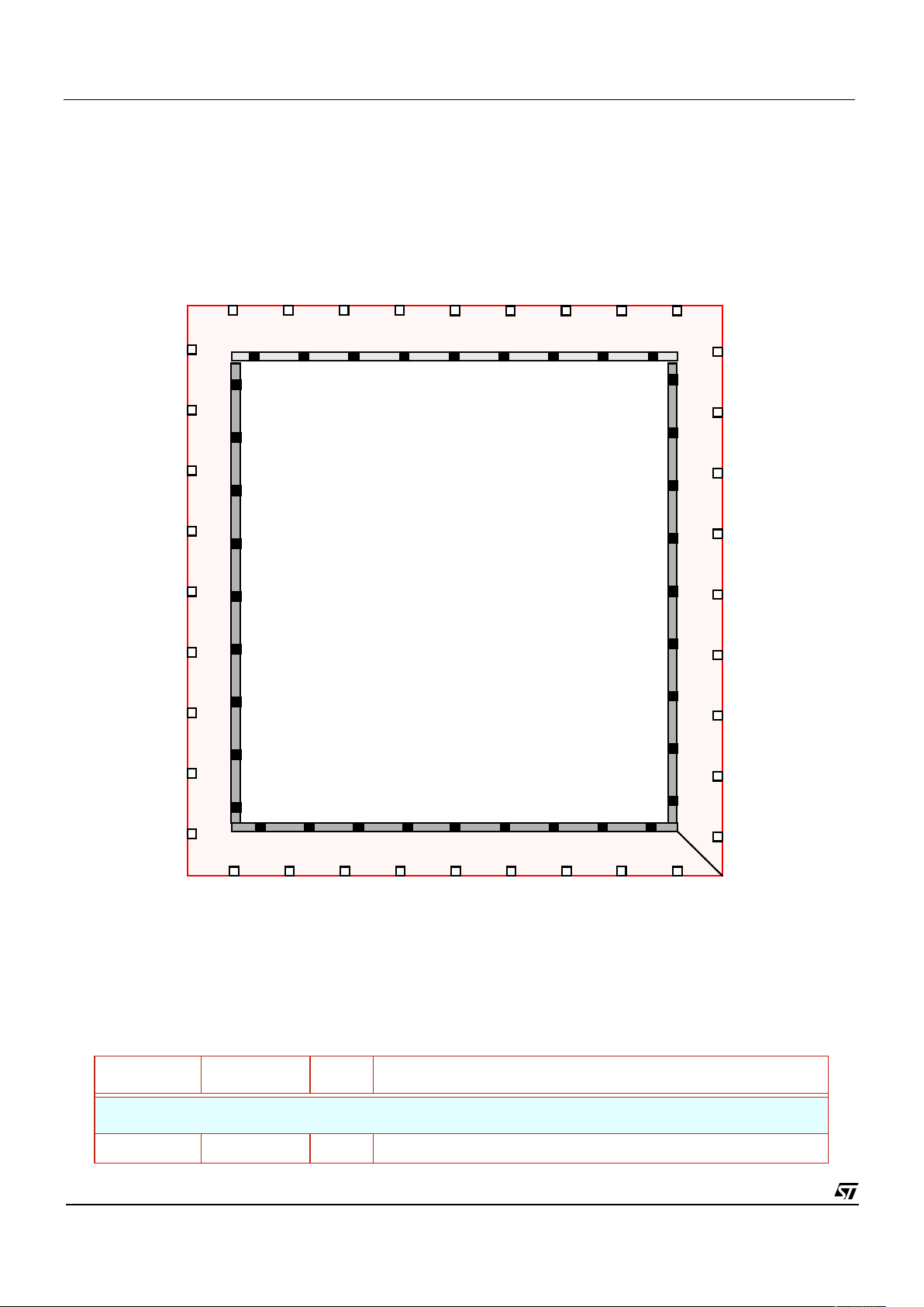
Figure 7 : 36 pin CLCC package pin assignment
Name Pin Number Type Description
POWER SUPPLIES
AVSS 10 GND Core analog ground and reference supplies.
RESETB
D[0]
LST/D[5]
FST/D[6]
VDDcore/
Vbus
VBG
VRT
AoutP
VDDhi
OEB
CLKI
7
8
6
54
3
2
1
9
10
11
12
13
14
15
16
17
19
20
21
22
23
24
25
26
27
28
29
32
33
34 35 36
D[3]
D[4]
Aud3V3
AoutN
Vbase
AVSS
18
30
31
Vbltw
D[1]
Vid3V3
AIN
VSScore
VSSio
SRAMVSS
D[2]
QCK
SDA
SUSPEND
VDDio
D[7]
Vbloom
Reg3V3
SCL
PORB
Page 23
Customer Datasheet, Rev 3.1, 29 November 2000 STV0672-chipsetf-3-1.fm
Commercial in confidence
23/41
29 November 2000
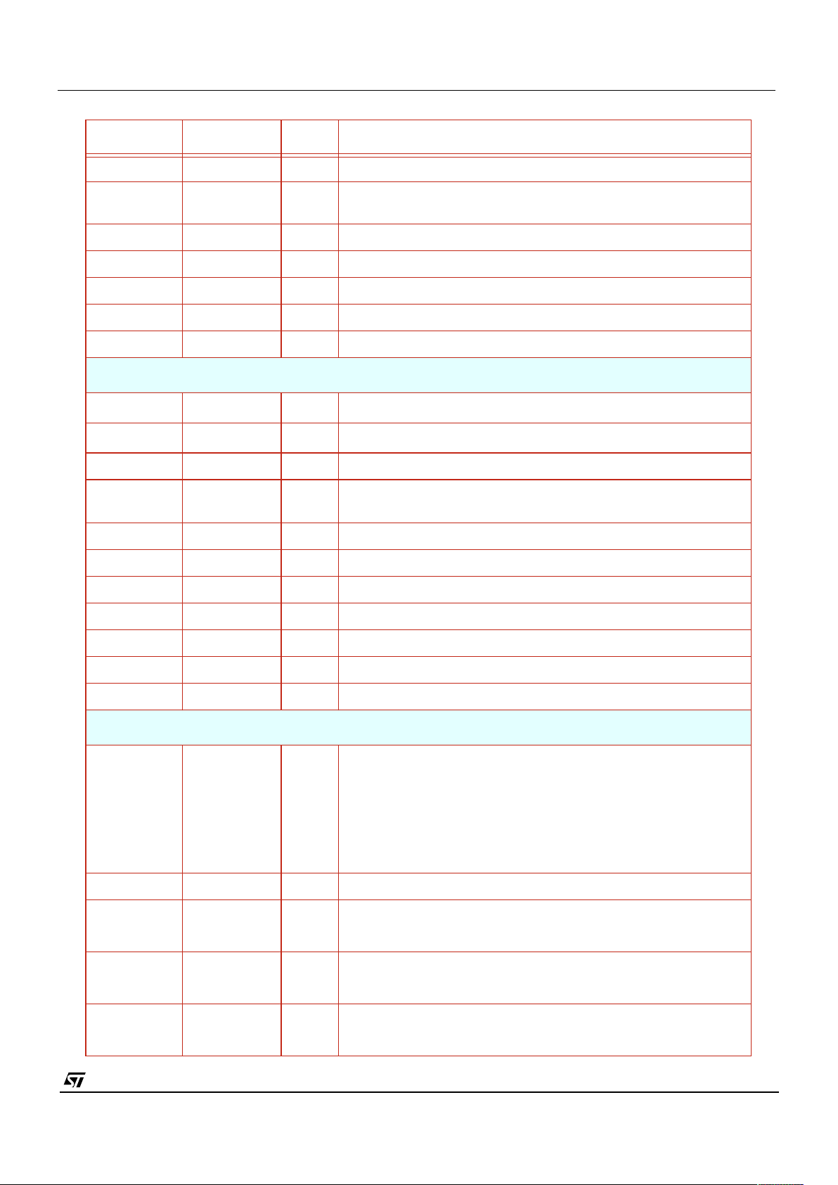
SRAMVSS 17 GND In-column SRAM analog ground.
VDDcore/
Reg3V3
34 PWR Digital logic power.
VDDio 33 PWR Digital pad ring power.
VSScore 22 GND Digital logic ground.
VSSio 23 GND Digital pad ring ground.
Vid3V3 11 PWR On-chip Video Supply Voltage Regulator Output
Aud3V3 3 PWR On-chip Audio Amplifier Voltage Regulator Output
ANALOG SIGNALS
Vbloom
1
8 OA Anti-blooming pixel reset voltage
VBLTW
2
7 OA Bitline test white level reference
VBG 1 OA Internally generated bandgap reference voltage 1.22V
VRT
3
2IAPixel reset voltage (nominally a monitor point but can be overdriven
externally)
VDDHI 9 IA Voltage doubler output, 4.6V -> 4.8V
VBase 35 OA Drive for base of external bipolar
Vbus 36 IA Incoming power supply 3.3 -> 6V
AIN 4 IA Analog input to Audio Amplifier
AOutP 5 OA Analog output of Audio Amplifier (positive)
AOutN 6 OA Analog output of Audio Amplifier (negative)
PORB 13 OD Power-on Reset (Bar) Output.
DIGITAL VIDEO INTERFACE
D[4]
D[3]
D[2]
D[1]
D[0]
27
26
25
24
20
ODT Tri-stateable 5-wire output data bus.
- D[4] is the most significant bit.
- D[4:0] have programmable drive strengths 2, 4 and 6 mA
QCK 32 ODT Tri-stateable data qualification clock.
LST/D[5] 28 ODT Tri-stateable Line start output
May be configured as tri-stateable output data bit 5 D[5].
FST/D[6] 29 ODT Tri-stateable Frame start signal.
May be configured as tri-stateable output data bit 6 D[6].
D[7] 31 ODT Tri-stateable Data wire (ms data bit).
May be configured as tri-stateable output data bit 6 D[6].
Name Pin Number Type Description
Page 24
STV0672-chipsetf-3-1.fm Pinout and pin descriptions
29 November 2000
Commercial in confidence
24/41
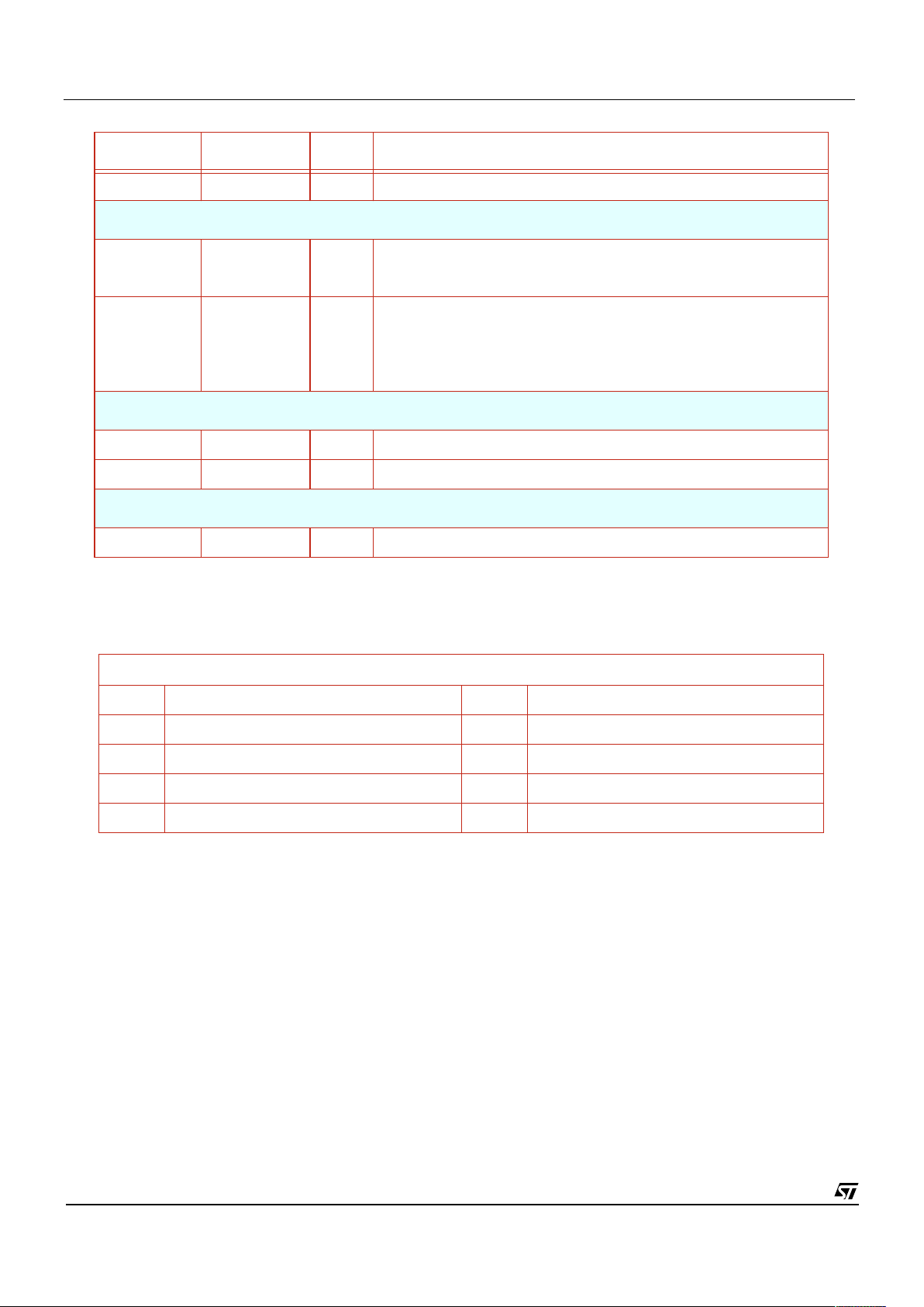
OEB 16 ID↓ Digital output (tri-state) enable.
DIGITAL CONTROL SIGNALS
RESETB 21 ID↑ System Reset. Active Low.
May be configured as System Sync. Active Low.
SUSPEND 12 ID↑ USB Suspend Mode Control signal. Active High
If this feature is not required then the support circuit must pull the pin to
ground. The combination of an active high signal and pull up pad was
chosen to limit current drawn by the device while in suspend mode.
SERIAL INTERFACE
SCL 15 BI↑ Serial bus clock (input only).
SDA 14 BI↑ Serial bus data (bidirectional, open drain).
SYSTEM CLOCKS
CLKI 30 ID↓ Schmitt Buffered Clock input or LVDS positive Clock input
1. Vbloom pin was bonded on pre-production samples but will not be bonded on production parts
2. VBLTW pin was bonded on pre-production samples but will not be bonded on production parts
3. VRT pin was bonded on pre-production samples but will not be bonded on production parts
Key
A Analog Input D Digital Input
OA Analog Output ID↑ Digital input with internal pull-up
BI Bidirectional ID↓ Digital input with internal pull-down
BI↑ Bidirectional with internal pull-up OD Digital Output
BI↓ Bidirectional with internal pull-down ODT Tri-stateable Digital Output
Name Pin Number Type Description
Page 25
Customer Datasheet, Rev 3.1, 29 November 2000 STV0672-chipsetf-3-1.fm
Commercial in confidence
25/41
29 November 2000
5.2 VV6500 Pin Details
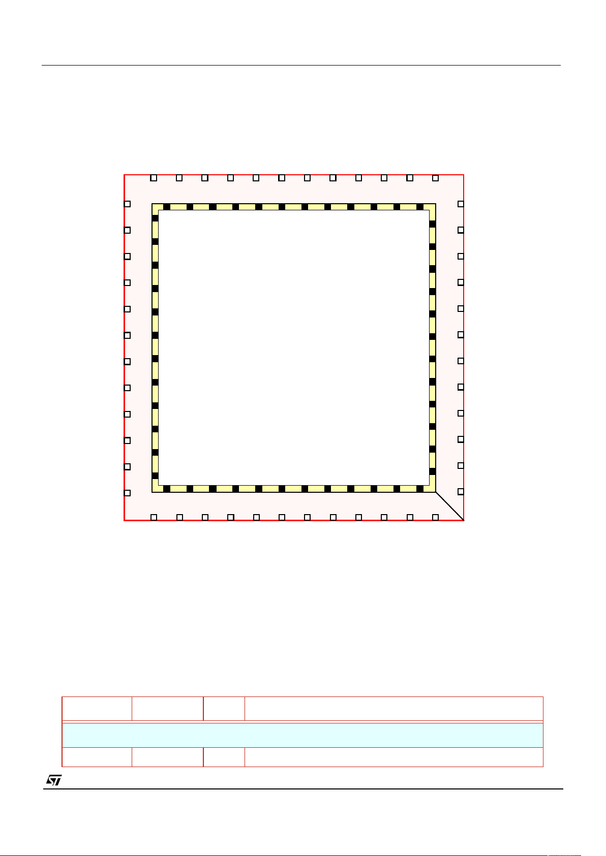
Figure 8 : 48 pin LCC package pin assignment
Name Pin Number Type Description
POWER SUPPLIES
AVSS 11 GND Core analog ground and reference supplies.
RESETB
D[1]
D[2]
D[3]
D[4]
VBASE
VBUS
VBG
VBLOOM
VDDHI
VCMTCAS
NC
OEB
SUSPEND
7
8
6
543214847464544
42
41
38
9
10
11
12
13
14
15
16
17
1920212223242526272829
32
33
34
35
36
37
LST/D[5]
FST/D[6]
CLKI/CLKIP
D[7]
QCK
AUD3V3
AOUTP
40
39
18
30
31
43
VBLTW
D[0]
AOUTN
SDA
PORB
VID3V3
AVSS
AIN
VSSCORE
VSSIO
SCL
VDDIO
NC
NC
NC
NC
NC
NC
NC
SRAMVSS
VRT
NC
NC
CLKIN
NC
REG3V3/VDDCORE
NC
Page 26
STV0672-chipsetf-3-1.fm Pinout and pin descriptions
29 November 2000
Commercial in confidence
26/41
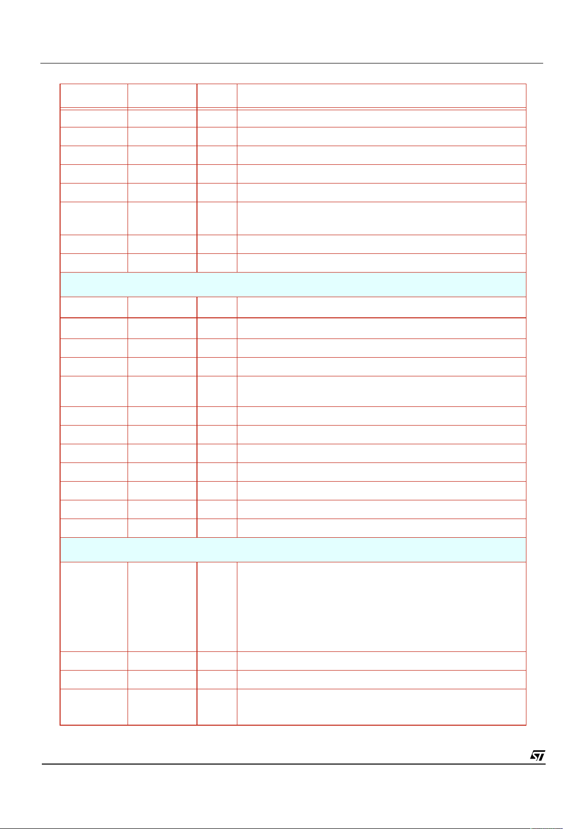
SRAMVSS 21 GND In-column SRAM analog ground.
VDDIO 43 PWR Digital pad ring power.
VSSCORE 29 GND Digital logic ground.
VSSIO 30 GND Digital pad ring ground.
SRAMVSS 21 GND In-column SRAM analogue ground.
VDDCORE/
REG3V3
1
45 PWR Digital logic power/Regulated 3V3 digital supply
VID3V3 12 PWR On-chip Video Supply Voltage Regulator Output
AUD3V3 3 PWR On-chip Audio Amplifier Voltage Regulator Output
ANALOG SIGNALS
VBLOOM
2
8 OA Anti-blooming pixel reset voltage
VBLTW
3
7 OA Bitline test white level reference
VBG 1 OA Internally generated bandgap reference voltage 1.22V
VCMTCAS 13 IA Common-mode input for column pre-amp.
VRT
4
2 IA Pixel reset voltage (nominally a monitor point but can be overdriven
externally)
VDDHI 9 OA Output from voltage doubler, 4.6V -> 4.8V
VBASE 46 OA Drive for base of external bipolar
VBUS 47 IA Incoming power supply 3.3V-> 6V
AIN 4 IA Analog input to Audio Amplifier
AOUTP 5 OA Analog output of Audio Amplifier (positive)
AOUTN 6 OA Analog output of Audio Amplifier (negative)
PORB 16 OA Power-on Reset (Bar) Output.
DIGITAL VIDEO INTERFACE
D[4]
D[3]
D[2]
D[1]
D[0]
36
35
34
33
32
ODT Tri-stateable 5-wire output data bus.
- D[4] is the most significant bit.
- D[4:0] have programmable drive strengths 2, 4 and 6 mA
QCK 42 ODT Tri-stateable data qualification clock.
CLKIN 40 BI↑ LVDS negative Clock input
LST/D[5] 37 ODT Tri-stateable Line start output
May be configured as tri-stateable output data bit 5 D[5].
Name Pin Number Type Description
Page 27
Customer Datasheet, Rev 3.1, 29 November 2000 STV0672-chipsetf-3-1.fm
Commercial in confidence
27/41
29 November 2000
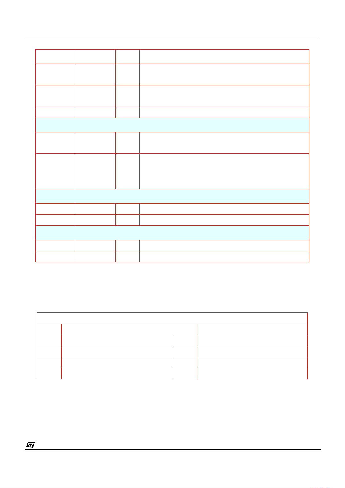
FST/D[6] 38 ODT Tri-stateable Frame start signal.
May be configured as tri-stateable output data bit 6 D[6].
D[7] 41 ODT Tri-stateable Data wire (ms data bit).
May be configured as tri-stateable output data bit 6 D[6].
OEB 20 ID↓ Digital output (tri-state) enable.
DIGITAL CONTROL SIGNALS
RESETB 31 ID↑ System Reset. Active Low.
May be configured as System Sync. Active Low.
SUSPEND 15 ID↑ USB Suspend Mode Control signal. Active High
If this feature is not required then the support circuit must pull the pin to
ground. The combination of an active high signal and pull up pad was
chosen to limit current drawn by the device while in suspend mode.
SERIAL INTERFACE
SCL 18 BI↑ Serial bus clock (input only).
SDA 17 BI↑ Serial bus data (bidirectional, open drain).
SYSTEM CLOCKS
CLKI/CLKIP 39 ID↓ Schmitt Buffered Clock input or LVDS positive Clock input
CLKIN 40 ID↓ LVDS negative Clock input
1. Pre production samples of this device had Reg3V3 and VDDCORE bonded out separately. The production version
of the device will have Reg3V3 and VDDCORE common bonded out to pin 45. There will be no requirement to
change ANY support design/PCB’s as the two signals from pin 44 and pin 45 were connected together on the reference design.
2. Vbloom pin was bonded on pre-production samples but will not be bonded on production parts
3. VBLTW pin was bonded on pre-production samples but will not be bonded on production parts
4. VRT pin was bonded on pre-production samples but will not be bonded on production parts
Key
A Analog Input D Digital Input
OA Analog Output ID↑ Digital input with internal pull-up
BI Bidirectional ID↓ Digital input with internal pull-down
BI↑ Bidirectional with internal pull-up OD Digital Output
BI↓ Bidirectional with internal pull-down ODT Tri-stateable Digital Output
Name Pin Number Type Description
Page 28
STV0672-chipsetf-3-1.fm Pinout and pin descriptions
29 November 2000
Commercial in confidence
28/41
5.3 STV0672 Pin Details
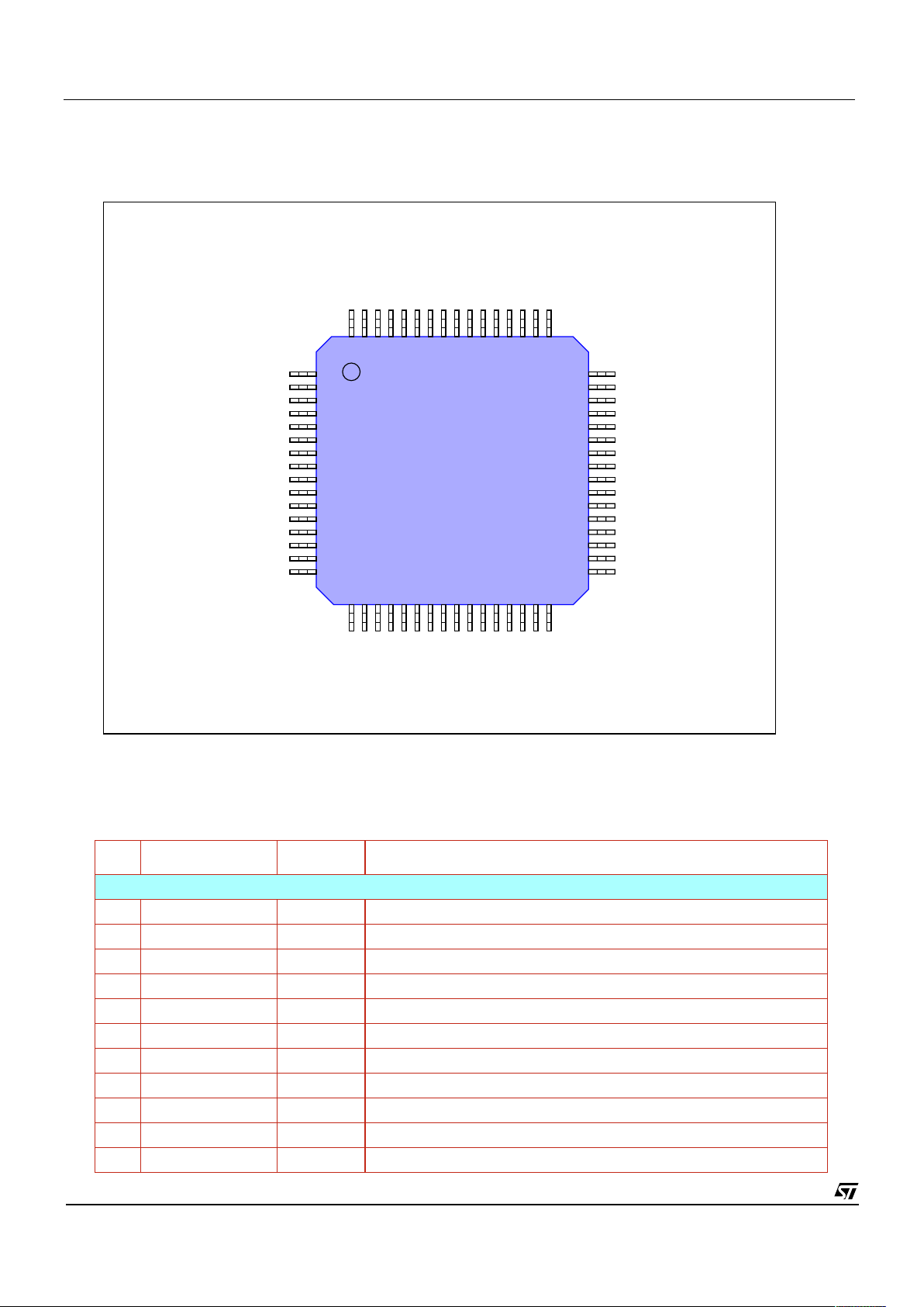
Pin Signal Type
Description
POWER SUPPLIES
1 TEST_CF0 INPUT Test configuration bit - connect to VDD for normal operation
2 TEST_CF1 INPUT Test configuration bit - connect to VDD for normal operation
3 TEST_CF2 INPUT Test configuration bit - connect to VDD for normal operation
4 PLL_VDD INPUT VDD for internal phase locked loop
5 PLL_GND INPUT GND for internal phase locked loop
8 CORE_VDD INPUT VDD for core logic
9 CORE_VSS INPUT Ground for core logic
10 IO_VDD INPUT VDD for pad ring
11 IO_VSS INPUT Ground for pad ring
22 IO_VDD INPUT VDD for pad ring
23 IO_VSS INPUT Ground for pad ring
MICROPORT_5
MICROPORT_3
MICROPORT_2
MICROPORT_1
MICROPORT_0
IO_VDD
SWITCH_INT_N
IO_VDD
CORE_GND
TEST_CONF1
USB_DP
EEPROM_SDA
EEPROM_SCL
USB_DN
PLL_VDD
PLL_GND
XTAL_IN
XTAL_OUT
CORE_GND
IO_VDD
IO_GND
DIGIPORT_9
RESET_N
MICROPORT_7
MICROPORT_6
MICROPORT_4
IO_GND
MICROPORT_12
XXXX_INT_N
SSDA
SSCL
IO_GND
DIGIPORT_5
CORE_VDD
TEST_CONF0
TEST_CONF2
SPDN
CORE_VDD
MICROPORT_11
IO_GND
MICROPORT_9
MICROPORT_8
DIGIPORT_7
DIGIPORT_8
DIGIPORT_6
MICROPORT_14
MICROPORT_13
MICROPORT_10
DIGIPORT_4
DIGIPORT_3
DIGIPORT_2
DIGIPORT_1
DIGIPORT_0
IO_VDD
IO_GND
CORE_VDD
CORE_GND
SENSOR_CLK
SENSOR_DB5
SENSOR_DB4
SENSOR_DB3
SENSOR_DB2
SENSOR_DB1
SENSOR_DB0
1
17
16
32
33
48
4964
Figure 9 : CPIA 2 Pinout - Packaged in 64 TQFP
Page 29
Customer Datasheet, Rev 3.1, 29 November 2000 STV0672-chipsetf-3-1.fm
Commercial in confidence
29/41
29 November 2000
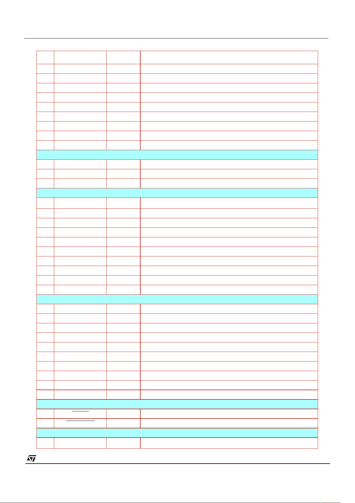
24 CORE_VDD INPUT VDD for core logic
25 CORE_VSS INPUT Ground for core logic
39 IO_VDD INPUT VDD for pad ring
40 IO_VSS INPUT Ground for pad ring
49 IO_VSS INPUT Ground for pad ring
57 CORE_VDD INPUT VDD for core logic
58 CORE_VSS INPUT Ground for core logic
59 IO_VDD INPUT VDD for pad ring
60 IO_VSS INPUT Ground for pad ring
DEVICE MASTER CLOCK AND RESET
6 XTAL_IN ANA System clock pad
7 XTAL_OUT OSC System clock pad
33 RESET_N SCHMITT System, power-on-reset supplied by companion sensor
DIGIPORT/USB CONFIG INTERFACE
12
DIGIPORT_9
1
BIDIR unused (leave unconnected)
2
13 DIGIPORT_8 BIDIR unused (connect to VSS)
14 DIGIPORT_7 BIDIR Programmable USB vendor ID
15 DIGIPORT_6 BIDIR Programmable USB vendor ID
16 DIGIPORT_5 BIDIR Programmable USB vendor ID
17 DIGIPORT_4 BIDIR Programmable USB vendor ID
18 DIGIPORT_3 BIDIR Programmable USB vendor ID
19 DIGIPORT_2 BIDIR Programmable USB vendor ID
20 DIGIPORT_1 BIDIR Programmable USB vendor ID
21 DIGIPORT_0 BIDIR Programmable USB vendor ID
SENSOR INTERFACE
26 SENSOR_CLK BIDIR
VV6410/VV6500 Sensor Clock
27 SENSOR_DB5 BIDIR
VV6410/VV6500 Sensor Data Bus [bit5]
28 SENSOR_DB4 BIDIR
VV6410/VV6500 Sensor Data Bus [bit4]
29 SENSOR_DB3 BIDIR
VV6410/VV6500 Sensor Data Bus [bit3]
30 SENSOR_DB2 BIDIR
VV6410/VV6500 Sensor Data Bus [bit2]
31 SENSOR_DB1 BIDIR
VV6410/VV6500 Sensor Data Bus [bit1]
32 SENSOR_DB0 BIDIR
VV6410/VV6500 Sensor Data Bus [bit0]
34 SSDA 3 state
VV6410/VV6500 Sensor Serial Interface Data
35 SSCL 3 state
VV6410/VV6500 Sensor Serial Interface Clock
36 SPDN BIDIR
Control line to sensor to select ultra low power SUSPEND mode
MISC CONTROL
37 XX_INT INPUT
Remote wakeup
38 SWITCH_INT INPUT
Load TWAIN driver data upload
MICROPORT/GPIO INTERFACE
41
MICROPORT_0
3
BIDIR General Purpose Input/Output (GPIO)
Pin Signal Type Description
Page 30
STV0672-chipsetf-3-1.fm Pinout and pin descriptions
29 November 2000
Commercial in confidence
30/41
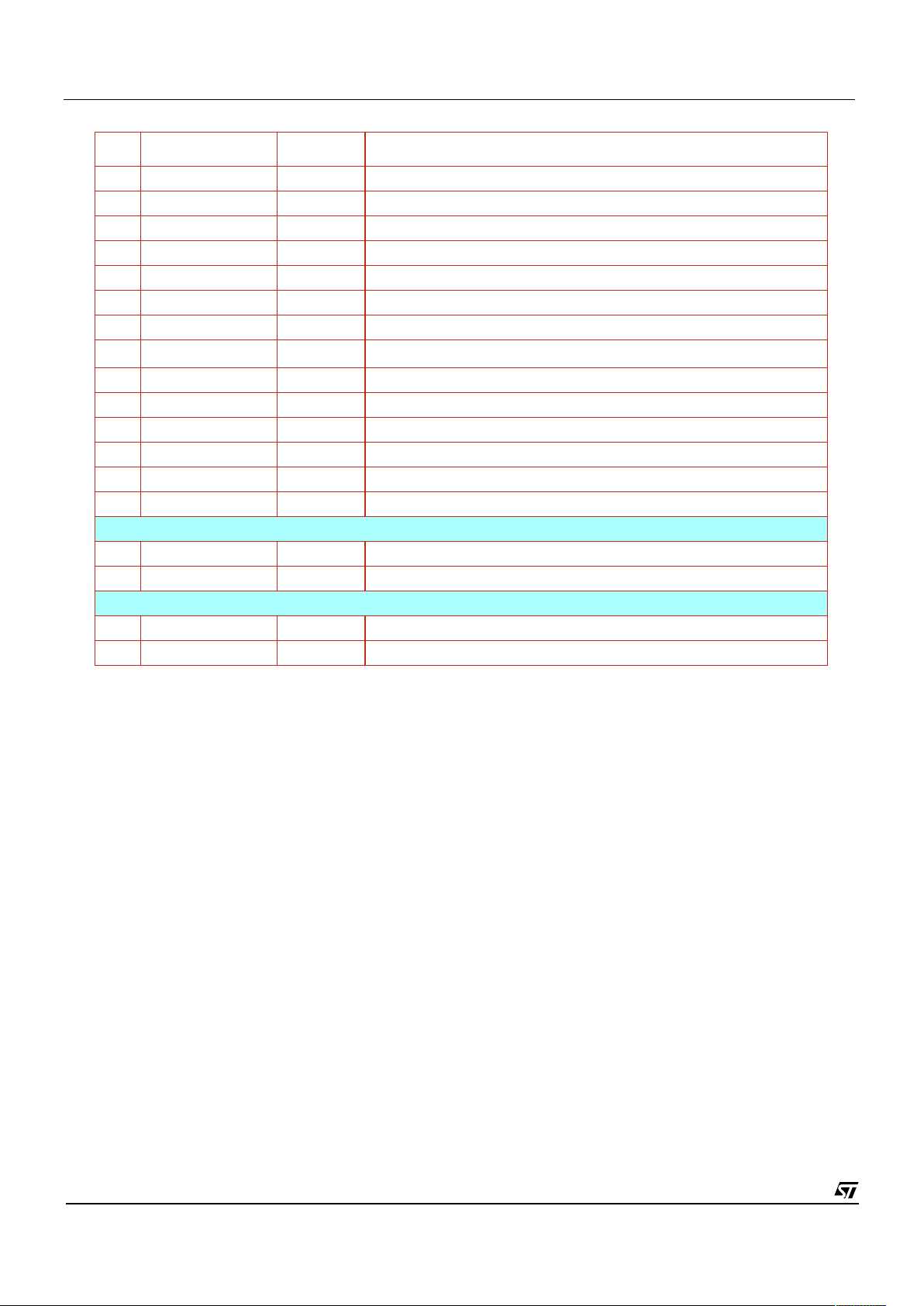
42 MICROPORT_1 BIDIR General Purpose Input/Output (GPIO)
43 MICROPORT_2 BIDIR General Purpose Input/Output (GPIO)
44 MICROPORT_3 BIDIR General Purpose Input/Output (GPIO)
45 MICROPORT_4 BIDIR General Purpose Input/Output (GPIO)
46 MICROPORT_5 BIDIR General Purpose Input/Output (GPIO)
47 MICROPORT_6 BIDIR General Purpose Input/Output (GPIO)
48 MICROPORT_7 BIDIR General Purpose Input/Output (GPIO)
50
MICROPORT_8
4
BIDIR VDD
51 MICROPORT_9 BIDIR VSS
52 MICROPORT_10 BIDIR VDD
53 MICROPORT_11 BIDIR VDD
54 MICROPORT_12 BIDIR VDD
55 MICROPORT_13 BIDIR VSS
56 MICROPORT_14 BIDIR VSS
USB INTERFACE
61 USB_DN BIDIR USB data line
62 USB_DP BIDIR USB data line
EEPROM INTERFACE
63 EEPROM_SDA BIDIR Serial data to/from the EEPROM
64 EEPROM_SCL OUTPUT Serial clock to the EEPROM
1. The DIGIPORT pins can be reconfigured, please contact STMicroelectronics for more details on this feature
2. Bit[9] of the DIGIPORT is connected to VDD in current Reference Design. This is incorrect and should be left
unconnected to ensure that no extra supply current is drawn.
3. The MICROPORT bus can be reconfigured, please contact STMicroelectronics for more details on this feature
4. Bit8 of the MICROPORT can enable extra device functionality, please contact STMicroelectronics for more details
on this feature.
Pin Signal Type Description
Page 31
Customer Datasheet, Rev 3.1, 29 November 2000 STV0672-chipsetf-3-1.fm
Commercial in confidence
31/41
29 November 2000
6. Package Details
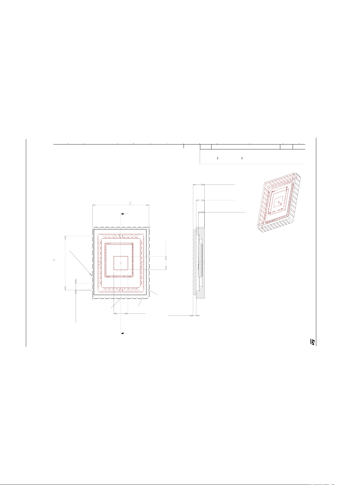
6.1 VV6410 (36pin CLCC)
RevNo
Revision note
Date
2
1
3
4
5
6
78
ECN No.
10.67 - 0.13
+0.30
2.67
2.02
8.13 0.13
1.02 0.13
40 Places
R
0.15
Notes.
1. Die is optically centred.
2. Refractive index of glass is ~1.52.
3. Distance to optical surface of Die.
4. Pixel area of sensor.
Pin 1
Pin 5
Pin 6
A
A
1.16 0.09 (note 3)
2.15 -0.26
+0.16
0.60 -0.10
0.00
1.55 0.16
A-A (8 : 1)
A Pin Locations changed, tolerance added to O/all dims 14/7/99
B Package now 36 Pin 20/7/99
C 1.03 0.13 was 1.03 0.08 2/8/99
D 1.16 dim tolerance revised 15/10/99
Page 32
STV0672-chipsetf-3-1.fm Package Details
29 November 2000
Commercial in confidence
32/41
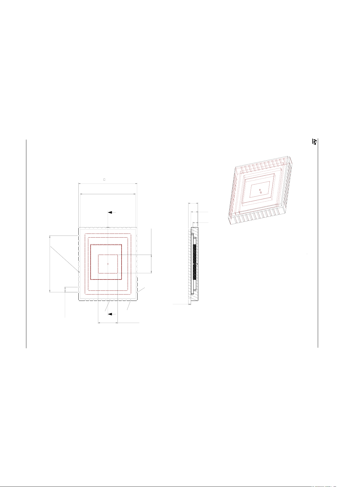
6.2 VV6500 (48pin CLCC)
14.52
14.09
4.83 (note 4)
3.63
(Note 4)
R
0.15
, 48 Places
11.18 0.13
1.02 0.13
13.70
Not
es.
1. Die is optically centred.
2. Refractive index of glass is ~1.52.
3. Distance to optical surface of Die.
4. Pixel area of sensor.
Pin 1
Pin 6
Pin 7
A
A
2.34
1.91
1.71
1.39
1.21
1.09
0.60
0.50
A-A
Page 33
Customer Datasheet, Rev 3.1, 29 November 2000 STV0672-chipsetf-3-1.fm
Commercial in confidence
33/41
29 November 2000
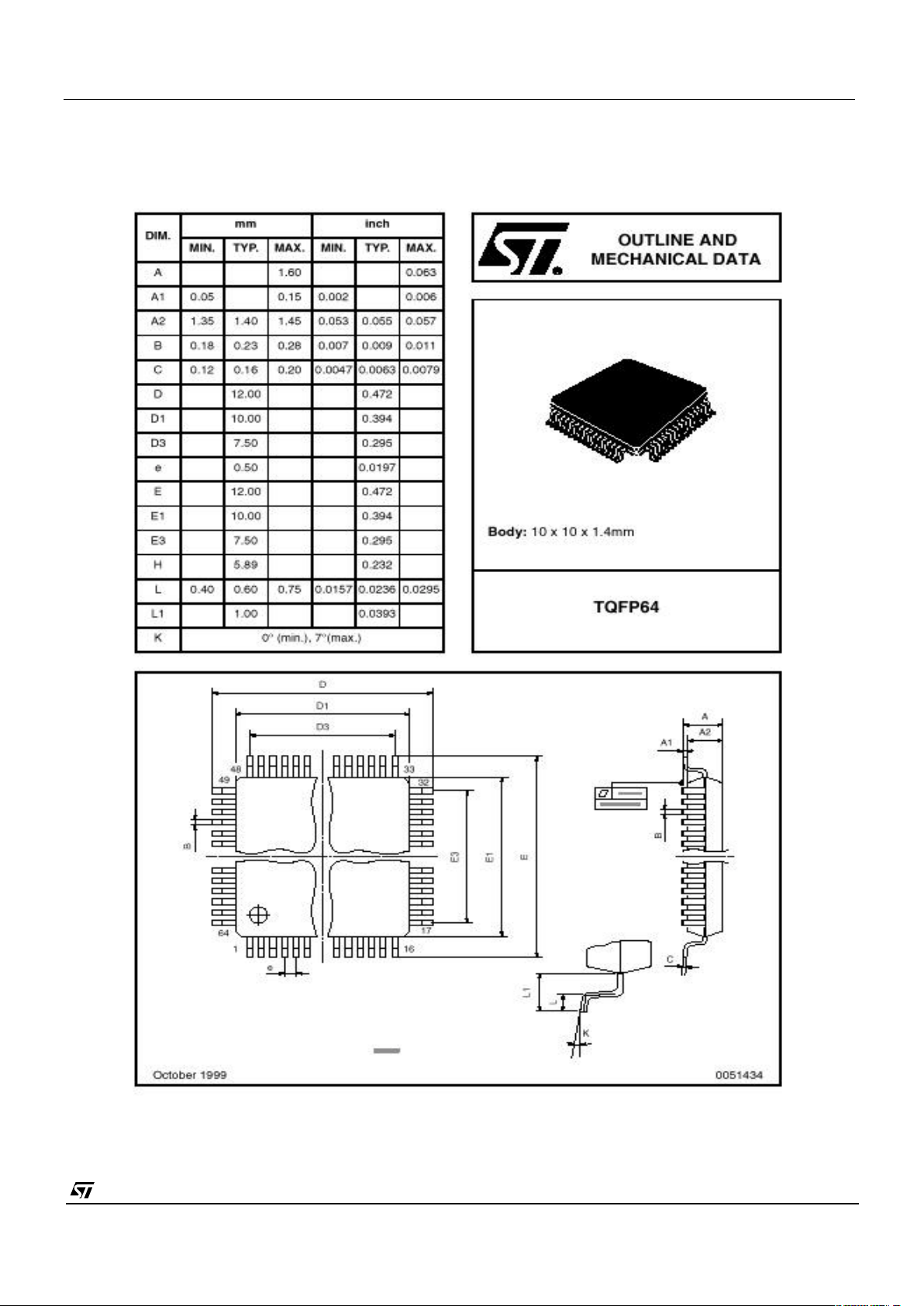
6.3 STV0672 (64pin TQFP)
Figure 10 : STV0672 package details
Page 34
STV0672-chipsetf-3-1.fm VV6410/VV6500+STV0672 Reference Design
29 November 2000
Commercial in confidence
34/41
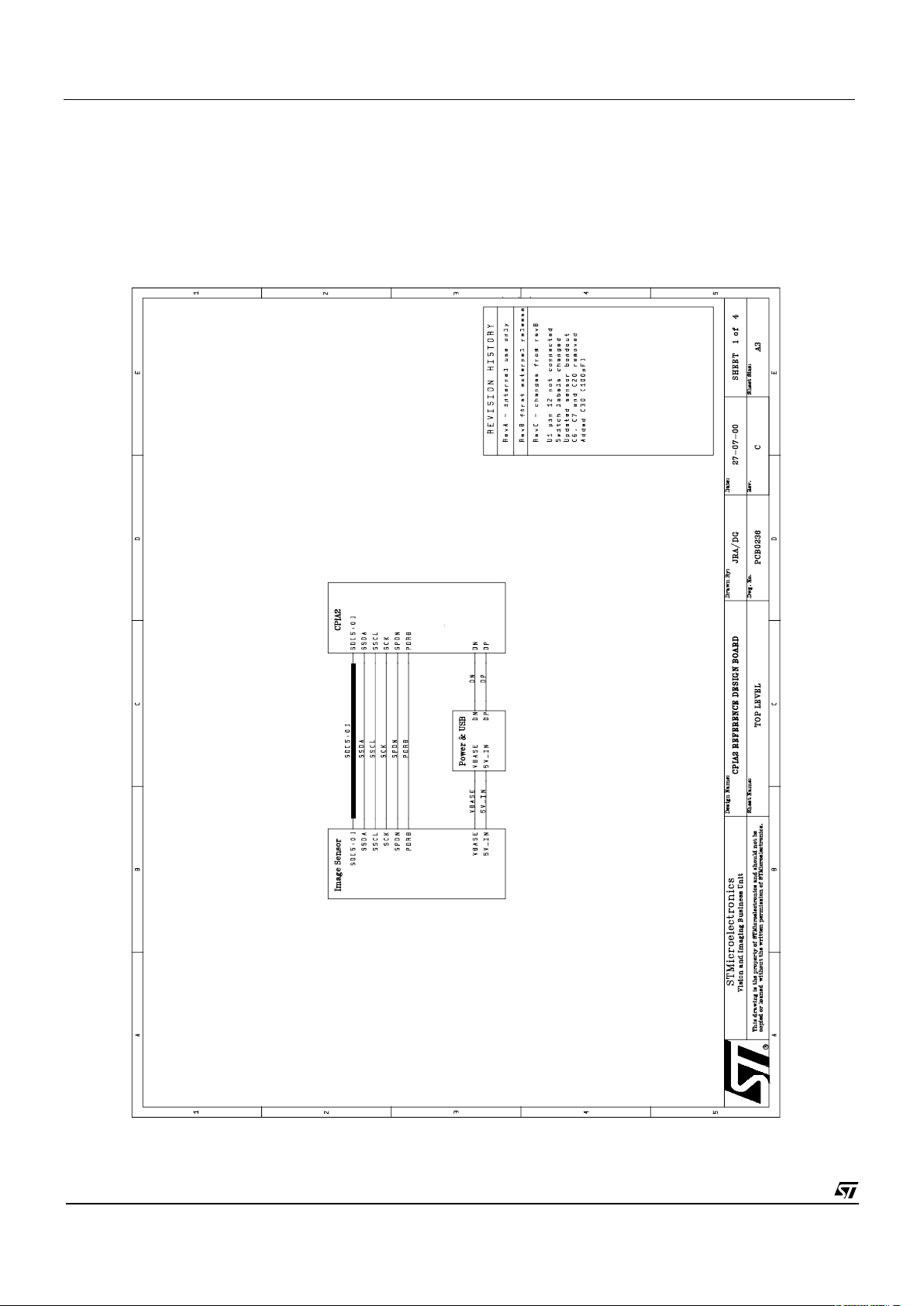
7. VV6410/VV6500+STV0672 Reference Design
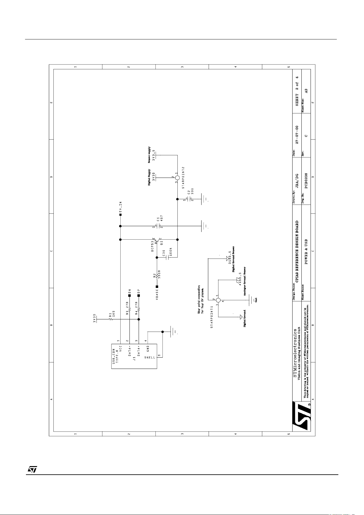
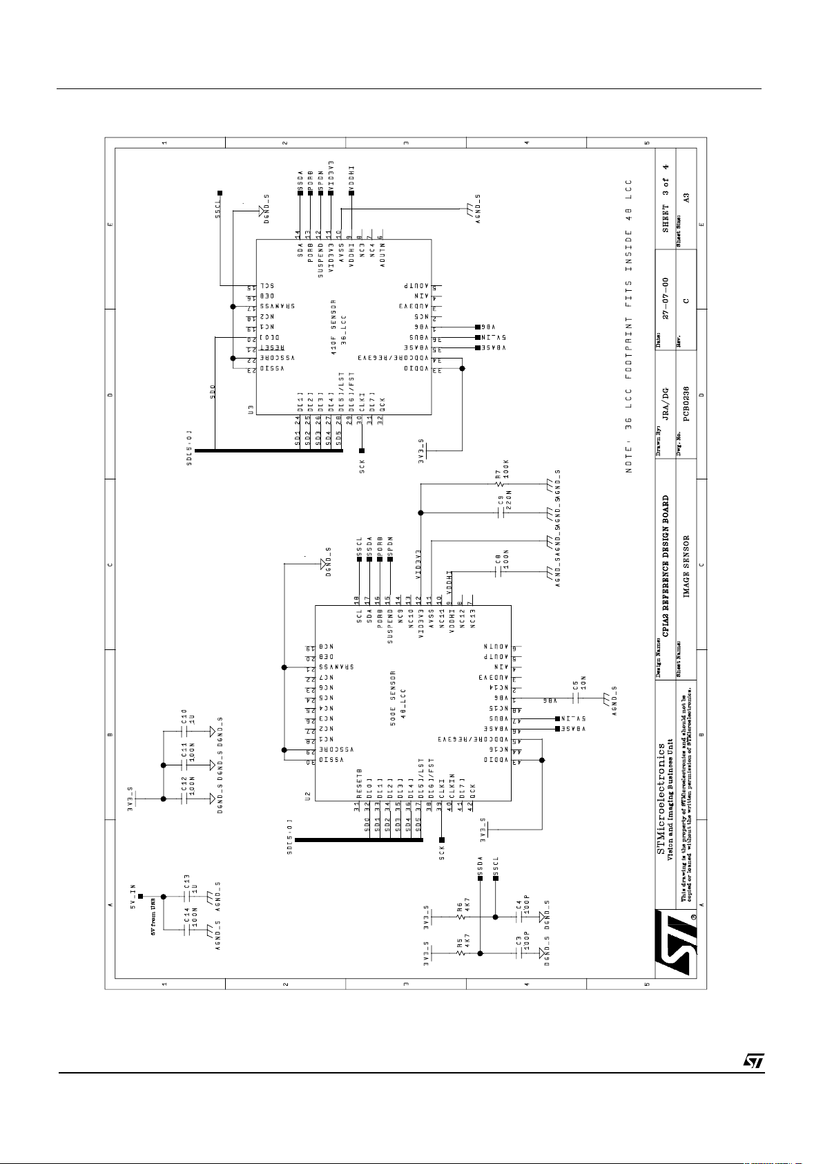
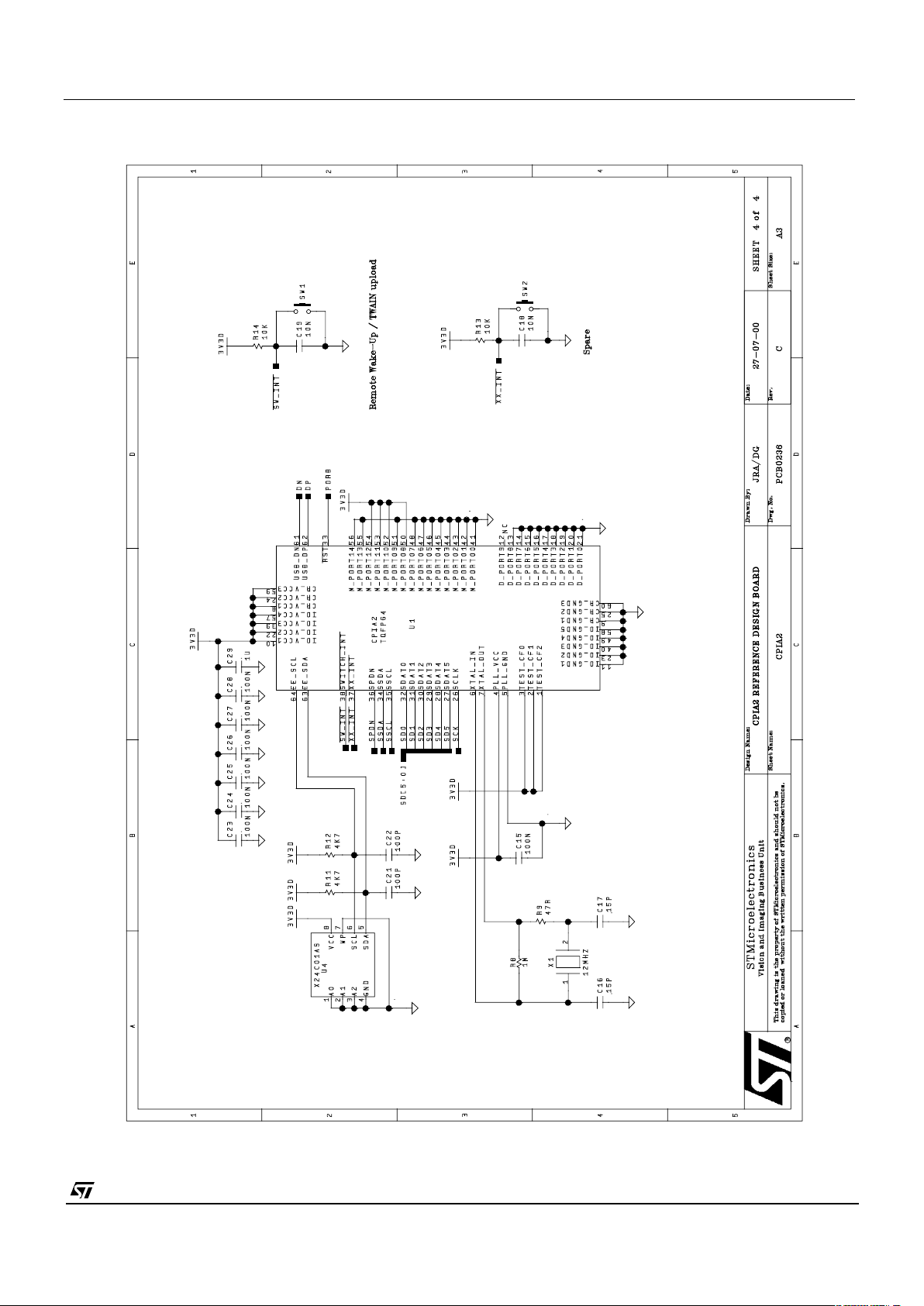
STMicroelectronics will make a reference design available for the VV6410/VV6500+STV0672 chipset. Contact
STMicroelectronics for more details.
The schematics describing the reference design are included over the following 4 pages of the datasheet
Page 35
Customer Datasheet, Rev 3.1, 29 November 2000 STV0672-chipsetf-3-1.fm
Commercial in confidence
35/41
29 November 2000
Page 36
STV0672-chipsetf-3-1.fm VV6410/VV6500+STV0672 Reference Design
29 November 2000
Commercial in confidence
36/41
Page 37
Customer Datasheet, Rev 3.1, 29 November 2000 STV0672-chipsetf-3-1.fm
Commercial in confidence
37/41
29 November 2000
Page 38

STV0672-chipsetf-3-1.fm Reference Design and Evaluation Kits (RDK’s and EVK’s)
29 November 2000
Commercial in confidence
38/41
8. Reference Design and Evaluation Kits (RDK’s and EVK’s)
STMicroelectronics supply a full range of supporting reference design kits for their range of sensors and coprocessors. The STVUSB /VGA-R01 (comprising the STV0672 coprocessor and the 6500 VGA resolution sensor) and STV-USB/CIF-R01 (comprising
the STV0672 coprocessor and the 6410 CIF resolution sensor) reference design kits allow direct interface to a PC via the USB
port.
A full Evaluation Kit for the USB camera chipset will also be available in the future. Please contact STMicroelectronics for more
details on this product.
Please contact STMicroelectronics for more details on how to order these support products.
Page 39

Customer Datasheet, Rev 3.1, 29 November 2000 STV0672-chipsetf-3-1.fm
Commercial in confidence
39/41
29 November 2000
9. Design Issues
The PCB gerbers that are included in the documentation package that accompanies the Reference Design Kit shows the sensor
and the coprocessor onthe same side of the PCB. Although this placement of the IC’s will not give the smallest physical design it
will avoid any excess heatbeing transferred from STV0672 to the sensors. Excess heat in the sensor isa source of noise that will
degrade the image performance, especially in low light.
STMicroelectronics therefore recommends that the “side-by-side” orientation of STV0672 and 6410/6500 should be followed if
the design is to achieve optimal image performance under a wide range of lighting conditions.
Page 40

STV0672-chipsetf-3-1.fm Ordering Details
29 November 2000
Commercial in confidence
40/41
10. Ordering Details
For more information on the appropriate sensor choice please contact STMicroelectronics.
Part number Description
VV6410C036 CIF image sensor, 36CLCC Package
VV6500C001 VGA image sensor, 48CLCC Package
STV0672 Companion USB co-processor
STV-USB/CIF-R01 USB chipset, CIF resolution reference design kit
STV-USB/VGA-R01 USB chipset, VGA resolution reference design kit
Table 15 : Ordering details
Page 41

Commercial in confidence
41/41
Information furnished is believed to be accurate and reliable. However, STMicroelectronics assumes no responsibility for the
consequences of use of such information nor for any infringement of patents or other rights of third parties which may result from
its use. No license is granted by implication or otherwise under any patent or patent rights of STMicroelectronics. Specifications
mentioned in this publication are subject to change without notice. This publication supersedes and replaces all information
previously supplied. STMicroelectronics products are not authorized for use as critical components in life support devices or
systems without express written approval of STMicroelectronics
The ST logo is a registered trademark of STMicroelectronics
© 2000 STMicroelectronics - All Rights Reserved
Imaging Divison
29 November 2000
Customer Datasheet, Rev 3.1, 29 November 2000 STV0672-chipsetf-3-1.fm
www.st.com
 Loading...