

Page 1
STV9553
12 ns TRIPLE-CHANNEL HIGH VOLTAGE VIDEO AMPLIFIER
FEATURES
■ Triple-channel video amplifier
■ Supply voltage up to 115 V
■ 80V Output dynamic range
■ Perfect for PICTURE BOOST application
requiring high video amplitude
■ Pinning for easy PCB layout
■ Supports DC coupling (optimum cost saving)
and AC coupling applications.
■ Built-in Voltage Gain: 20 (Typ.)
■ Rise and Fall Times: 12 ns (Typ.)
■ Bandwidth: 29 MHz (Typ.)
■ Very low stand-by power consumption
■ Perfectly matched with the STV921x
preamplifiers
DESCRIPTION
The STV9553 is a triple-channel video amplifier
designed in a 120V-high voltage technology and
able to drive in DC-coupling mode the 3 cathodes
of a CRT monitor.
The STV9553 supports PICTURE BOOST
applications where video amplitude up to 50V or
above is required, ensuring a maximum quality of
the still pictures or moving video.
Perfecly matched with the STV921x ST
preamplifiers, it provides a highly performant and
very cost effective video system.
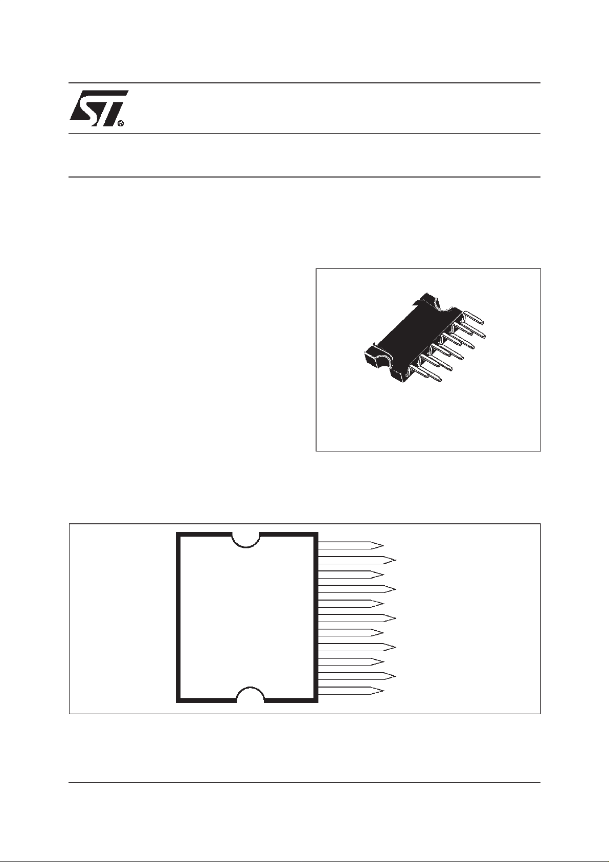
CLIPWATT 11
(Plastic Package)
ORDER CODE: STV9553
PIN CONNECTIONS
11
10
9
8
7
6
5
4
3
2
1
February 2002 1/24
OUT1
OUT2
OUT3
GNDP
V
DD
GNDS
GNDA
IN3
V
CC
IN2
IN1
Version 4.0
1
Page 2

Table of Contents
1 BLOCK DIAGRAM . . . . . . . . . . . . . . . . . . . . . . . . . . . . . . . . . . . . . . . . . . . . . . . . . . . . . . . . . . . 3
2 PIN DESCRIPTION . . ........................................................ 3
3 ABSOLUTE MAXIMUM RATINGS . . . . . . . . . . . . . . . . . . . . . . . . . . . . . . . . . . . . . . . . . . . . . . 4
4 THERMAL DATA . . . . . . . . . . . . . . . . . . . . . . . . . . . . . . . . . . . . . . . . . . . . . . . . . . . . . . . . . . . . 4
5 ELECTRICAL CHARACTERISTICS . . . . . . . . . . . . . . . . . . . . . . . . . . . . . . . . . . . . . . . . . . . . . 5
6 THEORY OF OPERATION . . . . . . . . . . . . . . . . . . . . . . . . . . . . . . . . . . . . . . . . . . . . . . . . . . . . 7
6.1 General . . . . . . . . . . . . . . . . . . . . . . . . . . . . . . . . . . . . . . . . . . . . .................7
6.2 Output voltage . . . . . . . . . . . . . . . . . . . . .................................... 8
7 POWER DISSIPATION . . . . . . . . . . . . . . . . . . . . . . . . . . . . . . . . . . . . . . . . . . . . . . . . . . . . . . . 9
8 TYPICAL PERFORMANCE CHARACTERISTICS . . . . . . . . . . . . . . . . . . . . . . . . . . ....... 10
9 INTERNAL SCHEMATICS . . . . . . . . . . . . . . . . . . . . . . . . . . . . . . . . . . . . . . . . . . . . . . . . . . . . 11
10 APPLICATION HINTS . . . . . . . . . . . . . . . . . . . . . . . . . . . . . . . . . . . . . . . . . . . . . . . . . . . . . . . 12
10.1 How to choose the high supply voltage value (VDD) in DC coupling mode . . . . . . . . 12
10.2 Arcing Protection: schematics . . . . ....................................... 12
10.3 Arcing protection: layout and decoupling . . . ................................ 13
10.4 Video response optimization: schematics in DC-coupling mode . . . . . . . . . . . . . . . . . 14
10.5 Video response optimization: outputs networks . . . . . . . . . . . . . . . . . . . . . . . . . . . . . . 15
10.6 Video response optimization: inputs networks . . . . . . . . . . . . . . . . . . . . . . . . . . . . . . . 15
10.7 Video response optimization: layout and decoupling . . . . . . . . . . . .. . . . . . . . . . . . . . 15
10.8 AC - Coupling mode . . . . . . . . . . . . . . . . . . . . . . . . . . . . . . . . . . . ................ 16
10.9 Stand-by mode, spot suppression . . . . . . . . . . . . . . . . . . . . . . . . . . . . . . . . . . . . . . . . 17
10.10 Conclusion . . . . . . . . . . . . . . . . . . . ....................................... 18
11 PACKAGE MECHANICAL DATA . . . . . . . . . . . . . . . . . . . . . . . . . . . . . . . . . . . . . . . . . . . . . . 22
2/24
2
2
Page 3
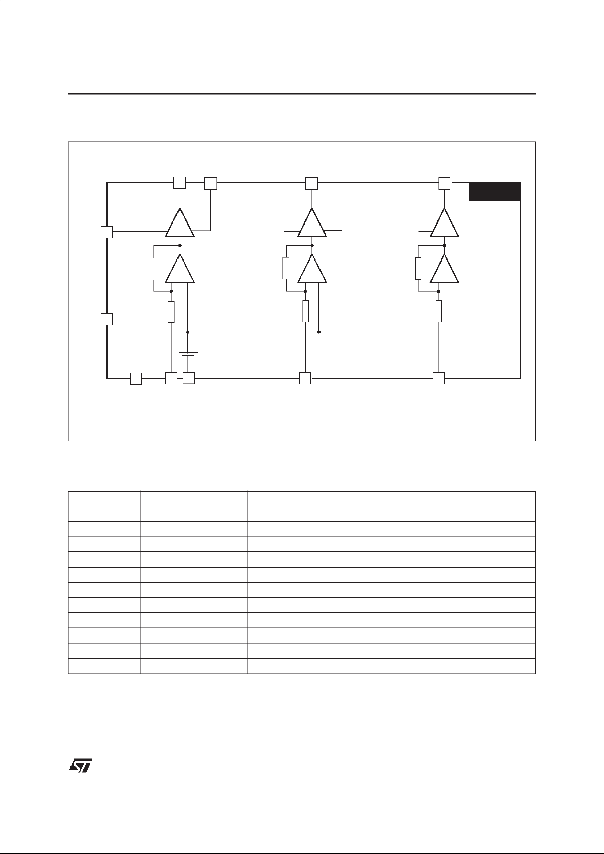
1 BLOCK DIAGRAM
STV9553
VDD
VCC
OUT1
108
OUT3GNDP OUT2
911
STV9553
VDD GNDP
7
3
V
REF
6
5
1
2
VDD GNDP
4
IN3IN2IN1 GNDAGNDS
2 PIN DESCRIPTION
Pin Name Function
1 IN1 Video Input (channel 1)
2 IN2 Video Input (channel 2)
3 VCC Low Supply Voltage
4 IN3 Video Input (channel 3)
5 GNDA Ground Analog
6 GNDS Ground Substrat
7 VDD High Supply Voltage
8 GNDP Ground Power
9 OUT3 Video output (channel 3)
10 OUT2 Video output (channel 2)
11 OUT1 VIdeo output (channel 1)
3/24
3
Page 4

STV9553
3 ABSOLUTE MAXIMUM RATINGS
Symbol Parameter Value Unit
V
V
V
I
I
V
IN Max
V
IN Min
T
DD
CC
ESD
OD
OG
T
J
STG
High supply voltage 120 V
Low supply voltage 16.5 V
ESD susceptibility
Human Body Model (100pF discharged through 1.5KΩ)
EIAJ norm (200pF discharged through 0Ω)
2
300
Output source current (pulsed < 50µs) 80 mA
Output sink current (pulsed < 50µs) 80 mA
Maximum Input Voltage VCC+0.3 V
Minimum Input Voltage - 0.5 V
Junction Temperature 150 °C
Storage Temperature -20 + 150 °C
kV
V
4 THERMAL DATA
Symbol Parameter Value Unit
R
th (j-c)
R
th (j-a)
Junction-Case Thermal Resistance (Max.) 3 °C/W
Junction-Ambient Thermal Resistance (Typ.) 35 °C/W
4/24
3
Page 5
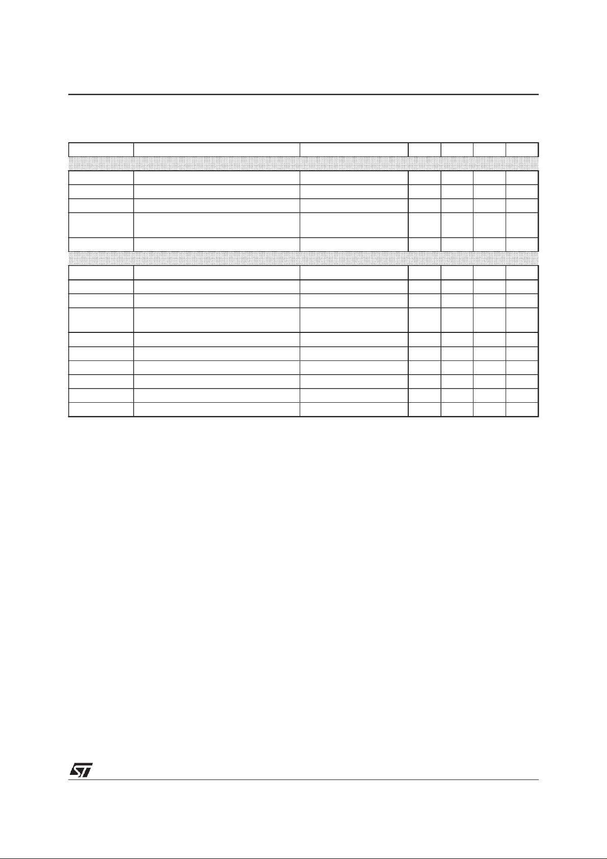
5 ELECTRICAL CHARACTERISTICS
Symbol Parameter Test Conditions Min. Typ Max Unit
SUPPLY parameters (V
V
V
I
DD
I
DDS
I
CC
DD
CC
High supply voltage 20 110 115 V
Low supply voltage 10 12 15 V
VDDsupply current V
VDDstand-by supply current
VCCsupply current V
STATIC parameters (V
DC output voltage VIN=1.90 V 77 80 83 V
High voltage supply rejection V
DD
/dT Output voltage drift versus temperature V
Output voltage matching versus
/dT
temperature (Note 2)
Video input resistor V
Output saturation voltage to supply I0= -60mA (Note 3) V
Output saturation voltage to GND I0= 60mA (Note 3) 11 V
dV
d∆V
dV
V
OUT
OUT
R
V
V
OUT
/dV
OUT
IN
SATH
SATL
G Video Gain V
LE Linearity Error 17 V<V
V
REF
Internal voltage reference 5.6 V
= 12V, VDD= 110V, Tamb = 25 °C, unless otherwise specified)
CC
= 50V 15 mA
OUT
V
: switched off (<1.5V)
CC
: low (Note 1)
V
OUT
= 50V 40 mA
OUT
= 12V, VDD= 110V, Tamb = 25 °C)
CC
=50V 0.5 %
OUT
= 80V 15 mV/°C
OUT
V
= 80V 1 mV/°C
OUT
=50V 2 kΩ
OUT
= 50V 20
OUT
OUT<VDD
-15 V 3 8 %
60 µA
-6.5 V
DD
STV9553
Note 1: The STV9553 goes into stand-by mode when Vcc is switched off (<1.5V).
In stand-by mode, Vout is set to low level.
Note 2: Matching measured between each channel.
Note 3: Pulsed current width < 50µs
5/24
3
Page 6
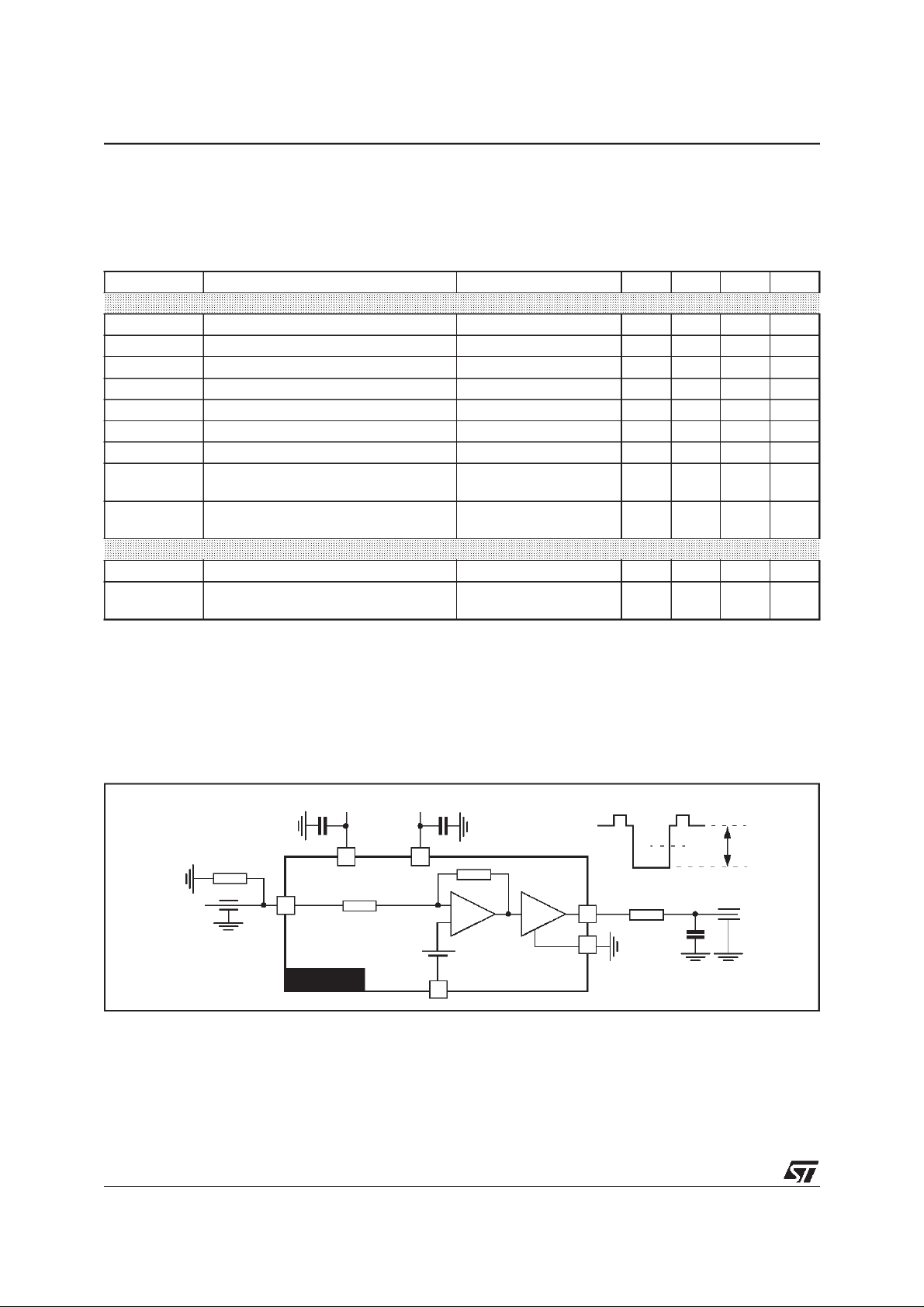
STV9553
ELECTRICAL CHARACTERISTICS (continued)
Symbol Parameter Test Conditions Min. Typ Max Unit
DYNAMIC parameters (see Figure 1)
t
R
t
F
OS
R
OS
F
∆G Low frequency gain matching (Note 4) V
BW Bandwidth at -3dB V
t
SET
CT
L
CT
H
Rise time VDC=50V, ∆V=40V
Fall time VDC=50V, ∆V=40V
PP
PP
Overshoot, white to black transition 5 %
Overshoot, black to white transition 0 %
= 50V, f=1MHz 5 %
DC
=50V, ∆V=20V
DC
2.5% Settling time VDC=50V, ∆V=40V
V
=50V, ∆V=20V
Low frequency crosstalk
High frequency crosstalk
DC
f = 1 MHz 50 dB
V
=50V, ∆V=20V
DC
f = 20MHz 32 dB
PP
PP
PP
PP
DYNAMIC parameter in PICTURE BOOST condition (Note 5)
t
OS
PB
PB
Rise/fall time VDC=50V, ∆V=60V
Overshoot white to black or black to white
transition
=50V, ∆V=60V
V
DC
PP
PP
Note 4: Matching measured between each channel.
Note 5: PICTURE BOOST condition (video amplitude at 50V or above) is used in some applications when displaying
still picture or moving video. In this condition the high level of contrast improves the pictures quality at the
expense of the video performances (t
and Overshoot) which are slightly deteriorated.
R,tF
10.8 ns
12.8 ns
29 MHz
15 ns
15 ns
9%
Figure 1. AC test circuit
50Ω
IN
6/24
3
V
CC
1
STV9553
110V12V
V
3
DD
7
∆V
V
DC
OUT RP= 300 Ω
11
CL=8pF
V
REF
8
GNDP
5
GNDA
Page 7
STV9553
6 THEORY OF OPERATION
6.1 General
The STV9553 is a three-channel video amplifier supplied by a low supply voltage: VCC(typ.12V) and a
high supply voltage: VDD(up to 115V).
The high values of VDDsupplying theamplifier output stage allow direct control of the CRT cathodes (DC
coupling mode).
In DC coupling mode, the application schematic is very simple and only a few external components are
needed to drive the cathodes. In particular, there is no need of the DC-restore circuitry which is used in
classical AC coupling applications.
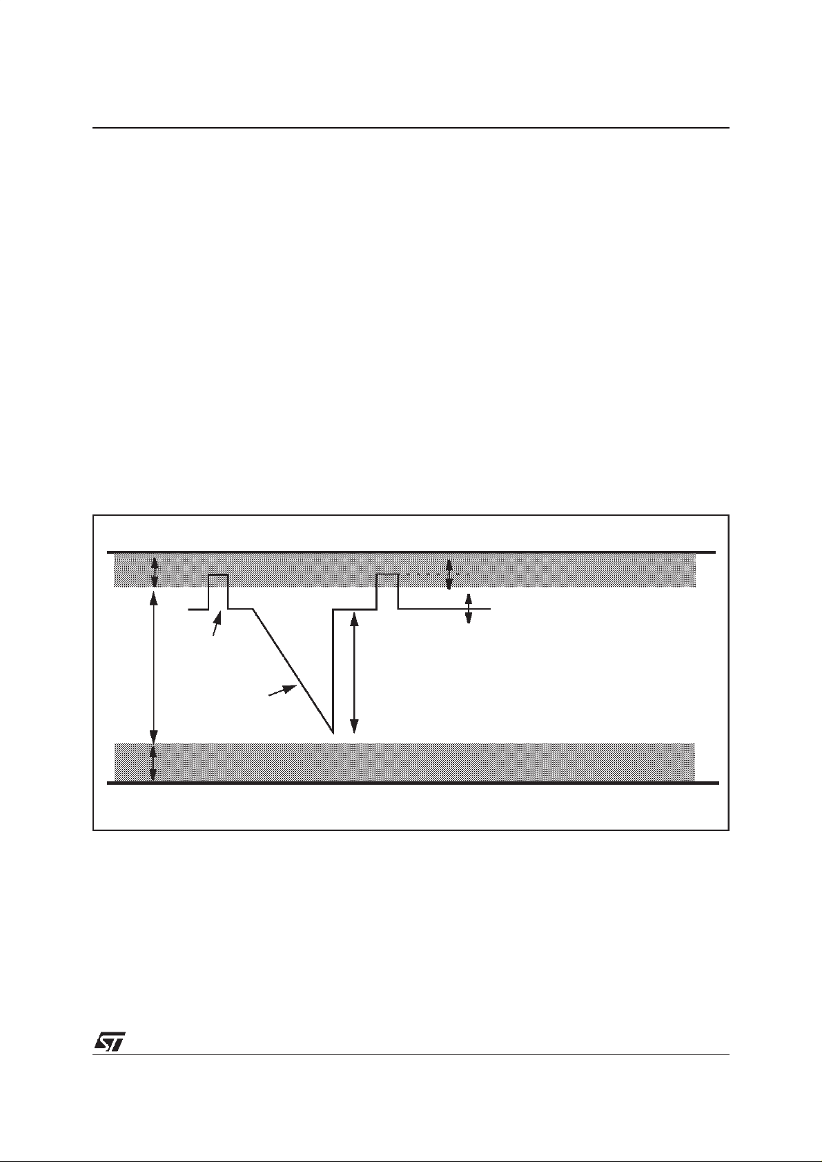
The output voltage range is wide enough (Figure 2) to provide simultaneously :
– Cut-off adjustment (typ. 25V)
– Video contrast (typ. up to 40V),
– Brightness (with the remaining voltagerange).
In normal operation, the output video signal must remain inside the linear region whatever the cut-off,
brightness and contrast adjustments are.
Figure 2. Output signal, level adjustments
15V
17V
V
DD
(A) Top Non-Linear Region
Blanking pulse
Linear region
GND
Video Signal
(E) Bottom Non-Linear Region
(B) Cut-off Adjust. (25V Typ.)
(C) Brightness Adjust. (10V Typ.)
(D) Contrast Adjust. (40V Typ.)
7/24
3
Page 8
STV9553
6.2 Output voltage
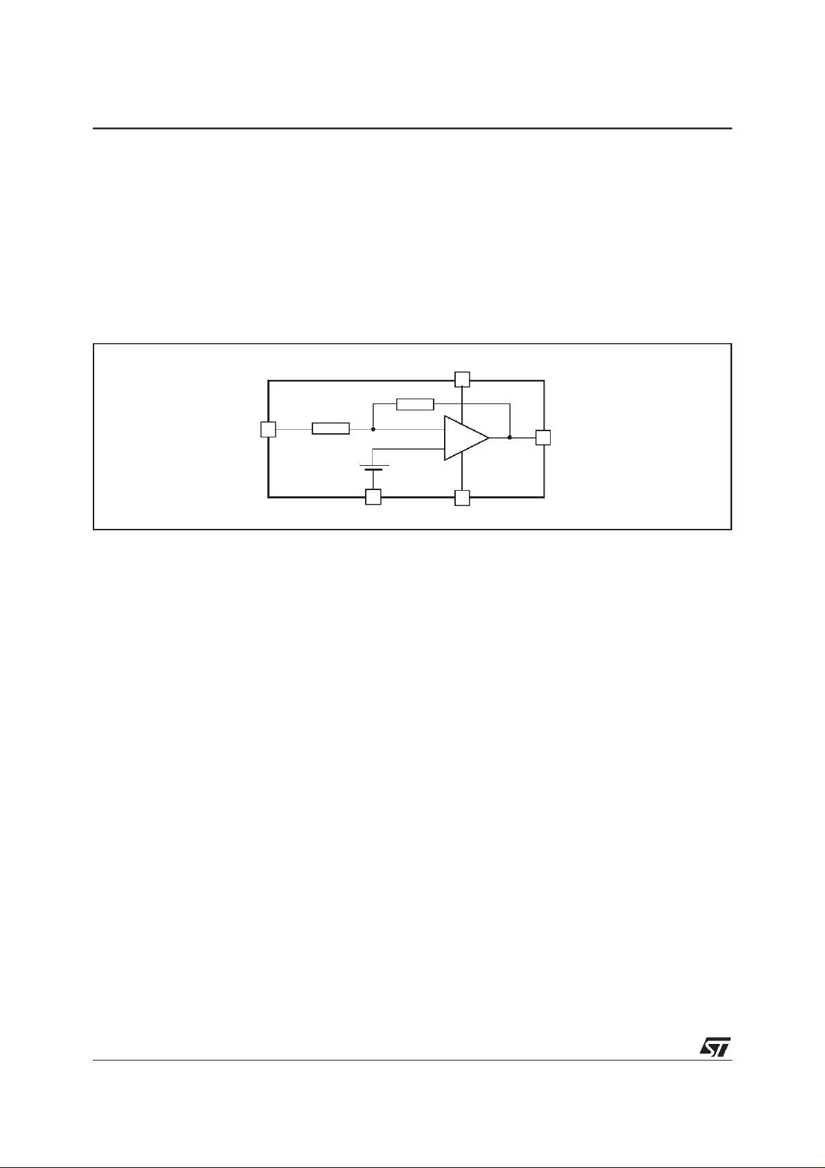
A very simplified schematic of each STV9553 channel is shown in Figure 3.
The feedback network of each channel is integrated with a typical built-in voltage gain of G=20 (40k/2k).
The output voltage V
V
= (G+1) x V
OUT
for G = 20 and V
V
= 117.6 - 20 x V
OUT
REF
REF
is given by the following formula:
OUT
-(GxVIN)
= 5.6V, we have
IN
Figure 3. Simplified schematic of one channel
2k
IN
V
REF
GNDA
40k
V
DD
-
+
GNDP
OUT
8/24
Page 9

STV9553
7 POWER DISSIPATION
The total power dissipation is the sum of the static DC and the dynamic dissipation:
P
TOT=PSTAT+PDYN
The static DC power dissipation is approximately:
P
STAT=VDDxIDD+VCCxICC
The dynamic dissipation is, in the worst case (1 pixel On/ 1 pixel Off pattern):
P
=3VDDxCLxV
DYN
where fis the videofrequency and K the ratio between the active line and the total horizontal lineduration.
Example:
for VDD= 110V, VCC= 12V,
IDD= 15mA, ICC= 40mA,
V
=40VPP, f = 25MHz,
OUT
CL= 8pF and K = 0.72.
We have:
P
= 2.13W and P
STAT
.
OUT(PP)
= 1.90W
DYN
x f x K (see Note 6)
Therefore:
P
=4.03W.
TOT
Note 6: This worst thermal case must only be considered for TJmax calculation. Nevertheless, during the average life
of the circuit, the conditions are closer to the white picture conditions.
9/24
Page 10
STV9553
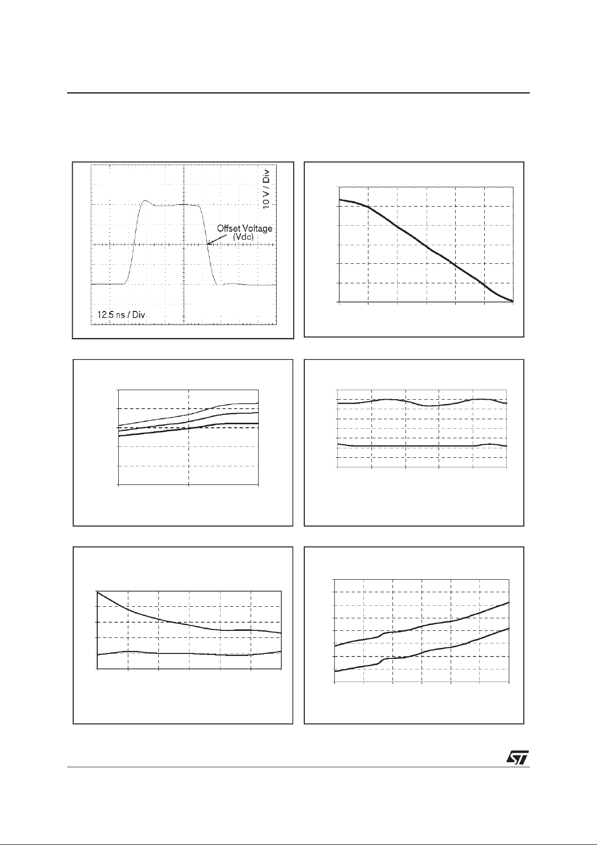
8 TYPICAL PERFORMANCE CHARACTERISTICS
VDD=110V, VCC=12V, CL=8pF, RP=300Ω, ∆V=40VPP, unless otherwise specified - see Figure 1
Figure 4. STV9553 pulse response Figure 5. V
tr=10.8ns
12
overshoot = 5%
120
OUT
versus V
IN
100
80
60
Vout (V)
40
20
tf=12.8ns
12
overshoot = 0%
0
0123456
Vin(V)
Figure 6. Power dissipation versus frequency Figure 7. Speed versus temperature
5.00
4.00
3.00
2.00
Power dissipation (W)
1.00
0.00
10 20 30
Vdd=90V
Frequency (MHz)
(72% active time)
Vdd=100
Vdd=110V
14
13.5
13
12.5
12
11.5
Speed (ns)
11
10.5
10
50 60 70 80 90 100
Tf
Tr
Case Temperature (°C)
Figure 8. Speed versus offset Figure 9. Speed versus load capacitance
18
15
14
13
12
Speed (ns)
11
10
40 45 50 55 60 65 70
Tr
Tf
Offset(Vdc)
10/24
17
16
15
14
Speed (ns)
13
12
11
10
8 101214161820
Tf
Tr
Load capacitance (pF)
Page 11
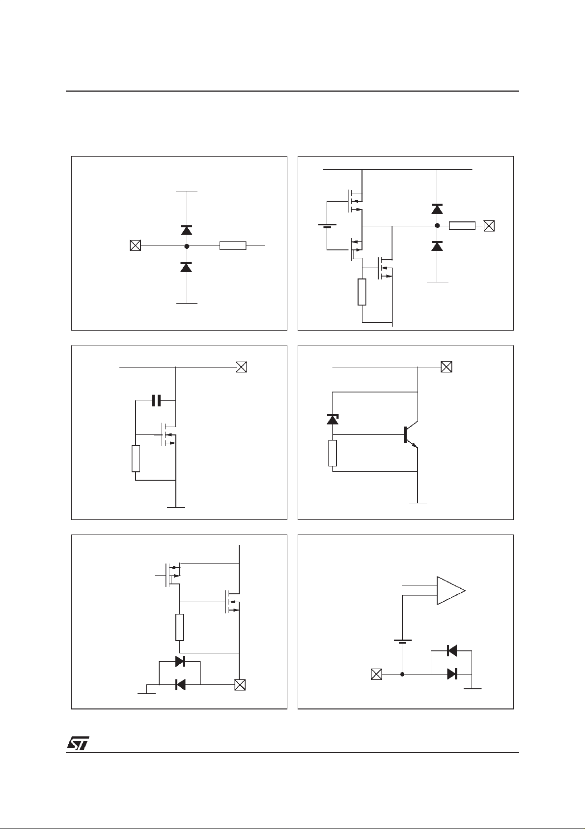
9 INTERNAL SCHEMATICS
Figure 10. RGB inputs Figure 11. RGB outputs
VCC
IN
pins 1, 2, 4
GNDS
Figure 12. VDD Figure 13. VCC
VDD VCC
STV9553
VDD
OUT
pins 9, 10, 11
GNDS
GNDS
Figure 14. GNDP Figure 15. GNDA
GNDA
GNDP
GNDS
GNDS
GNDS
11/24
Page 12

STV9553
10 APPLICATION HINTS
10.1 How to choose the high supply voltage value (VDD) in DC coupling mode
The VDDhigh supply voltage must be chosen carefully. It must be high enough to provide the necessary
video adjustment but set to minimum value to avoid unecessary power dissipation.
Example (see Figure 2):
The following example shows how the optimum VDDvoltage value is determined:
– Cut-off adjustment range (B) : 25V
– Max contrast (D) : 40V
Case 1:
10V Brightness (C) adjusted by the preamplifier :
VDD=A+B+C+D+E
VDD= 15V + 25V + 10V + 40V + 17V = 107V
Case 2:
10V Brightness (C) adjusted by the G1 anode:
VDD=A+B+D+E
VDD= 15V + 25V + 40V + 17V = 97V
10.2 Arcing Protection: schematics
As the amplifier outputs are connected to the CRT cathodes, special attention must be given to protect
them against possible arcing inside the CRT.
Protection must be considered when starting the design of the video CRT board. It should always be
implemented before starting to adjust the dynamic video response of the system.
The arcing network that we recommend (see Figure 16) provides efficient protection without deteriorating
the amplifier video performances.
The total resistance between the amplifier and the CRT cathode (R10+R11) protects the device against
overvoltages. We recommend to use R10+R11 > 300 Ω.
Spark gaps are strongly recommended for arcing protection.
12/24
Page 13
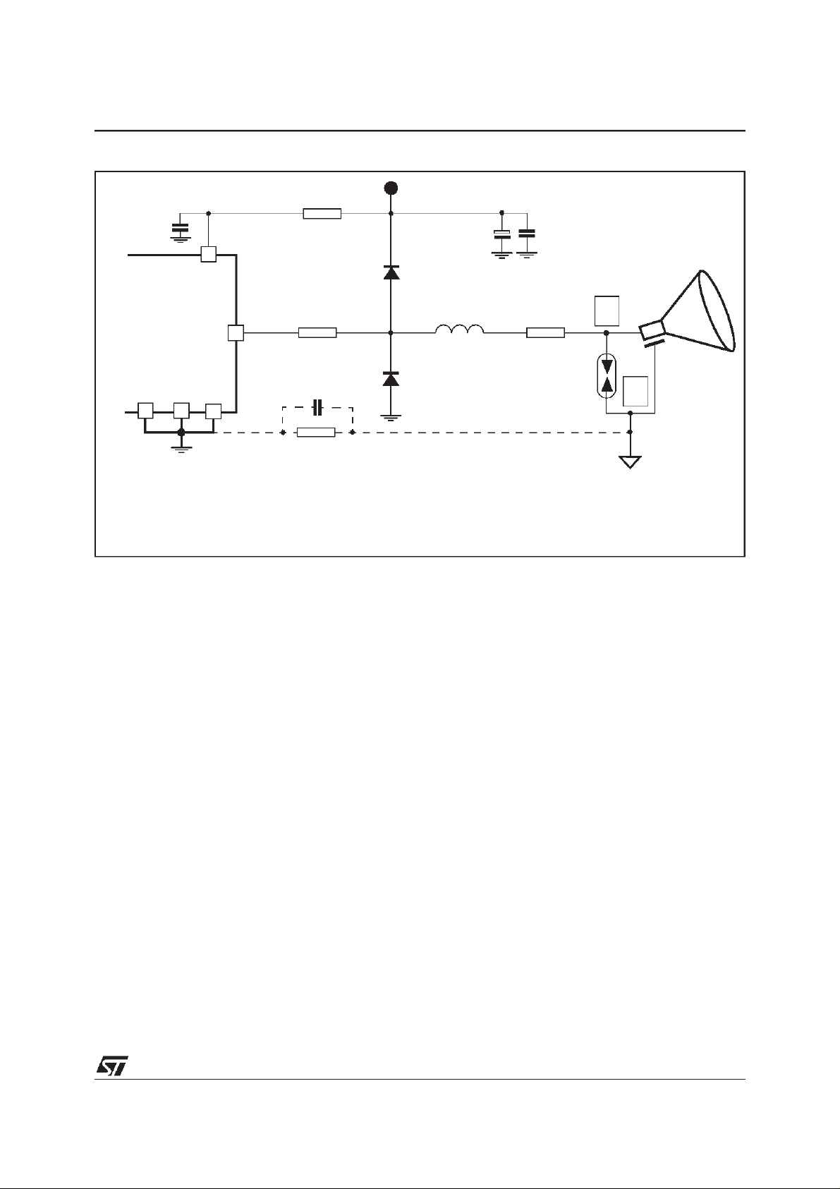
Figure 16. Arcing protection network (one channel)
V
DD
R19(**)
STV9553
C12(*)
100nF/250V
V
DD
OUT
STV9553
GNDS
GNDA
): To be connected as close as possible to the device
(
*
(**): R19 must be mandatorily used
(***): Ground separation network
GNDP
33-40Ω
FDH400
R10
150Ω/0.5W
C29(***)
0.22µF
R29(***)
1-10Ω
D12
4.7µF/150V
D13
FDH400
C24
L1
0.33µH
C18
100nF
R11
150Ω/0.5W
F1
Spark gap
200V
A
10.3 Arcing protection: layout and decoupling
Several layout precautions have to be considered to get the optimum arcing protection:
CRT
B
Sparkgap grounding: when an arc occurs, the energy must flow through the CRT ground without
reaching the amplifier. This is obtained by connecting the sparkgap grounding (point B) to the CRT
ground (socket) via a wide/short trace. Conversely the point B must be connected to the amplifier
ground via a longer/narrower trace.
Grounding separation: In order to set apart theamplifer ground and CRT ground, the R29/C29 network (Figure 16) can be used.
Amplifier grounding: The 3 grounds GNDS, GNDA and GNDP must be connected together as
close as possible to the device.
13/24
Page 14
STV9553
10.4 Video response optimization: schematics in DC-coupling mode
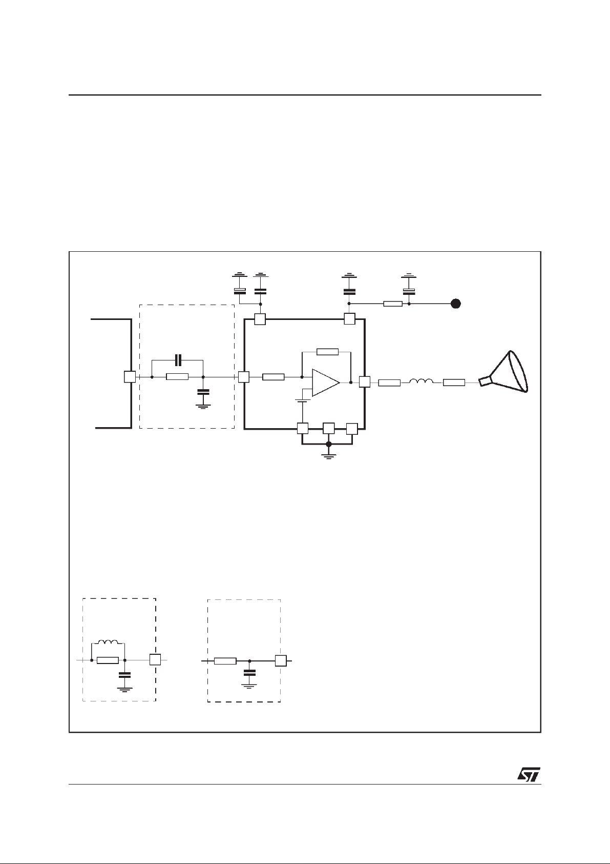
The dynamic video response isoptimized by carefully designing the supply decoupling of the video board
(see Section 10.7), the tracks (see Section 10.7), then by adjusting the input/output component network
(see Section 10.5).
For dynamic measurements such as rise/fall time and bandwidth, a 8pF load is used (total load including
the parasitic capacitance of the PC board and CRT Socket).
When usedinkit with the STV921x preamplifier from ST, the preamplifierbandwidth register (BW, register
13) must be set to minimum (o dec) for an application with tR/tF>5.5ns.
Figure 17. Video response optimization for one channel - DC coupling application
C11
4.7µF
Reference
Input Network #1
C1
1.5nF
OUT
R1(**)
STV921x
Caution: For Application with Tr/Tf>5.5ns, the PreAmplifier bandwidth register (BW, Register 13)
must be set to minimum value (0 dec)
): To be connected as close as possible to the device
(
*
(
): R1 must be not behigher than 100Ω
**
(***): R19 must be mandatorily used
51Ω
C2
10pF
IN
C10(*)
100nF
V
CC
STV9553
V
REF
GNDA
C12(*)
100nF
V
-
+
GNDS
DD
R19(***)
33-40Ω
OUT
R10
150Ω 150Ω0.33µH
GNDP
4.7µF
L1
C24
R11
V
DD
CRT
2 other Input Networks (Network #2 and #3 below) can be used in replacement of the reference Input Network #1.
See Application note AN1510 for complete description.
Input Network#2
L1
0.33µH
R1
82Ω
14/24
IN
C2
10pF
InputNetwork#3
R1
33Ω
C2
15pF
IN
Page 15

STV9553
10.5 Video response optimization: outputs networks
The output network (R10/L1/R11) is used to adjust the amplifier video performances. Once R10 and R11
resistors are set toprotect the application against arcing (R10 + R11>300Ω), it is possible to increase the
bandwidth by increasing L1.
10.6 Video response optimization: inputs networks
The input network also plays an important role in the device dynamic behaviour. We recommend to use
the reference input network #1, whichis described in Figure 17, but 2 other networks (#2 and #3) can be
used to better match the required performances and the video board layout. Refer to the application note
referenced AN1510 for the complete description of these input networks.
10.7 Video response optimization: layout and decoupling
The decoupling of VCCand VDDthrough good quality HF capacitors (respectively C10 and C12) close to
the device is necessary to improve the dynamic performance of the video signal.
Careful attention has to be given to the three output channels of the amplifier.
Capacitor: The parasitic capacitive load on the amplifier outputs must be as small as possible.
Figure 9 from Section 8 clearly shows the deterioration of the tR/tFwhen the capacitive load
increases. Reducing this capacitive load is achieved by moving awaythe output tracks from the other
tracks (especially ground) and by using thin tracks (<0.5mm), see Figure 17.
Cross talk: Output and input tracks must be set apart.The STV9553 pin-out allows the easy separation of input and output tracks on opposite sides of the amplifier (see Figure 21).
Length: Connection between amplifier output and cathode must be as short and direct as possible.
15/24
Page 16
STV9553
10.8 AC - Coupling mode
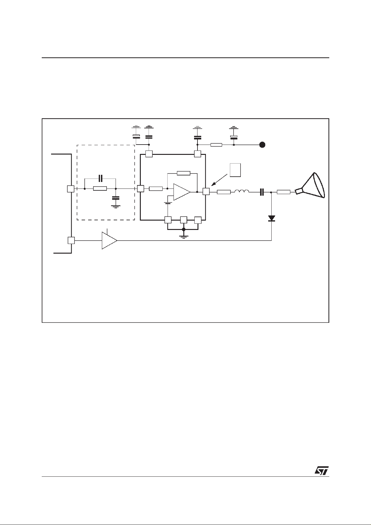
The STV9553 can be used in AC-Coupling mode in kit with the TDA9207/9212 preamplifier from ST. As
for theDC-coupling mode, the STV9553 drives perfectly the video signal in PICTURE BOOST conditions.
A typical schematic is given on the Figure 18 below.
Figure 18. Video response optimization for one channel - AC coupling application
C11
4.7µF
Reference
InputNetwork #1 (****)
C1
1.5nF
OUT
R1(**)
51Ω
TDA9207
Cut-off
Caution: For Application with Tr/Tf>5.5ns, the PreAmplifier bandwidth register (BW, Register 13)
must be set to minimum value (0 dec)
(
): To be connected as close as possible to the device
*
(
): R1 must be not be higher than 100Ω
**
(***): R19 must be mandatorily used
(****): Input Networks #2 and #3 can be used as well
V
DC Restore
circuitry
C2
10pF
restore
C10(*)
100nF
V
STV9553
IN
V
REF
GNDA
CC
C12(*)
100nF
V
-
+
GNDS
DD
R19(***)
33-40Ω
OUT
R10 L1 R11
150Ω 150Ω0.33µH
GNDP
C
C24
4.7µF
C1
1µF
V
DD
CRT
The advantage of such an architecture is to use smaller VDDand therefore to have smaller power
consumption. This is due to the fact that the STV9553 provides only the video signal and not the cut-off
adjustment. The disadvantage is to have an application with more components (DC restore circuitry).
Note that it is mandatory to keep the output video signal (point C) inside the linear area of the amplifier
(from 17V to VDD- 15V).
16/24
Page 17
10.9 Stand-by mode, spot suppression
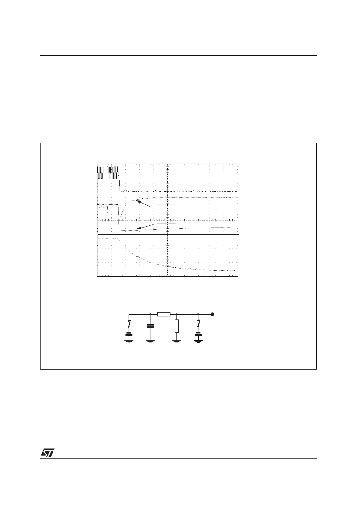
The usual way to set a monitor in stand-by mode is to switch-off the Vcc (12V).
STV9553
The STV9553 has an extremely low power consumption (I
=60µA when VCC<1.5V) instand-by mode
DDS
and the outputs are set to low level (white picture).
To avoid the display of a spot effect during the switch-off phase, it is necessary to adjust the G1 circuitry
(Resistors Rx and Cx, see Figure 19) to pull the G1 voltage to low value during a sufficient time duration.
Figure 19. Stand-by mode, spot effect
+80V
Cathode
0V
-30V
G1
-120V
EHT
(27kV)
Case #1: Low Rx.Cx
A spot might appear during
the switch-off phase
Case #2: High Rx.Cx
No spot effect
Typical G1 generator circuitry
Cx
-120V -30V
Rx
G1R1
17/24
Page 18

STV9553
10.10 Conclusion
Video response is always a compromise between several parameters. For example, the rise/fall time
improvement leads to the overshoot deterioration.
The recommended way to optimize the video response is:
1 Toset R10+R11 for arcing protection (min. 300 Ω)
2. To adjust R20 and R10+R11.
Increasing their value increases the
tR/tFvalues and decrease the overshoot
3. To adjust L1
Increasing L1 speeds up the device but increases the overshoot.
4. To adjust the input network for the final dynamic tunning (e.g.: critical damping)
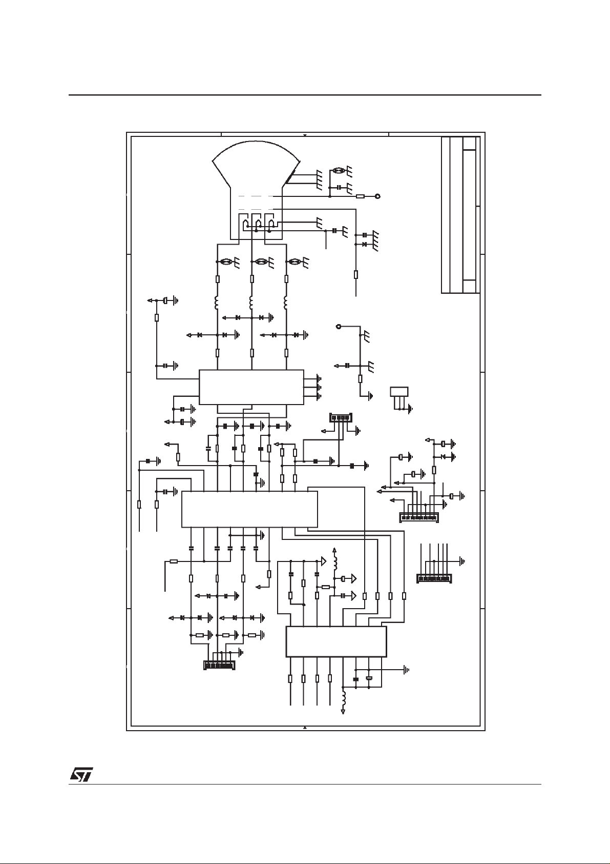
We recommend our customers to use the schematic shown on Figure 23 as a starting point for the video
board and then to apply the optimization they need.
18/24
Page 19
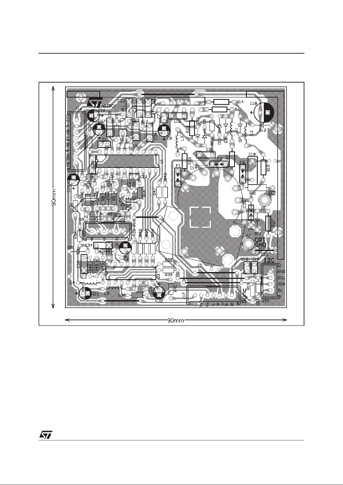
Figure 20.STV9553/9555/9556 + TDA9210/STV9211 + STV9936 S/P
DC-coupling demonstration board: Silk Screen and Trace
STV9553
19/24
Page 20
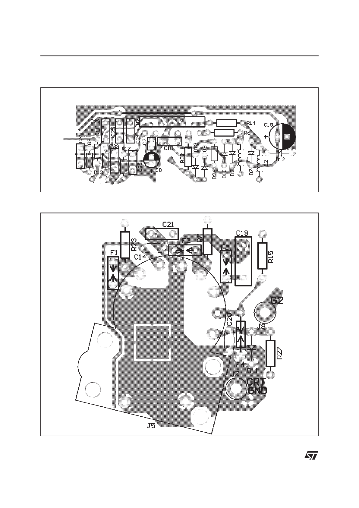
STV9553
Figure 21. Outputs trace (from figure 19)
Figure 22. CRT socket trace (from figure 19)
20/24
Page 21
STV9553
Figure 23. STV9553/55/56 + STV9936 + TDA9210/STV9211 DC-coupling demo - board schematic
Rev.
C
F3
C13
C3410nF
R445.6kΩ
Vco
R35100Ω
5V
100pF
14
VCO
3
4.7nF/2kV
C14
Heater
GND
110V
J10
123
TDA9210
3.3V
L4 1µH
R43
1MΩ
AVdd
13
AVDD
4
R41100Ω
C19
100nF
J7
SDA
C2
L5 1µH
C37
12
5
1.5Ω
C21
FBLK
DVDD
3.3V
R31
R27
G1
10nF/250V
optional
R280Ω
I2C
4
C12
100pF
100µF/25V
100nF
11
BOUT
DVSS
6
C28100nF
30Ω/0.5W
C20
D11
150Ω/0.25W
R36330Ω
10
7
C32
4.7nF/1kV
1N4004
8V
12V
R32330Ω
9
GOUT
TEST
OVDD ROUT
8
100µF/25V
J8
G2
HS1
123
5V
110V
R33330Ω
STV9936S/P
C16
47µF/25V
1234567
J16
R34330Ω
STMicroelectronics
MonitorBusinessUnit- Videoapplication
CMG- Imagingand DisplayDivision(IDD)
12, rueJulesHorowitz-B.P. 217
RadAB20
3.3V
C15
47µF/25V
BLK
G1
HEATERVSHS
7654321
J17
38019Grenoblecedex- FRANCE
R3751Ω
8
C27
ZD1
ABL
Power
47µF/25V
3V0
C27
HFLY
EVALCRT52/STV955xdemoboard(AB25)
Version1.4
47µF/25V
Sync
WednesdayOctober3, 2001
12
GND
GND
1
G2
7
5
G1
CRT smallneck
R
B
G
RK
R7
110V
100nF
47µF/25V
20
1
100nF
C3
R215Ω
1N4148
Blue
D2
7
3
IN1 BLK
5V
D3
R3
L1
FDH400
R6
Vdd
Vcc
1.5nF
R9 51Ω
C31
19
ABL HS/CLP
2
100nF
C4
D4
1N4148D51N4148
1N4148
75Ω
12345
J1
11
1
18
3
Green
110V
C18
4.7µF/160V
R2939Ω
C10
10nF/250V
C7
12V
C8
8V
C1
100pF
R112.7Ω
C26
100pF
R1100Ω
R25100Ω
BLK
ABL
U1
R4
2.7Ω
5V
D1
HS
F2
200V
110Ω/0.25W
0.33µH
110V
D10
FDH400
110Ω/0.25W
In1 Out1
C23
10pF
1.5nF
C33
171615
GNDL VCCP
IN2 OUT1
4
C9 100nF
R8 15Ω
5V
D6
R5
75Ω
6
D7
FDH400
U2
R13 51Ω
IN3 OUT2
5
C6 100nF
R1215Ω
1N4148
Red
video
GK
R15
L2
0.33µH
R14
10
STV9553
In2 Out2
2
C24
10pF
C5 100nF
6
C22100nF
D8
R10
75Ω
F4
200V
110Ω/0.25W
D12
110V
110Ω/0.25W
1.5nF
C36
GNDP
GNDA
1N4148
FDH400
D9
C25
5V
R17 51Ω
141213
VCCA OUT3
7
R162.7Ω
FDH400
R192.7kΩ
BK
R23
L3
R22
9
In3 Out3
4
10pF
R40100Ω
OSD1 SDA
8
R465.6kΩ C35 10nF
U3
1
R38100Ω
SDA
H2
H1
F1
200V
110Ω/0.25W
0.33µH
D13
FDH400
110Ω/0.25W
GNDP
GNDS
GNDA
SCL
R212.7kΩ
R47100Ω
11
OSD2 SCL
9
10
R4515kΩ
Rp
16
15
RP
AVSS
SDA
SCLVSHFLY
2
R39100Ω
SCLVSHFLY
9
10
8
6
5
OSD3 FBLK
21/24
Page 22
STV9553
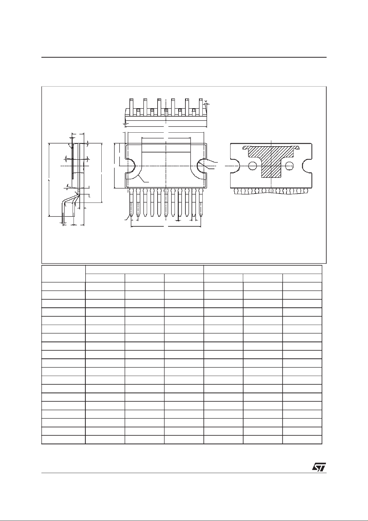
11 PACKAGE MECHANICAL DATA
11 PIN - CLIPWATT
C
V2
V1
V
R3
R3
E
M1
Dimensions
V1
L3
L2
LEAD#1
S
G
A
V1
V1
L1
D
R3
B
M
Millimeters Inches
Min. Typ. Max. Min. Typ. Max.
H3
H2
H1
R2
R
R1
F
F1
G1
Shaded area ewposedfrom plasticbody
Typical30 µm
A 2.95 3 3.05 0.116 0.118 0.12
B 0.95 1 1.05 0.037 0.039 0.041
C - 0.15 - - 0.006 D 1.3 1.5 1.7 0.051 0.059 0.061
E 0.49 0.515 0.55 0.0.019 0.02 0.021
F 0.78 0.8 0.86 0.03 0.031 0.034
F1 - 0.05 0.1 - 0.002 0.004 (6)
G 1.6 1.7 1.8 0.063 0.067 0.071
G1 16.9 17 17.1 0.665 0.669 0.673
H1 - 12 - - 0.472 H2 18.55 18.6 18.65 0.73 0.732 0.734
H3 19.9 20 20.1 0.783 0.787 0.791 (5)
L 17.7 17.9 18.1 0.696 0.704 0.712
L1 14.35 14.55 14.65 0.564 0.572 0.576
L2 10.9 11 11.1 0.429 0.433 0.437(5)
L3 5.4 5.5 5.6 0.212 0.216 0.22
M 2.34 2.54 2.74 0.092 0.1 0.107
M1 2.34 2.54 2.74 0.092 0.1 0.107
R 1.45 - - 0.057 - -
22/24
Page 23
STV9553
Dimensions
R1 3.2 3.3 3.4 0.126 0.13 0.134
R2 - 0.3 - - 0.012 R3 - 0.5 - - 0.019 -
S 0.65 0.7 0.75 0.025 0.027 0.029
V 10deg. 10deg.
V1 5deg. 5deg.
V2 75deg. 75deg.
Note 5: “H3 and L2” do not include mold flash or protrusions
Mold flash or protrusions shall not exceed 0.15mm per side.
Note 6: No intrusions allowed inwards the leads
Min. Typ. Max. Min. Typ. Max.
Millimeters Inches
Critical dimensions:
Lead split (M1)
Total length (L)
23/24
Page 24

STV9553
Information furnished is believed to be accurate and reliable. However, STMicroelectronics assumes no responsibility for
the consequences ofuse of such information nor for any infringement of patents or other rights of third parties which may
result from its use. No license is granted by implication or otherwise under any patent or patent rights of
STMicroelectronics. Specifications mentioned in this publication are subject to change without notice. This publication
supersedes and replaces all information previously supplied. STMicroelectronics products are not authorized for use as
critical components in life support devices or systems without express written approval of STMicroelectronics.
The ST logo is a trademark of STMicroelectronics.
2002 STMicroelectronics - All Rights Reserved
Purchase of I2C Components of STMicroelectronics, conveys a license under the Philips I2C Patent.
Rights to use these components in a I2C system, is granted provided that the system conforms to the I2C Standard
Specifications as defined by Philips.
Australia - Brazil - China - Finland - France - Germany -Italy - Japan - Korea - Malaysia - Malta - Mexico - Morocco -The
Netherlands - Singapore - Spain - Sweden - Switzerland - Taiwan - Thailand - United Kingdom - U.S.A.
24/24
STMicroelectronics GROUP OF COMPANIES
http://www.st.com
4
Page 25

WWW.ALLDATASHEET.COM
Copyright © Each Manufacturing Company.
All Datasheets cannot be modified without permission.
This datasheet has been download from :
www.AllDataSheet.com
100% Free DataSheet Search Site.
Free Download.
No Register.
Fast Search System.
www.AllDataSheet.com
 Loading...