

Page 1
®
Mono and Colour QSIF Digital Video CMOS Image Sensors
cd5301-6301f: Rev 3.0, 25 September 2000
1/50
VV5301 & VV6301
Commercial in confidence
The VV5301 and VV6301 are highly integrated digital
output imaging devices based on STMicroelectronics’s
unique CMOS sensor technology. Both of these sensors
require minimal support circuitry and provide an ideal low
cost imaging solution.
VV5301 (monochrome) and VV6301 (colourised) produce
digital video output. The video streams from both devices
contain embedded control data that can be used to enable
frame grabbing applications.
The pixel array of the VV6301 has colour filters forming a
Bayer colour pattern. This sensor requires software to
perform colour processing to allow an image to be
displayed on a PC.
The sensor can perform automatic black calibration to
remove voltage offsets in the video signal path that lead to
offsets in the output image. These offsets are removed
using 2 Digital to Analogue Convertors (DACs). The
automatic black calibration algorithmmonitorsthe average
level of the sensor black pixels and adjusts the input level
to the 2 DACs to remove the offset.
A 2 wire serial interface allows the sensor to be
reconfigured if required.
Functional block diagram
SAMPLE & HOLD
HORIZONTAL SHIFT REGISTER
PHOTO DIODE ARRAY
ANALOG
VOLTAGE
REFS.
DIGITAL
CONTROL
LOGIC
SDA
SCL
D[7:0]
VERTICAL
SHIFT
REGISTER
CLKI
CLKO
CLOCK
CIRCUIT
IMAGE
FORMAT
A/D CONVERTOR
SIN
FST
QCK
Key Features
• QSIF resolution sensor
• Automatic exposure/gain control
• Multiple digital output formats available
• I2C interface for sensor control
• Integrated 8bit ADC
• On board voltage regulator
• Automatic Black Calibration
• Variable frame rate
• Reduced flicker operating modes
Application Areas
• Toys
• Automotive systems
• Intelligent Imaging sensors
Specifications
Maximum pixel
resolution
164 x 124
Effective image
size after colour
processing
160 x 120
Pixel size 12.0µm x 12.0µm
Array size 1.92mm x 1.44mm
Exposure control Automatic ( to +44dB)
Analogue gain +18dB
Signal/Noise ratio 36dB
Supply voltage 5V DC +/− 5%
Supply current
VV5301-VV6301
2.9mA (standby)
14.6mA (active)
Operating
temperature
(ambient)
0
o
C - 40oC
(for extended temperature information please contact STMicroelectronics)
Package type 48BGA
Page 2

VV5301 & VV6301
cd5301_6301f-3-0.fm
Commercial in confidence
2/50
Table of Contents
2. Introduction ...................................................................................................................... 5
2.1 Overview...........................................................................................................................................5
2.2 Exposure, Clock Division and Gain Control......................................................................................5
2.3 Digital Interface.................................................................................................................................5
3. Operating Modes.............................................................................................................. 7
3.1 Video Timing.....................................................................................................................................7
3.2 Pixel Array.........................................................................................................................................7
3.3 System Clock Generation...............................................................................................................10
3.4 Calculating Sensor Framerate........................................................................................................10
4. Auto Black Calibration................................................................................................... 12
5. Exposure Control........................................................................................................... 13
4. Auto Black Calibration................................................................................................... 12
5. Exposure Control........................................................................................................... 13
5.1 Calculating Exposure Period...........................................................................................................13
5.2 Automatic Exposure Control...........................................................................................................13
5.3 Updating Exposure, Gain and Clock Division Settings...................................................................13
5.4 Clock Control ..................................................................................................................................13
5.5 Gain Setting....................................................................................................................................14
6. Timed Serial Interface Parameters ............................................................................... 15
6.1 Listing and Categorizing the Parameters........................................................................................15
6.2 Timed Parameter Update Points.....................................................................................................15
7. Digital Video Interface Format ...................................................................................... 16
7.1 Embedded control data...................................................................................................................16
7.2 8-Wire Parallel Mode ......................................................................................................................18
7.3 4-Wire Parallel Mode ......................................................................................................................18
7.4 Video Frame Composition ..............................................................................................................19
7.5 Qualifying the Output Data..............................................................................................................23
8. Serial Control Bus.......................................................................................................... 27
8.1 General Description........................................................................................................................27
8.2 Serial Communication Protocol.......................................................................................................27
8.3 Data Format....................................................................................................................................27
8.4 Message Interpretation...................................................................................................................28
8.5 The Programmers Model ................................................................................................................29
8.6 Types of messages.........................................................................................................................39
8.7 Serial Interface Timing....................................................................................................................41
9. Detailed AC/DC Specification........................................................................................ 43
Page 3

CMOS Sensor; Customer Datasheet, Rev 3.0, 25 September 2000 VV5301 & VV6301
3/50
cd5301_6301f-3-0.fm
Commercial in confidence
9.1 VV5301/VV6301 AC/DC Specification............................................................................................43
9.2 VV5301/VV6301 Power Consumption............................................................................................43
9.3 Digital Input Pad Pull-up and Pull-down Resistors..........................................................................43
10. Pinout and Pin Descriptions ......................................................................................... 44
11. VV5301/VV6301 Recommended Reference Design..................................................... 46
12. Package Details (48 pin BGA (VV5301/VV6301) .......................................................... 47
13. Evaluation kits (EVK’s) .................................................................................................. 48
14. Ordering Details .............................................................................................................49
Page 4
VV5301 & VV6301
cd5301_6301f-3-0.fm
Commercial in confidence
4/50
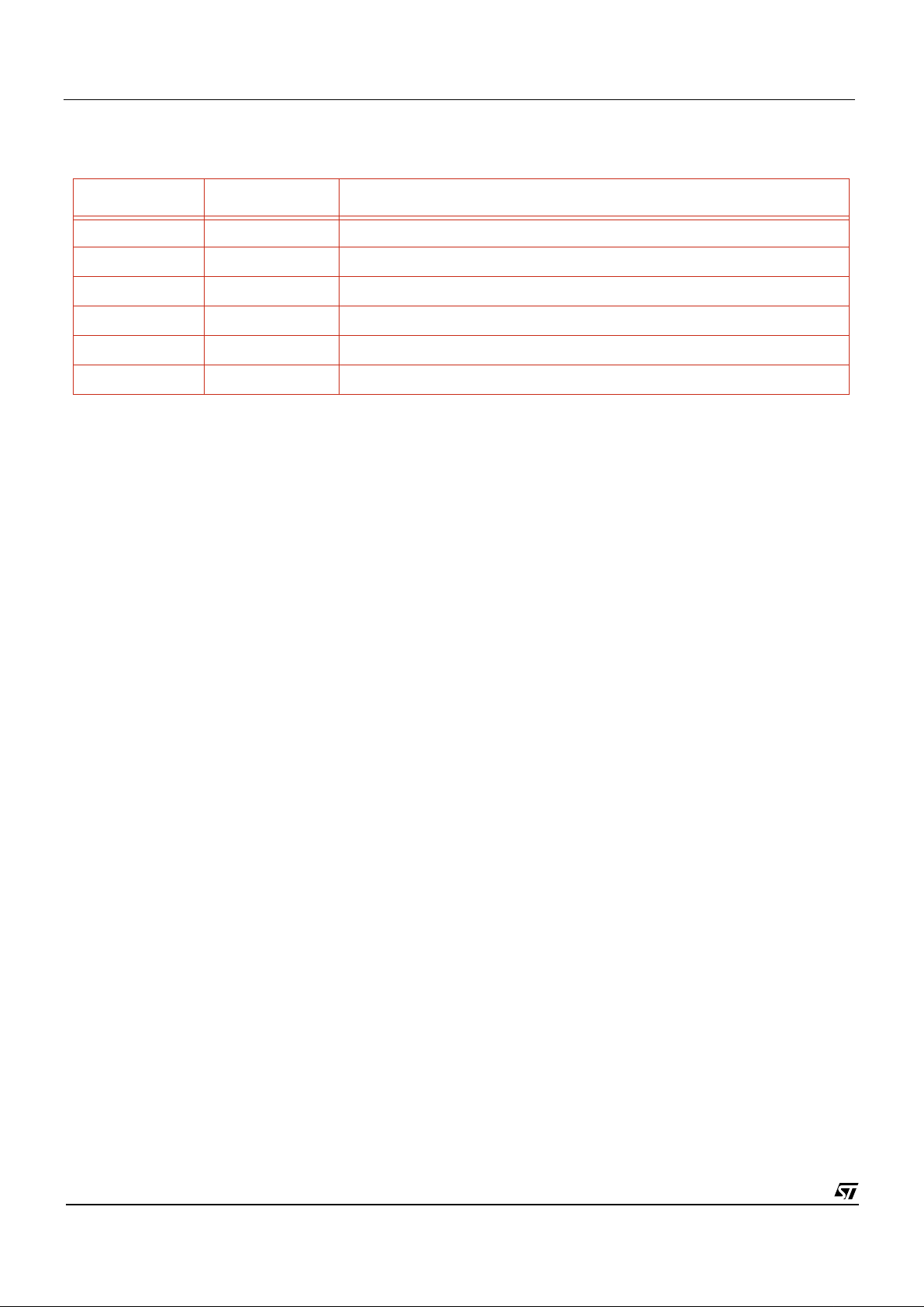
1. Document Revision History
Revision Date Comments
1.0 03/07/2000 Preliminary release
1.1 05/07/2000 Full datasheet release, correcting formatting of document
Table 1 : Document Revison History
Page 5
CMOS Sensor; Customer Datasheet, Rev 3.0, 25 September 2000 VV5301 & VV6301
5/50
cd5301_6301f-3-0.fm
Commercial in confidence
2. Introduction
2.1 Overview
VV5301/VV6301 is a QSIF format CMOS image sensor. The VV5301 sensor is a monochrome device and the VV6301 is the
colourised variant.
Important: The sensors’ output video data stream only contains raw data. A microprocessor and supporting software are
required to generate a video waveform that can be displayed on a VDU
VV5301/VV6301 have an on-board 8bit ADC, this limits the number of components required to form a complete digital imaging
system.
The VV5301/VV6301 sensor will output an image size of 164 x 124. This is an oversized QSIF image. The extra pixels that the
form the 2 pixel deep border that surrounds the true QSIF image are made available to the external colour processing algorithm.
2.2 Exposure, Clock Division and Gain Control
VV5301/VV6301 have an internal automatic exposure/gain control algorithm. This algorithm can be disabled allowing the user to
externally control the exposure. The externally calculated exposure, clock division and gain control settings would then be written
to the sensor via the I2C interface.
2.3 Digital Interface
VV5301/VV6301 have a flexible digital interface, the main components of which are listed below:
1. A tri-stateable 8-wire data bus (D[7:0]) for sending both video data and embedded timing references.
2. 4-wire and 8-wire data bus alternatives available.
3. A data qualification clock, QCK, which can be programmablevia the serial interface to behave in a number of different ways
(Tri-stateable).
4. A line start signal, LST (Tri-stateable).
5. A frame start signal, FST (Tri-stateable).
6. OEB tri-states all 5 data bus lines, D[4:0], the qualification clock, QCK and FST.
7. The ability to synchronise the operation of multiple cameras (sensor produces a synchronisation out pulse, SNO).
8. A 2-wire serial interface (SDA,SCL) for controlling and setting up the device.
2.3.1 Digital Data Bus
Along with the pixel data, codes representing the start and end of fields and the start and end of lines are embedded within the
video data stream to allow a co-processor to synchronise with video data the camera module is generating Section 7.defines the
format for the output video data stream.
2.3.2 Frame Grabber Control Signals
To complement the embedded control sequences the data qualification clock (QCK) and the field start signal (FST) signals can
be independently set-up as follows:
1. Disabled
2. Free-running.
3. Qualify only the control sequences and the pixel data.
4. Qualify the pixel data only
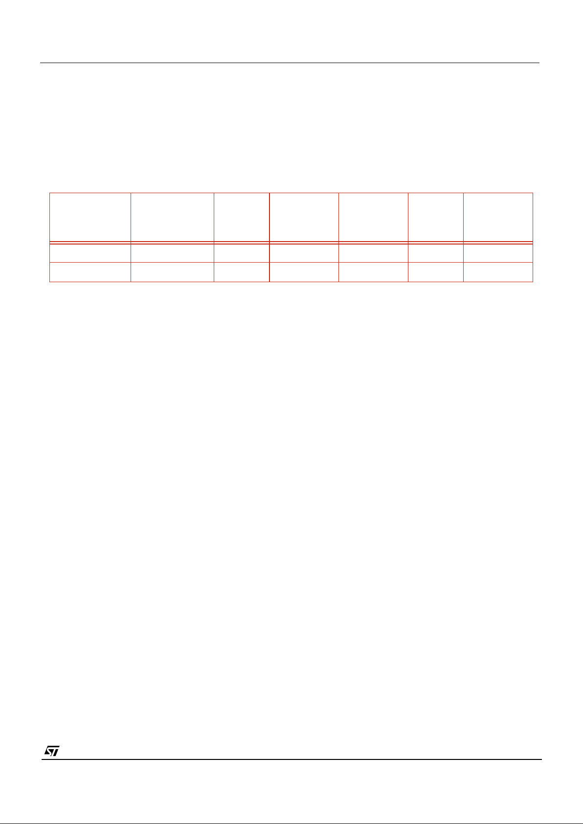
Mode
Input Clock
(MHz)
Note
System
Clock
Divisor
Image Size
Line Time
(µs)
Lines
per
Frame
FrameRate
(fps)
QSIF - 25 fps
14.318 1 164 x 124 271.502 147 25.06
QSIF - 30 fps
17.73 1 164 x 124 227.36 147 29.92
Page 6

VV5301 & VV6301 Introduction
cd5301_6301f-3-0.fm
Commercial in confidence
6/50
2.3.3 2-wire Serial Interface
The 2-wire serial interface provides complete control over sensor setup and operation. Two serial interface broadcast addresses
are supported. One allows all sensors to be written to in parallel while the other allows all sensors and co-processors to be written
to in parallel.
Section 8. defines the serial interface communications protocol and the register map of all the locations which can be accessed
via the serial interface.
2.4 Other Features
2.4.1 Tristating Digital Outputs
The QCK, FST and Databus[7:0] pins can be tristated. The QCK pin can be independently tristated by driving the QCKTRI pin
low. The QCK, FST and upper nibble of the Databus can also be tristated via a serial register control bit, see register[116] for
more details. The lower nibble of the Databus can also be independently tristated using a different control bit in register[116].
2.4.2 Synchronising Video Timing
The video timing logic in VV5301/VV6301 can be synchronised, i.e. reset to the beginning of a timing field, by an external pin,
SIN. This pin is normally low. To enable the synchronising feature the user must drive the pin high for a number of clock periods,
c.10 CLKI periods, then drive it low again. This synchronisation should only be done every other field as the sensor has a 2 field
repeat cycle requirement for the video timing. If the SIN pin was asserted every field the exposure controller and application of
new external exposure and gain settings would not operate correctly.
2.4.3 Pixel Hold Feature
The HPIX signal can be used to freeze the internal ADC, forcing the sensor to stop converting new pixel values. If the HPIX is
driven high then the ADC will maintain the currently converted pixel value. This feature is intended to function as an external pixel
defect correction system, albeit a ver basic example.
Page 7
CMOS Sensor; Customer Datasheet, Rev 3.0, 25 September 2000 VV5301 & VV6301
7/50
cd5301_6301f-3-0.fm
Commercial in confidence
3. Operating Modes
3.1 Video Timing
The video format mode on power-up is QSIF 30fps by default, although a 25fps mode can also be selected, see serial
register[17], bit 6. The number of active video lines in each mode is the same (124) for both the QSIF modes. The slower frame
rate (25 fps) is implemented by simply extending the line period from 203 pixel periods to 301 pixel periods.
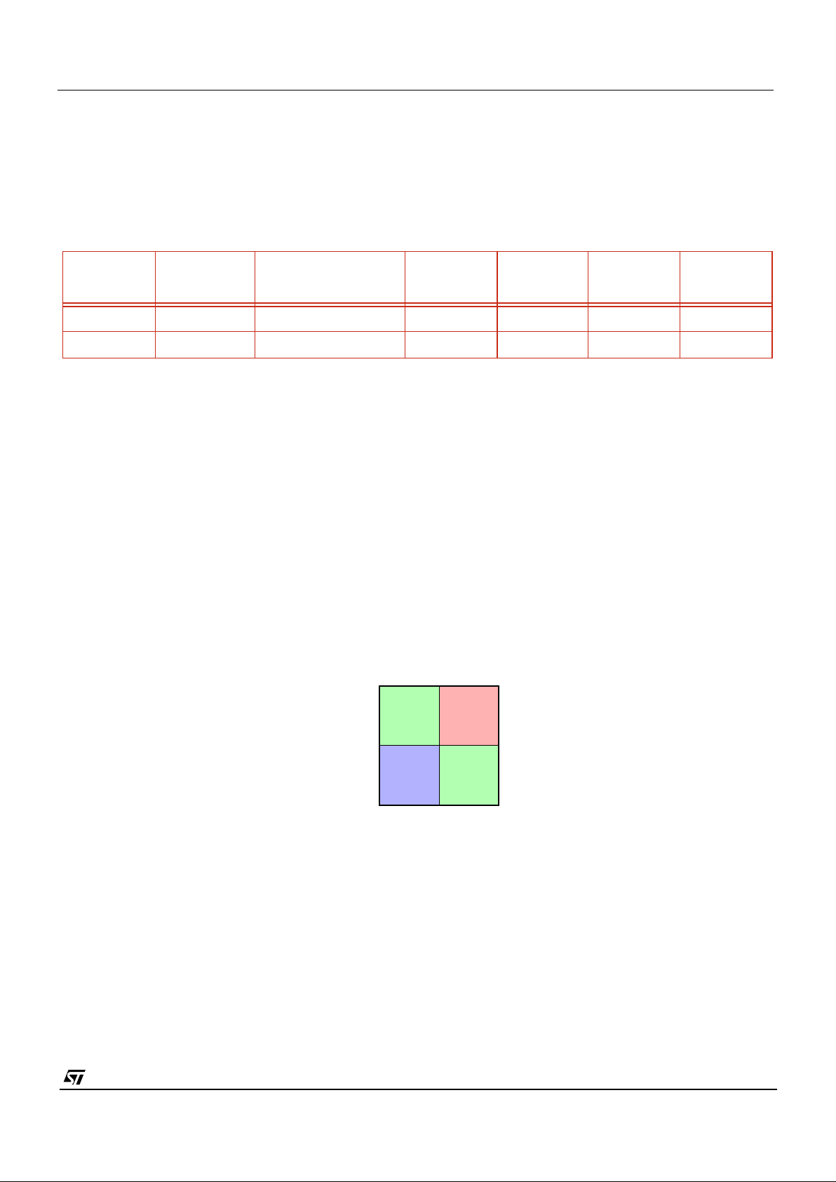
Table 2 details the setup for each of the video timing modes.
3.2 Pixel Array
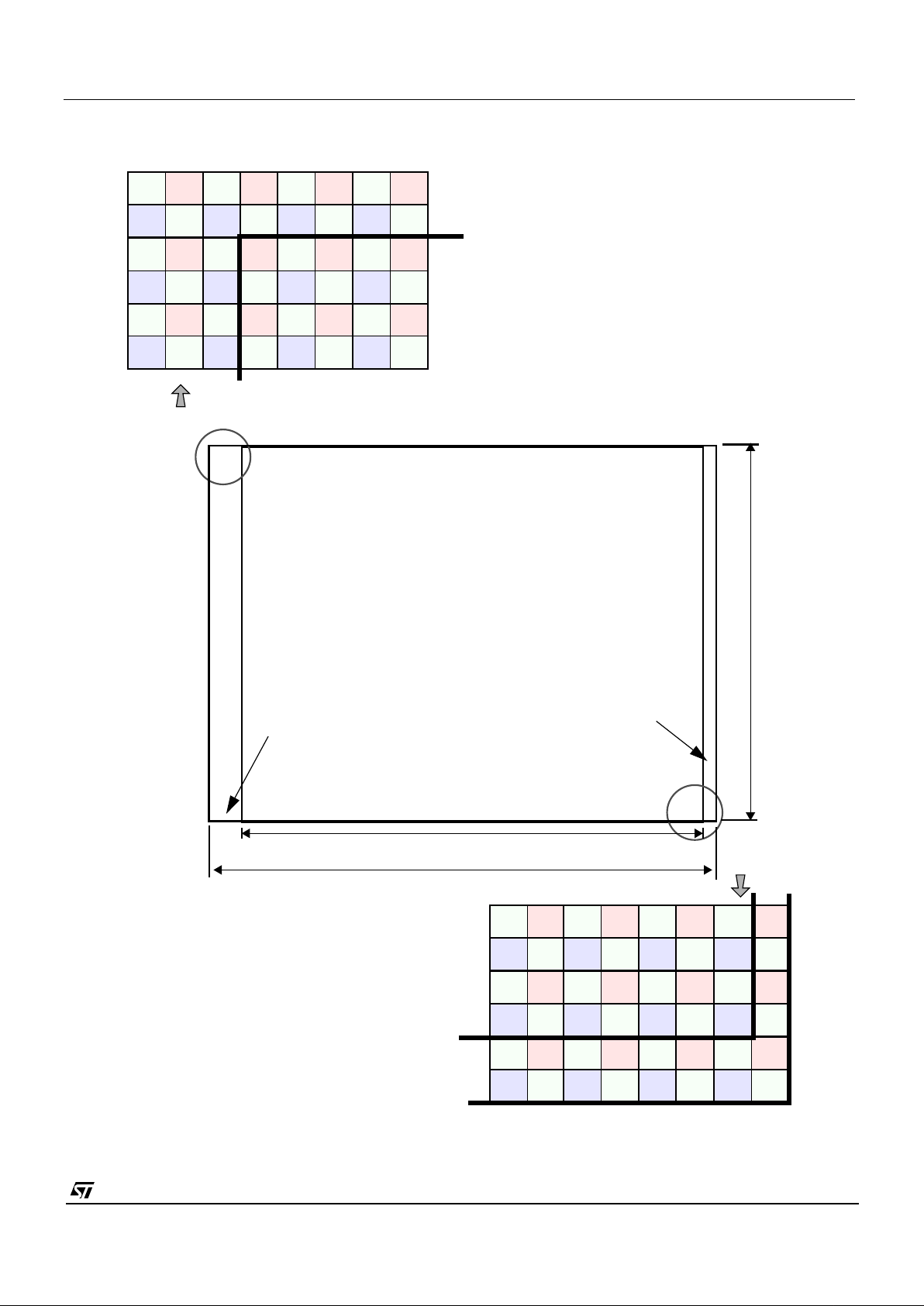
The physical pixel array is 168 x 124 pixels. The pixel size is 12.0 µm by 12.0 µm. The output video image size is 164 x 124
pixels. The border pixels from the array are used as a shield from edge effects.
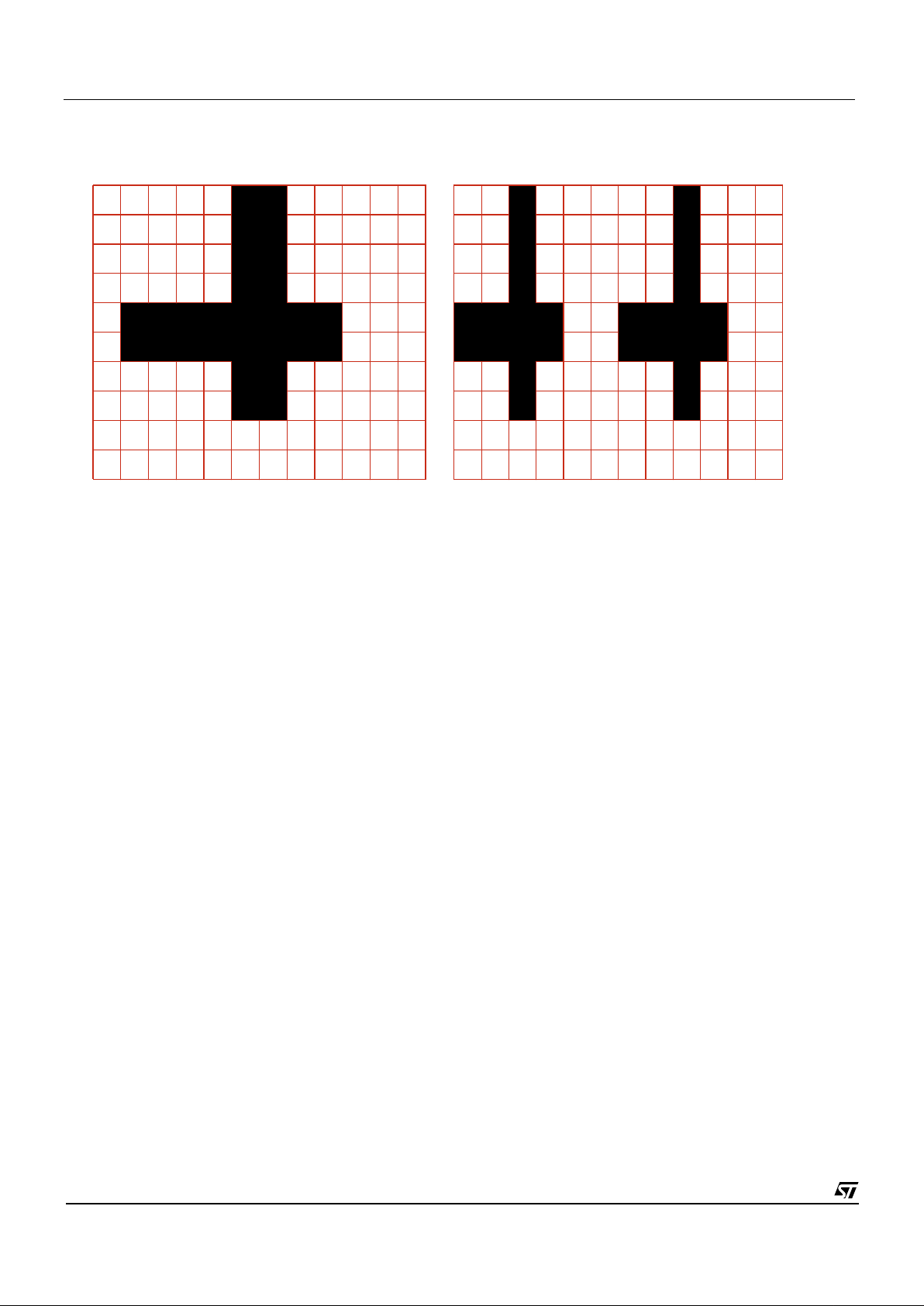
Figure 3 shows how the 164 x 124 is aligned within the bigger 168 x 124 pixel array. Image read-out is flexible. By default the
sensor read out is configured to be horizontally ‘non-shuffled’ non-interlaced raster scan. The horizontally ‘shuffled’ raster scan
order differs from a conventional raster in that the pixels of individual rows are re-ordered, with the even pixels within a row readout first, followed by the odd pixels. This ‘shuffled’ read-out within a line, groups pixels of the same colour (according to the Bayer
pattern - Figure 1) together, reducing cross talk between the colour channels. The horizontal shuffle option would normally only
be selected with the colour sensor variant, VV6301.
Video
Mode
Clock
(MHz)
System Clock Divisor Video Data Line Length Field
Length
Output
Mode
QSIF (30fps) 14.318 1 164 x 124 203 147 4-wire
QSIF (25fps) 17.73 1 164 x 124 301 147 4-wire
Table 2 : Video Timing Modes
Figure 1 : Bayer Colourisation Pattern (VV6301 only)
Green 1
Blue Green 2
Red
Odd Rows
(0,2,4,6,...)
Even Rows
(1,3,5,7,...)
Odd
Columns
(0,2,4,6,...)
Even
Columns
(1,3,5,7,...)
Page 8
VV5301 & VV6301 Operating Modes
cd5301_6301f-3-0.fm
Commercial in confidence
8/50
RRRRRRGGGGGGGRGRGRGRGRGR
Where G - Green and R - Red
Figure 2 : Horizontal Shuffle Enabled
Page 9
CMOS Sensor; Customer Datasheet, Rev 3.0, 25 September 2000 VV5301 & VV6301
9/50
cd5301_6301f-3-0.fm
Commercial in confidence
Blue Green
Green Red
Blue Green
Green Red
164 Pixels
124 Pixels
4321
2
4
3
1
65
1,2,3,4,5,6,... ..., 164,165,166,167,168
1,2,3,4,5,6,8,...
.120.,121,122,123,124
Blue Green
Green Red
6
5
87
164163162161 166165
168167
168Pixels
Blue Green
Green Red
Blue Green
Green Red
Blue Green
Green Red
Blue Green
Green Red
Blue Green
Green Red
Blue Green
Green Red
Blue Green
Green Red
Blue Green
Green Red
Blue Green
Green Red
Blue Green
Green Red
Blue Green
Green Red
Blue Green
Green Red
Blue Green
Green Red
Blue Green
Green Red
Blue Green
Green Red
Blue Green
Green Red
Blue Green
Green Red
Blue Green
Green Red
Blue Green
Green Red
Blue Green
Green Red
Blue Green
Green Red
The colour dyes included in this
diagram are only applicable to
VV6301. The monochrome device
VV5301 has exactly the same
readout structure and array size as
VV6301 - but no colourised pixels
120
122
121
119
124
123
Figure 3 : Image Readout Order
Please note the column read out order. If the
readout is unshuffled then the readout order is
even,odd,even etc. If the readout is shuffled, to
avoid colour channel crosstalk, then all the even
columns are readout first followed by the odd
columns.
3 pixel band
1 pixel band
Page 10
VV5301 & VV6301 Operating Modes
cd5301_6301f-3-0.fm
Commercial in confidence
10/50
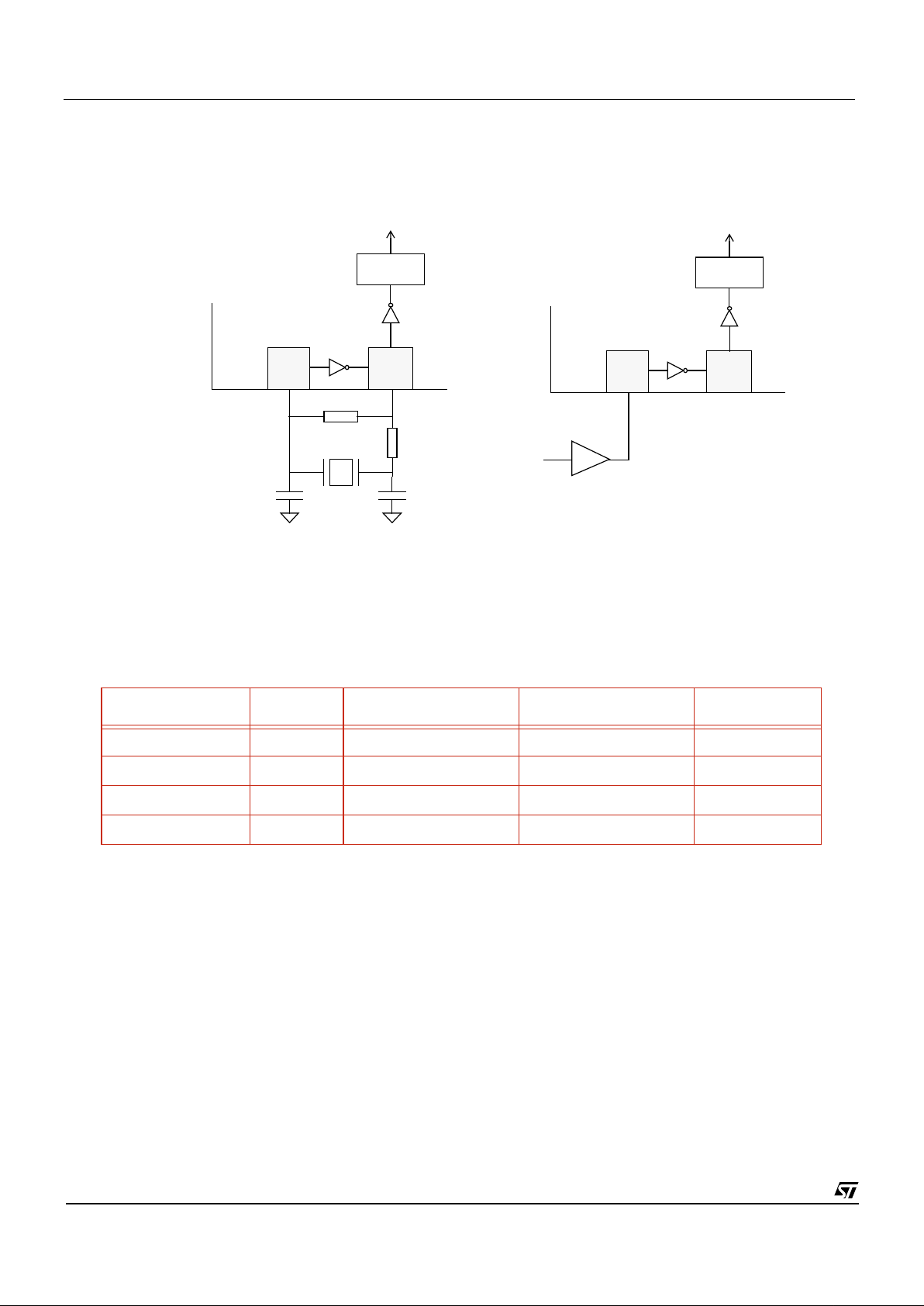
3.3 System Clock Generation
VV5301/VV6301 generates a system clock when a quartz crystal or ceramic resonator circuit is connected to the CLKI and CLKO
pins. The device can also be driven directly from an external clock source driving CLKI.
Figure 4 : Camera Clock Source
For greater flexibility the input frequency can be divided by 1, 2, 4 or 8 to select the pixel clock frequency. Two bits in the clock
division register in the serial interface select the input clock frequency divisor. The table below gives the different frame rates that
can be selected, when CLKI = 14.318MHz, for up to 30frames per second, for each divisor.
3.4 Calculating Sensor Framerate
The VV5301/VV6301 frame rate depends upon:
• the frequency of the system clock (CLKI)
• the ADC conversion accuracy (8-bit)
• the internal clock divisor selected (1, 2, 4, or 8)
• the output format is a constant 2
User can set their own values for CLKI and also the clock divisor setting. The frame rate is determined as follows
An example is given with a clock input of 14.318MHz, 160 x120 (164 x 124) image format, 8-bit ADC conversion rate and a clock
divisor of 2.
1. Determine clock input (CLKI) frequency - 14.318MHz
2. Pixel period = (divisor x conversion factor x output format factor) / CLKI
CLKI (MHz) Divisor Pixel Period (us) Frame Rate Comments
14.318 1 1.1175 29.99 default
14.318 2 2.235 15.01
14.318 4 4.47 7.5
14.318 8 8.94 3.75
Table 3 : Clock Division (60Hz Video Mode)
X1
C2
C1
R1
32 31
CKIN
CKOUT
CLK
VV5301/VV6301
3231
CKIN
CKOUT
CMOS Driver
Clock
Source
R2
C1=C2=47pF
R1=1MΩ
R2=510Ω
X1= 14.318MHz (up to 30fps)
17.73MHz (up to 25fps)
CLOCK
DIVISION
CLK
CLOCK
DIVISION
VV5301/VV6301
Page 11

CMOS Sensor; Customer Datasheet, Rev 3.0, 25 September 2000 VV5301 & VV6301
11/50
cd5301_6301f-3-0.fm
Commercial in confidence
Clock divisor = 1, 2, 4 or 8.
Conversion factor = 8 for 8-bit ADC accuracy
Output format factor is 2
Example: Pixel period = (2 x 8 x 2) / 14.318MHz = 2.235µs
3. Line period = (no. of visible pixels + line overhead) x pixel period
The number of visible pixels per line is 160. The interline pixel period overhead (including the 4 border pixels that can be enabled
to qualify extra video information) is mode dependent, 43 pixel periods for 60Hz mode or 141 pixel periods for 50Hz mode.
Example: Line period = (160 + 43) x 2.235µs = 453.705µs
4. Frame period = (no. of visible lines + frame overhead) x line period
For the purposes of calculating the effective frame rate the number of active lines is assumed to be fixed at 120. The frame
overhead (which includes the 4 border lines that can be enabled to qualify extra video information) has a constant value of 27 line
periods.
Example: Frame period = (120 + 27) x 453.705µs = 66.694ms
giving a frame rate = 1 / frame period = 15 frames per second
Page 12
VV5301 & VV6301 Auto Black Calibration
cd5301_6301f-3-0.fm
Commercial in confidence
12/50
4. Auto Black Calibration
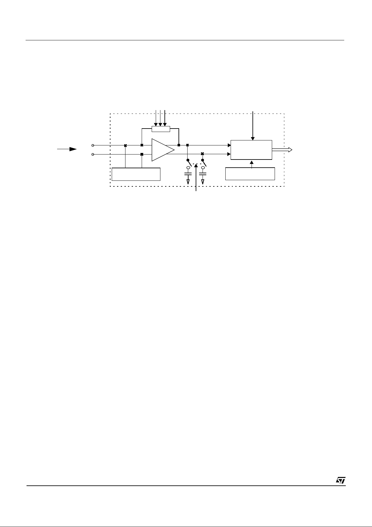
Black calibration is used to remove voltage offsets that cause shifts in the black level of the video signal. The VV5/6301 is
equipped with an automatic function that continually monitors the output black level and calibrates if it has moved out of range.
The signal is corrected using two “Black-Cal” DACs, B0 and B1, shown below
Figure 5 : Block Diagram of Black Calibration System
Black calibration can be split into two stages, monitor (1 cycle over 2 lines) and update (3 cycles, each cycle takes 2 lines).
During the monitor phase the current black level is compared against two threshold values. If the current value falls outside the
threshold window then an update cycle is triggered. The update cycle can also be triggered by a change in the gain applied to
sensor core or via the serial interface.
4.1 Monitor Procedure
The decision on when to re-calibrate the black level is made during the first cycle through the black reference lines. The decision
area for the black monitor is by default the last 16 pixels of the middle 128 pixels of the second designated black line, line 2.
However if this set of pixels fail to give a “good” black level then it is possible to use the penultimate group of 16 pixels.
The black reference pixels are summed, averaged and then compared with the monitor window. If the average falls outside the
window a flag is then set to force a re-calibration of the DAC values.
4.2 Update
The black calibration update sequence requires three phases and is performed over the remaining black lines at the start of the
video field, lines 3 to 8. During the first phase initial B0 DAC calibration is performed. In the second, the B1 DAC is calibrated
within the limitation of its step size. In the final phase the black level is fine tuned by re-calibrating the BO DAC.This is due to the
B1 DAC having a relatively coarse step size when high gain is applied.
The two calibration phases for the B0 DAC differ in that the first time it is calibrated it is working on common mode data. During
the final phase the B0 DAC is fine-tuned using black reference pixels.
G2:0]
DATA[7:0]
S/H
amp
ADCLK
Blk
Sig
8bit ADC
B1 DAC (8bit)
B0 DAC (8bit)
Vsig
Vref
From Sensor
ADSAM
Array
to digital logic
Page 13

CMOS Sensor; Customer Datasheet, Rev 3.0, 25 September 2000 VV5301 & VV6301
13/50
cd5301_6301f-3-0.fm
Commercial in confidence
5. Exposure Control
5.1 Calculating Exposure Period
The exposure time, comprising coarse and fine components, for a pixel and the analogue gain are programmable via the serial
interface.
The coarse exposure value sets the number of complete lines a pixel exposes for, while the fine exposure sets the number of
additional pixel clock cycles a pixel integrates for. The sum of the two gives the overall exposure time for the pixel array.
Exposure Time = ((Coarse setting x Line Period) + (Fine setting)) x (CLKI clock period) x Clock Divider Ratio
note1
note1: Clock Divider Ratio = 1/(Basic Clock Division * Optional Pixel Clock Divisor)
5.2 Automatic Exposure Control
With automatic exposure control selected VV5301/VV6301 uses a complex algorithm to automatically set the exposure value for
the current scene. When combined with clock control and gain control the VV5301/VV6301 can operate over a very wide range of
illumination levels.
5.3 Updating Exposure, Gain and Clock Division Settings
Although the user can write a new exposure, gain or clock division parameter at any point within the field the sensor will only
consume these new external values at a certain point. The exception to this behaviour are when the user has selected immediate
update of gain If the user has selected the former then the new gain value will be applied as soon as the serial interface message
has completed. The fine and coarse exposure values are always written in a “timed” manner. There are two “update pending”
flags available to the user (see Status0 reg[2] for details) that allows the user to detect when the sensor has consumed one of the
timed parameters. In the next section of this document we will detail all the timed parameters and describe when they are
updated.
It is important to realise that there is a 1 frame latency between a new exposure value being applied to the sensor array and the
results of this new exposure value being read-out. The same latency does not exist for the gain value. To ensure that the effect of
the new exposure and gain values are coincident the sensor delays the application of the new gain value by approximately one
frame relative to the application of the new exposure value.
If the user is using the autoincrement option in the serial interface when writing a new series of exposure/gain and clock division
parameters then it is important to ensure that the sensor receives the complete message bunch before updating any of the
parameters. It is also important that the timed parameters are updated in the correct order, we will discuss this fully in the next
section. If an autoincrement message sequence is in progress but we have reached the point in the field timing where the gain
value would normally be updated, we actually inhibit the update. We inhibit the update to ensure that the gain change is not
passed to the sensor while a change in the exposure is still pending.
5.4 Clock Control
The system clock can be divided down internally to extend the operating range of VV5301/VV6301 by allowing longer exposure
times. The clock divisor options are as follows:
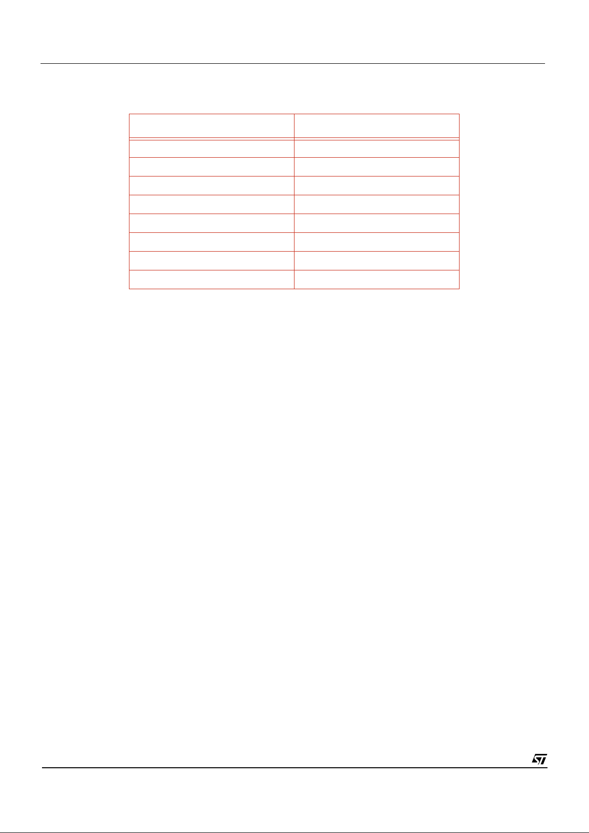
If the user increases the clock divisor setting then the effective exposure period is also increased.
Clock divisor register Effective clock division
2’b00 1
2’b01 2
2’b10 4
2’b11 8
Table 4 : Available clock division
Page 14
VV5301 & VV6301 Exposure Control
cd5301_6301f-3-0.fm
Commercial in confidence
14/50
5.5 Gain Setting
An external gain value can be written to the sensor as follows.
If the image is to dark and the exposure is already close to its maximum the automatic exposure algorithm will attempt to use
extra steps of gain to improve the image brightness. Each change applied by the internal algorithm will double the current value.
To compensate for this increase in gain the current exposure is set to half of the maximum value. This should ensure that the
user will not be aware of a step change in the scene brightness.
Similarly if the image is too bright and the integration period is short then gain will be reduced by one step (i.e. divide by two). As
before, the exposure value is set to half the maximum integration period. The exposure controller can then adjust the exposure
value as necessary to provide a correctly exposed image.
If the user disables the automatic exposure/gain controller then the extra gain settings detailed in Table 5 above are available.
Gain binary code Effective system gain
000 1.000
001 2.000
010 1.333
011 4.000
100 1.143
101 2.667
110 1.600
111 8.000
Table 5 : Gain settings
Page 15

CMOS Sensor; Customer Datasheet, Rev 3.0, 25 September 2000 VV5301 & VV6301
15/50
cd5301_6301f-3-0.fm
Commercial in confidence
6. Timed Serial Interface Parameters
The previous section, Exposure Control, introduced the concept of a “timed parameter”, that is information that is written via the
serial interface but will not be used immediately by the sensor, rather there will be a delay before the information is passed to the
internal registers (referred to as the working registers) from the serial interface registers (referred to as the shadow registers). It is
the contents of the working registers that will determine sensor behaviour.
6.1 Listing and Categorizing the Parameters
The timed parameters are split into 2 categories as follows:
• fine and coarse exposure
• gain
There is a “pending” flag for each of the above categories. These flags are stored in Status0 Register[2] in bits [0] and [2]. If one
of the flags is high this indicates that the working register/s controlled by that flag have yet to be updated from the according
shadow register/s. This feedback information could be useful if a user is, for example, attempting to write an external exposure
controller. The status of the pending flags allows accurate timing of the serial interface communications.
6.1.1 Fine and Coarse Exposure
The exposure category comprises registers[32,33] and [34,35].
6.1.2 Gain
The gain category simply comprises register[36].
6.2 Timed Parameter Update Points
The timed parameter categories are updated as follows:
note: We refer to odd and even fields in the table below. Each field is identical in length but we have to be able to differentiate
between fields to enable correct updating of register parameters.
If a change in exposure and gain are pending at the same time then the exposure value will be updated first followed by the gain.
This will ensure image illumination continuity from field to field.
Timed parameter category Updated point
fine and coarse exposure During the interline period between the last line of the odd field and the first
line of the even field.
gain During the interline period between line 143 and line 144 in the even field.
Table 6 : Timed Parameter Update Points
Page 16
VV5301 & VV6301 Digital Video Interface Format
cd5301_6301f-3-0.fm
Commercial in confidence
16/50
7. Digital Video Interface Format
The video interface consists of a bidirectional, tri-stateable 5-wire data bus. The nibble transmission is synchronised to the rising
edge of the system clock.
Digital video data is 8 bits per sample in VV5301 and VV6301. The data can be transmitted in the following ways:
• A single 8 bit byte over 8 output wires
note
.
• A series pair of 4-bit nibbles, most significant nibble first, on 4 wires.
7.1 Embedded control data
To distinguish the control data from the sampled video data all control data is encapsulated in embedded control sequences.
These are 6 bytes long and include a combined escape/sync character sequence, 1 control byte (the ‘command byte’) and 2
bytes of supplementary data.
To minimise the susceptibility of the embedded control data to random bit errors redundant coding techniques have been used to
allow single bit errors in the embedded control words to be corrected. However, more serious corruption of control words or the
corruption of escape/sync characters cannot be tolerated without loss of sync to the data stream. To ensure that a loss of sync is
detected a simple set of rules has been devised. The four exceptions to the rules are outlined below:
1. Data containing a command word that has two bit errors.
2. Data containing two ‘end of line’ codes that are not separated by a ‘start of line’ code.
3. Data preceding an ‘end of field’ code before a start of frame’ code has been received.
4. Data containing line that do not have sequential line numbers (excluding the ‘end of field’ line).
If the receiving software or hardware detects one of these violations then it should abandon the current field of video
7.1.1 The combined escape and sync character
Each embedded control sequence begins with a combined escape and sync character that is made up of three words. The first
two of these are FF
H
FFH- constituting two words that are illegal in normal data. The next word is 00H - guaranteeing a clear
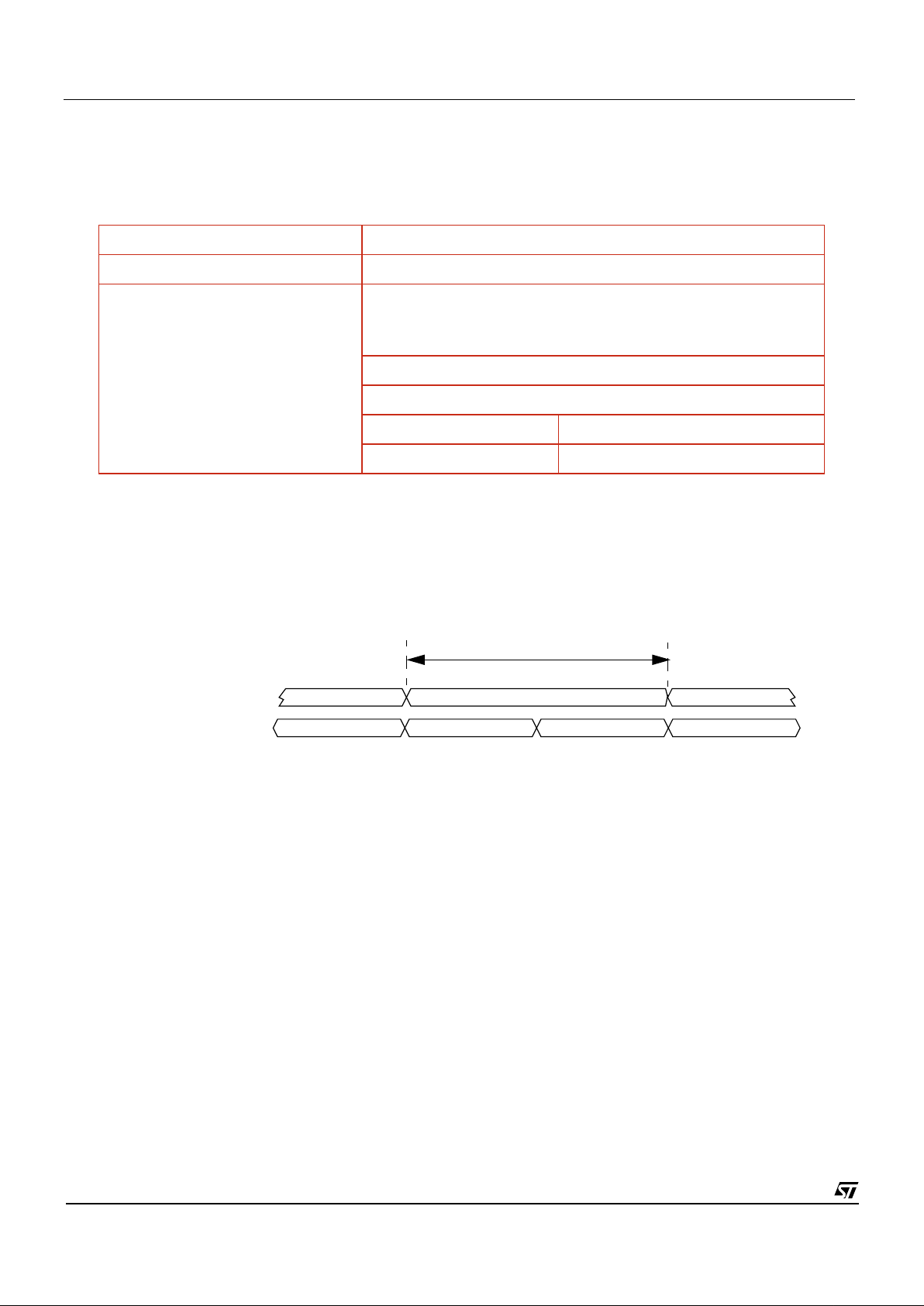
Read-out Order Progressive Scan (Non-interlaced)
Form of encoding Uniformly quantised, PCM, 8/10 bits per sample
Correspondence between video signal
levels and quantisation levels:
The internal10-bit pixel data is clipped to ensure that 0
H
and 3FFH (5
Wire) or FF
H
(4/8 Wire) values do not occur when pixel data is being
output on the data bus.
VV5301/VV6301
8-Bit Data
Pixel Values 1 to 254
Black Level 16
Figure 6 : Output Modes
4 - wire Output Mode
D7,D6,D5,D
4
D3,D2,D1,D
0
D3,D2,D1,0
2
D7,D6,D5,D
4
8-bit Pixel Data
8- wire Output Mode
D7,D6,D5,D4,D3,D2,D1,D
0
D7,D6,D5.............D2,D1,D
0
Page 17
CMOS Sensor; Customer Datasheet, Rev 3.0, 25 September 2000 VV5301 & VV6301
17/50
cd5301_6301f-3-0.fm
Commercial in confidence
signal transition that allows a video processor to determine the position of the word boundaries in the serial stream of nibbles.
Combined escape and sync characters are always followed by a command byte - making up the four byte minimum embedded
control sequence.
7.1.2 The command word
The byte that follows the combined escape/sync characters defines the type of embedded control data. Three of the 8 bits are
used to carry the control information, four are ‘parity bits’ that allow the video processor to detect and correct a certain level of
errors in the transmission of the command words, the remaining bit is always set to 1 to ensure that the command word never has
the value 00
H
. The coding scheme used allows the correction of single bit errors (in the 8-bit sequence) and the detection of 2 bit
errors.The even parity bits are based on the following relationships:
1. An even number of ones in the 4-bit sequence (C
2
, C1, C0 and P0).
2. An even number of ones in the 3-bit sequence (C
2
, C1, P1).
3. An even number of ones in the 3-bit sequence (C
2
, C0, P2).
4. An even number of ones in the 3-bit sequence (C
1
, C0, P3).
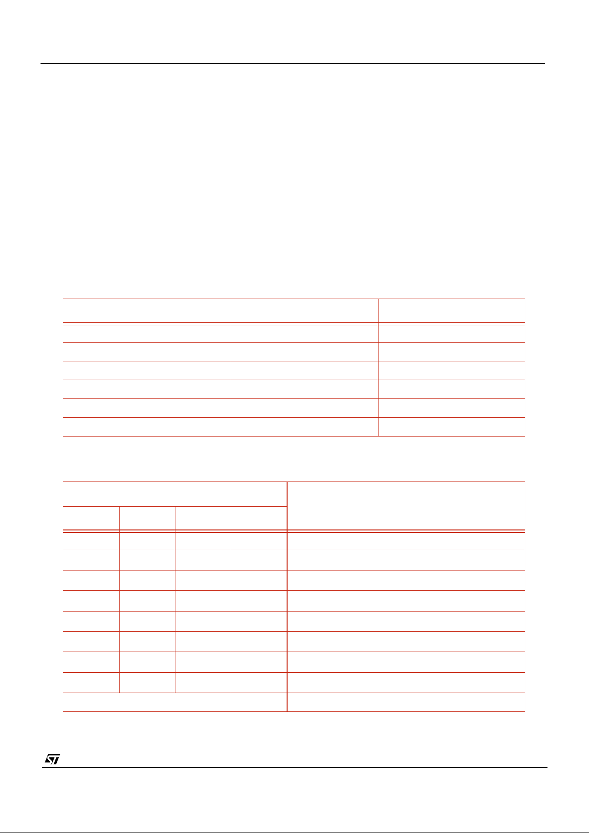
Table 8 shows how the parity bits maybe used to detect and correct 1-bit errors and detect 2-bit errors.
Line Code Nibble XH(1 C2 C1C0) Nibble YH(P3 P2 P1 P0)
End of Line 10002(8H) 00002 (0H)
Blank Line (BL) 1001
2(9H
) 11012 (DH)
Black line (BK) 1010
2(AH
) 10112 (BH)
Visible Line (VL) 1011
2(BH
) 01102 (6H)
Start of Field (SOF) 1100
2(CH
) 01112 (7H)
End of Field (EOF) 1101
2(DH
) 10102 (AH)
Table 7 : Embedded Line Codes (for 4 wire output mode)
Parity Checks
Comment
P
3
P
2
P
1
P
0
✔✔✔✔Code word un-corrupted
✔✔✔✘P
0
corrupted, line code OK
✔✔✘✔P
1
corrupted, line code OK
✔✘✔✔P
2
corrupted, line code OK
✘✔✔✔P
3
corrupted, line code OK
✘✘✔✘C
0
corrupted, invert sense of C
0
✘✔✘✘C1 corrupted, invert sense of C
1
✔✘✘✘C2 corrupted, invert sense of C
2
All other codes 2-bit error in code word.
Table 8 : Parity Checking
Page 18

VV5301 & VV6301 Digital Video Interface Format
cd5301_6301f-3-0.fm
Commercial in confidence
18/50
7.2 8-Wire Parallel Mode
If this output mode is selected then the 8-bit pixel data is output on pins DATA[7:0]. The data is valid on the falling edge of the
pixel qualification clock, QCK.
7.3 4-Wire Parallel Mode
If the 4-Wire parallel mode is selected then a pixel value is output over 2, 4-wire nibbles transmitted over pins DATA[7:4]. A falling
edge on QCK will sample a data nibble.
Page 19
CMOS Sensor; Customer Datasheet, Rev 3.0, 25 September 2000 VV5301 & VV6301
19/50
cd5301_6301f-3-0.fm
Commercial in confidence
7.4 Video Frame Composition
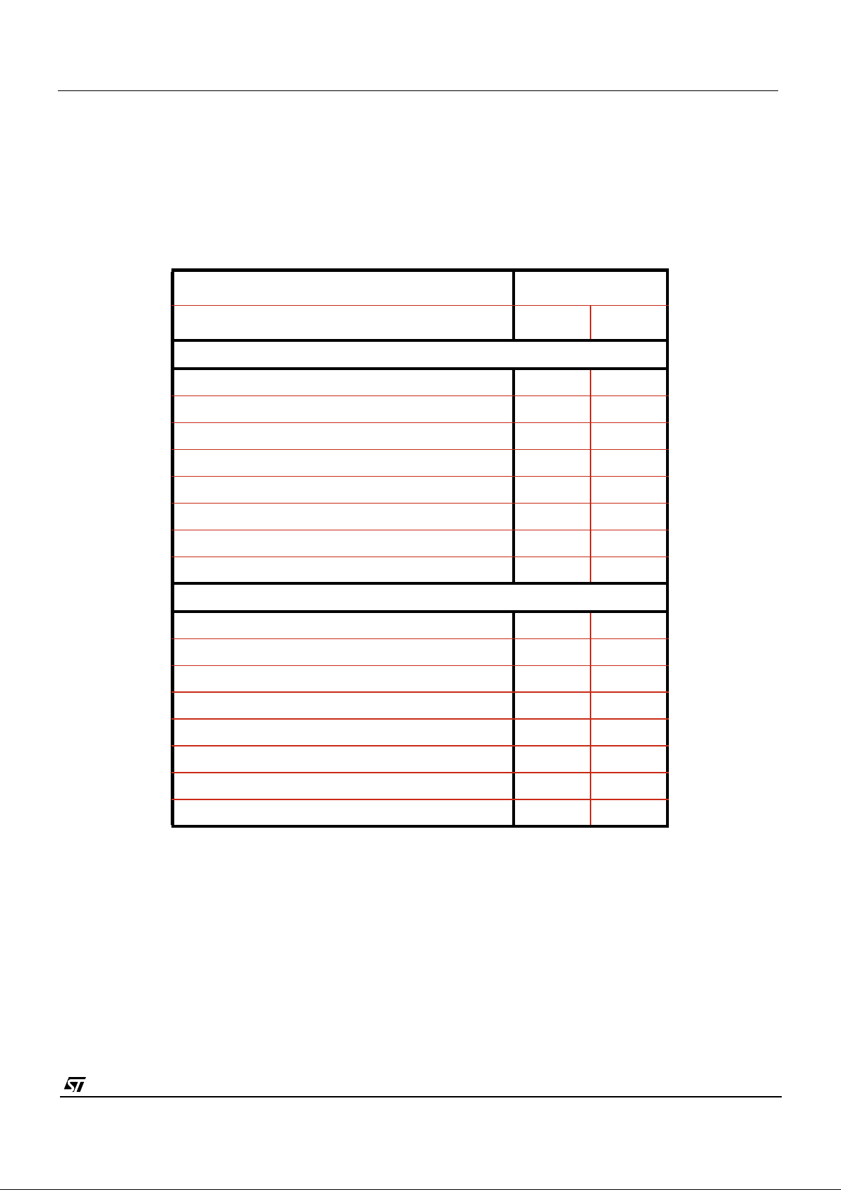
Each frame of video sequence comprises 2 fields. Each field of data is constructed of the following sequence of data lines.
1. A start of field line
2. A number of black lines
3. A number of blank (or dark) lines
4. A number active video lines
5. An end of field line
6. A number of blank or black lines
Each line of data starts with an embedded control sequence that identifies the line type (as outlined in). The control sequence is
then followed by two bytes that contain a coded line number. The line number sequences starts with the start-of-frame line at 00
H
and increments one per line up until the end-of-frame line. Each line is terminated with an end-of-line embedded control
sequence. The line start embedded sequences must be used to recognise visible video lines as a number of null bytes may be
inserted between successive data lines.
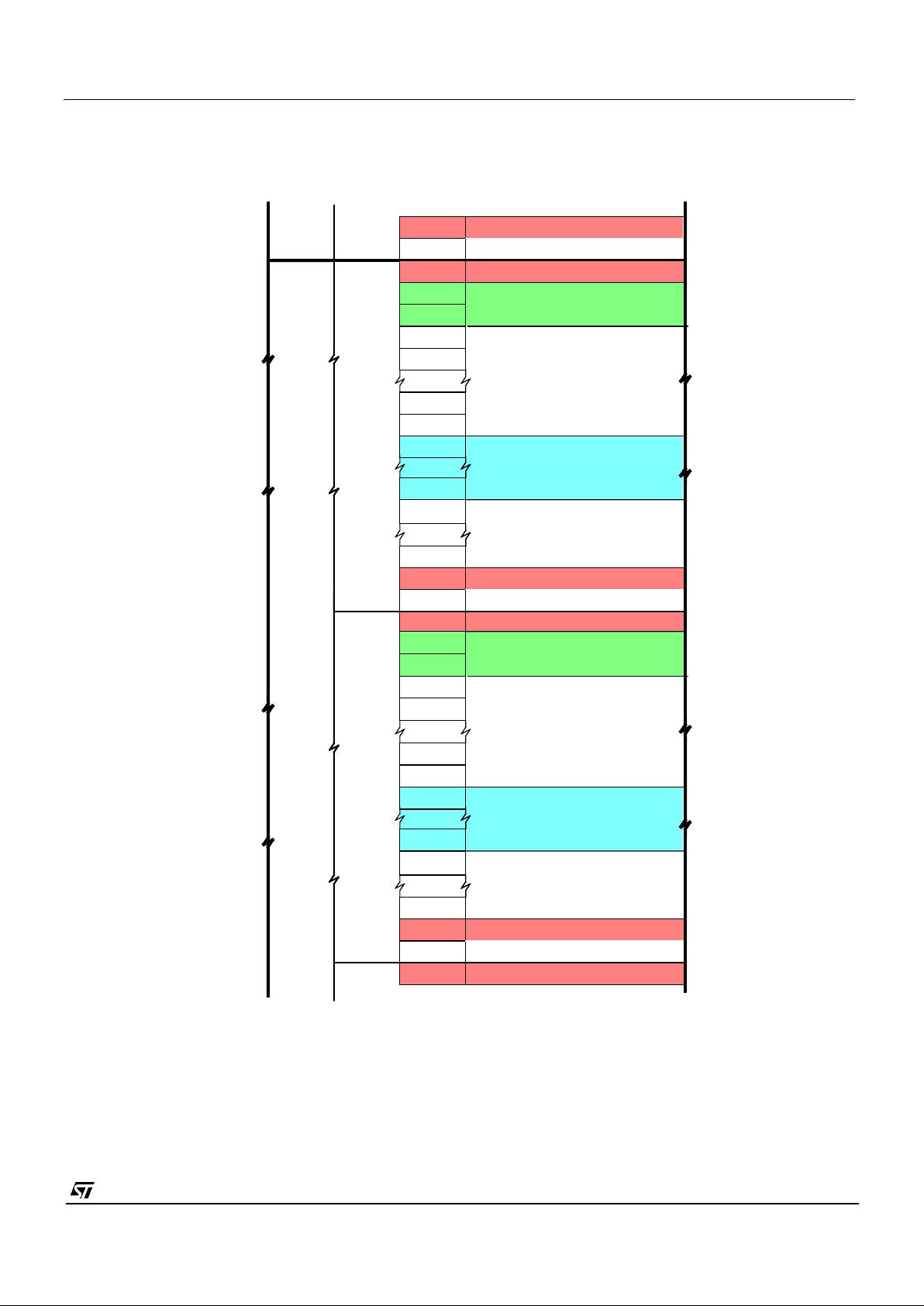
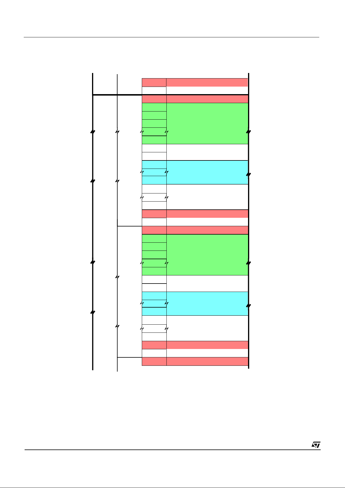
There are two figures (Figure 7 - Figure 8) on the following pages that show line type field construction.
7.4.1 Blank lines
In addition to padding between data lines, actual blank data lines may appear in the positions indicated above. These lines begin
Video Format QSIF
Extra Black Lines On Off
1st Field
Start of Field Line 1 1
Black Lines 8 2
Blanking Lines 2 8
Active Video lines 124 124
Blanking Lines 10 10
End of Field Line 1 1
Blanking Lines 1 1
Total 147 147
2nd Field
Start of Field Line 1 1
Black Lines 8 2
Blanking Lines 2 8
Active Video lines 124 124
Blanking Lines 10 10
End of Field Line 1 1
Blanking Lines 1 1
Total 147 147
Table 9 : Field and Frame Composition
Page 20

VV5301 & VV6301 Digital Video Interface Format
cd5301_6301f-3-0.fm
Commercial in confidence
20/50
with start-of-blank-line embedded control sequences and are constructed identically to active video lines except that they will
contain only blank bytes, 07
H
, (expressed as 01CH in 10bit form).
7.4.2 Black line timing
The black lines (which are used for black calibration) are identical in structure to valid video lines except that they begin with a
start-of-black line code and contain information from the sensor black lines.
The user can opt to enable extra black lines up to a maximum of 8. The black calibration algorithm always has access to the data
contained within these lines whether they are externally enabled or not.
Page 21
CMOS Sensor; Customer Datasheet, Rev 3.0, 25 September 2000 VV5301 & VV6301
21/50
cd5301_6301f-3-0.fm
Commercial in confidence
Figure 7 : Field and Frame Formats - Extra Black Lines Off
Frame = 294 Lines
2 Black Lines
Start Of 1st Field Line
End Of 1st Field Line
Blanking Lines
124 Visible Lines
Blanking Line
1st Field = 147 Lines
1
0
2
3
9
10
11
135
145
146
Blanking Lines
134
144
Start Of 1st Field Line
End Of 1st Field Line
124 Visible Lines
Blanking Line
0
11
135
145
146
Blanking Lines
134
144
2nd Field = 147 Lines
Start Of 1st Field Line0
End Of 1st Field Line
Blanking Line
145
146
4
2 Black Lines
Blanking Lines
1
2
3
9
10
4
Page 22
VV5301 & VV6301 Digital Video Interface Format
cd5301_6301f-3-0.fm
Commercial in confidence
22/50
Figure 8 : Field and Frame Formats - Extra Black Lines On
Frame = 294 Lines
8 Black Lines
Start Of 1st Field Line
End Of 1st Field Line
Blanking Lines
124 Visible Lines
Blanking Line
1st Field = 147 Lines
1
0
2
3
9
10
11
135
145
146
8
Blanking Lines
134
144
8 Black Lines
Start Of 1st Field Line
End Of 1st Field Line
Blanking Lines
124 Visible Lines
Blanking Line
1
0
2
3
9
10
11
135
145
146
8
Blanking Lines
134
144
2nd Field = 147 Lines
Start Of 1st Field Line0
End Of 1st Field Line
Blanking Line
145
146
Page 23

CMOS Sensor; Customer Datasheet, Rev 3.0, 25 September 2000 VV5301 & VV6301
23/50
cd5301_6301f-3-0.fm
Commercial in confidence
7.5 Qualifying the Output Data
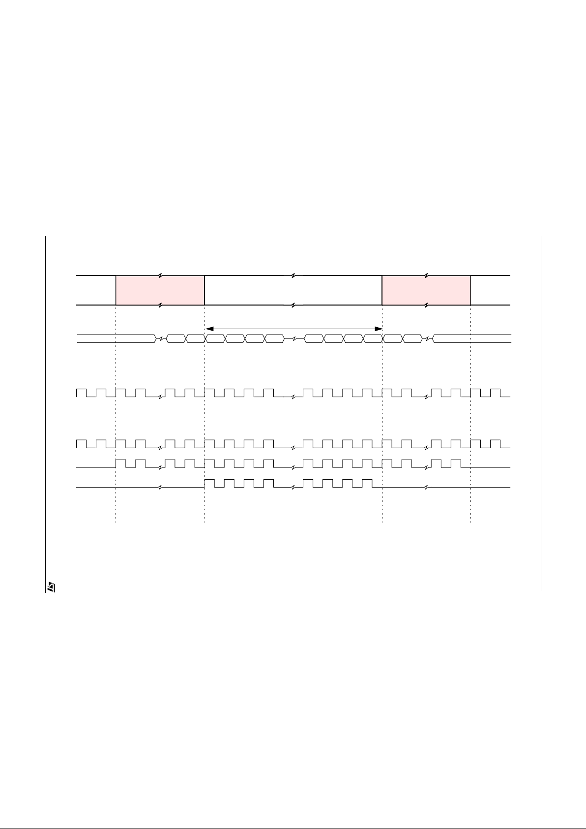
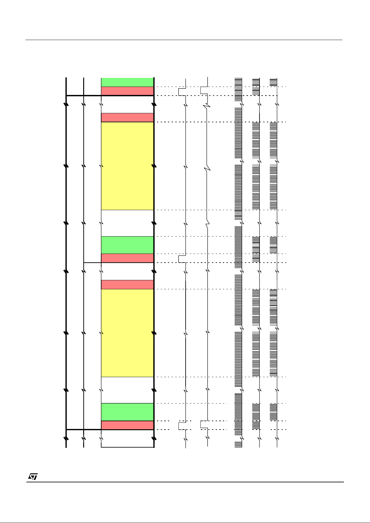
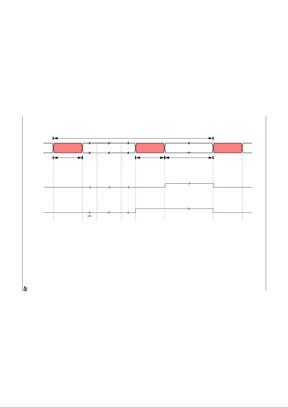
Data is output from VV5301/VV6301 in a continuous stream. By utilizing signals, like FST, and key events, like the start of a line
or the end of line, the user can sample and display the image data. QCK is used to sample the data, as described in the previous
section.
Different periods of the frame can be qualified by QCK. The options, which are selected via setup register4 in the serial interface,
are as follows:
1. QCK disabled, no data qualified (default)
2. QCK free running, all data qualified
3. QCK qualifies image data only, to include data on black lines currently enabled
4. QCK qualifies embedded control sequences as well as image data. The status line data is also qualified with this option.
7.5.3 Frame Start Signal, FST
There are 3 modes of operation for the FST pin programmable via the serial interface:
1. FST disabled, (default).
2. FST enabled, qualifies
3. Shutter/Electronic Flash Synchronisation Signal - FST rises a the start of the video data in the first black/blank line after the
EOF line and falls at the end of data in the SOF line.
The FST output is tri-stated either when OEB is driven high or via the appropriate control bit in the serial interface, (see
data_format register[22]).
Page 24
VV5301 & VV6301 Digital Video Interface Format
cd5301_6301f-3-0.fm
Commercial in confidence
24/50
End of Active Video
(EAV)
Start of Active Video
(SAV)
Pixel Data
Figure 9 : Qualification of Output Data (Border Rows and Columns Enabled).
Video Data
F
H
Line Format
4-wire Nibble Output Mode - D[3:0]
D1D
0
F
H
FHF
H
PMPLPMP
L
PMPLPMP
L
Crystal Clock or external clock applied to CKI
PM = Pixel Value - Most Significant Nibble, PL = Pixel Value - Least Significant Nibble, P = 8-bit Pixel Value
Qualification Clock, QCK
(i) Free running
(ii) Control sequences and Pixel Data
(iii) Pixel Data only
Page 25
CMOS Sensor; Customer Datasheet, Rev 3.0, 25 September 2000 VV5301 & VV6301
25/50
cd5301_6301f-3-0.fm
Commercial in confidence
Figure 10 : Frame/Field Level Timings for FST and QCK.
Start of Field
Black Lines
Blanking Lines
Visible Lines
End of Field
Blanking Lines
Blanking Lines
Start of Field
2nd Field
1 Frame
Start of Field
Black Lines
Blanking Lines
Visible Lines
End of Field
Blanking Lines
1st Field
Frame/Field Format:
QCK:
(iii) Data Only
(ii) Control plus Data
(i) Free Running
(i) FST
(i) sno
Page 26
VV5301 & VV6301 Digital Video Interface Format
cd5301_6301f-3-0.fm
Commercial in confidence
26/50
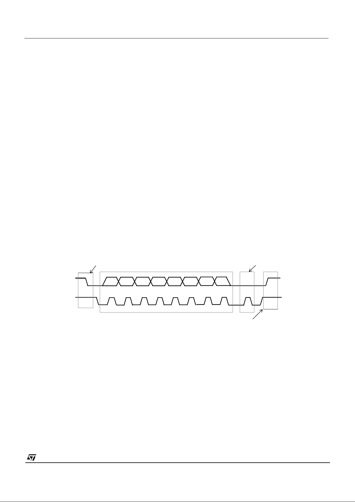
Figure 11 : Line Level Timings for FST.
Video
Data
Start of Active
Video (SAV)
EAV
Inter-line Period (DataBus = FH)
End ofActive Video
(EAV)
FST Pin:
(ii) Synchronisation Output - SNO
(i) Frame start pulse - qualifies status line information
End ofActive Video
(EAV)
6 Pixels 168Pixels6 Pixels
1 Line
Video Data
Page 27
CMOS Sensor; Customer Datasheet, Rev 3.0, 25 September 2000 VV5301 & VV6301
27/50
cd5301_6301f-3-0.fm
Commercial in confidence
8. Serial Control Bus
8.1 General Description
Writing configuration information to the video sensor and reading both sensor status and configuration information back from the
sensor is performed via the 2-wire serial interface.
Communication using the serial bus centres around a number of registers internal to the video sensor. These registers store
sensor status, set-up, exposure and system information. Most of the registers are read/write allowing the receiving equipment to
change their contents. Others (such as the chip id) are read only.
The main features of the serial interface include:
• Broad-cast address to ease setting up multiple camera configurations.
• Variable length read/write messages.
• Indexed addressing of information source or destination within the sensor.
• Automatic update of the index after a read or write message.
• Message abort with negative acknowledge from the master.
• Byte oriented messages.
The contents of all internal registers accessible via the serial control bus are encapsulated in each start-of-field line.
8.2 Serial Communication Protocol
The co- processor or host must perform the role of a communications master and the camera acts as either a slave receiver or
transmitter.The communication from host to camera takes the form of 8-bit data with a maximum serial clock video processor
frequency of up to 100 kHz. Since the serial clock is generated by the bus master it determines the data transfer rate. Data
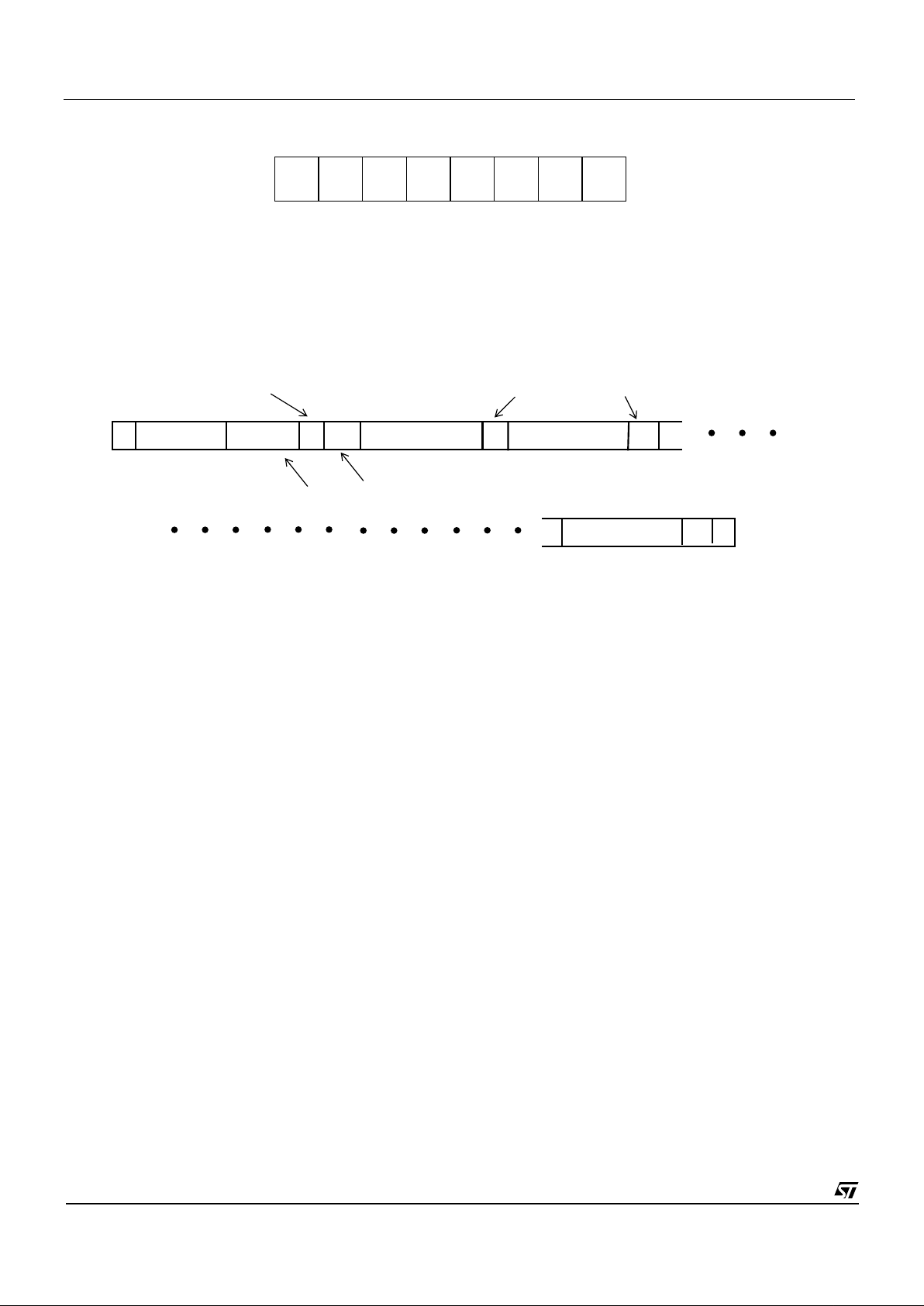
transfer protocol on the bus is illustrated in Figure 12.
8.3 Data Format
Information is packed in 8-bit packets (bytes) always followed by an acknowledge bit. The internal data is produced by sampling
sda
at a rising edge of
scl
. The external data must be stable during the high period of
scl
. The exceptions to this are
start
(S) or
stop
(P) conditions when
sda
falls or rises respectively, while
scl
is high.
A message contains at least two bytes preceded by a
start
condition and followed by either a
stoporrepeated start, (Sr)
followed
by another message.
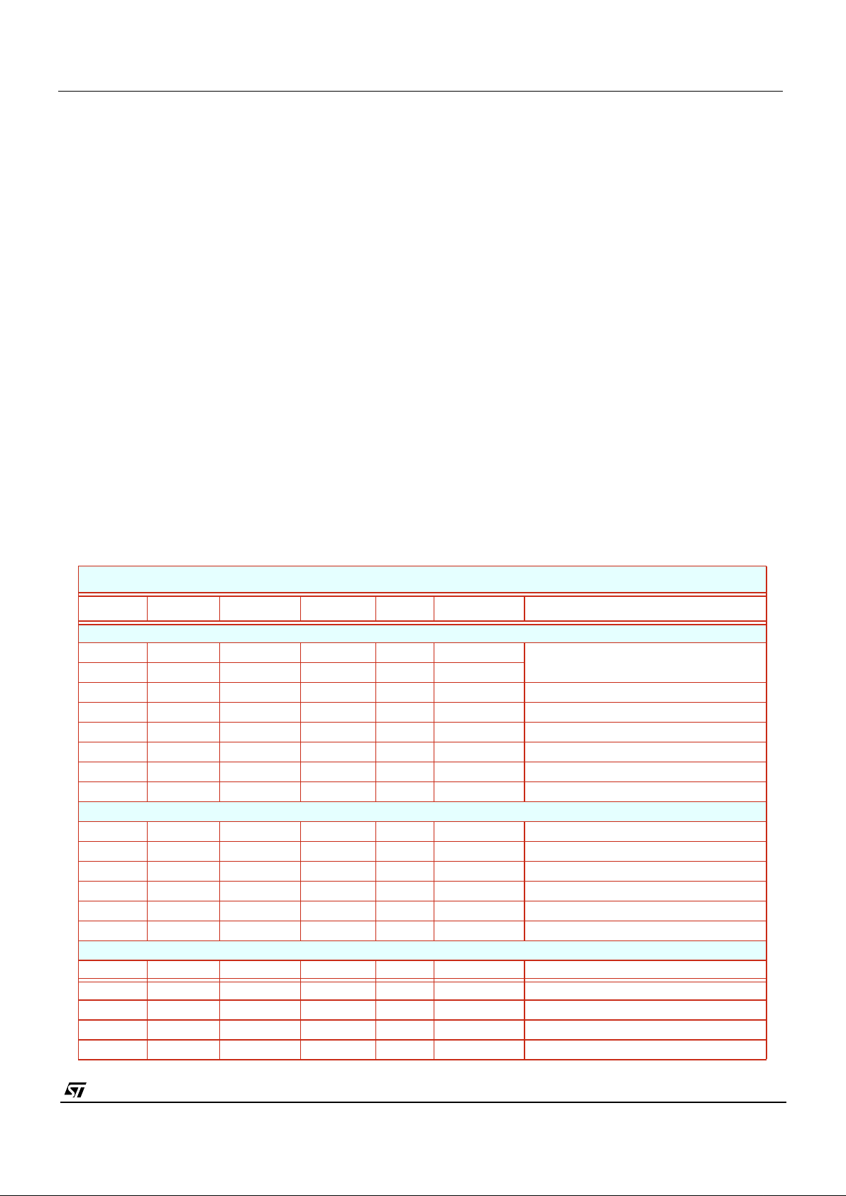
The first byte contains the device address byte which includes the data direction
read,
(r)
, ~write
, (~w), bit. The lsb of the address
byte indicates the direction of the message. If the lsb is set high then the master will read data from the slave and if the lsb is reset
low then the master will write data to the slave. After the
r, ~w
bit is sampled, the data direction cannot be changed, until the next
address byte with a new
r, ~w
bit is received.
12
7
8
A
Start condition
Stop condition
SDA
SCL
Acknowledge
P
S
3 4 56
Address or data byte
MSB LSB
Figure 12 : Serial Interface Data Transfer Protocol
Page 28
VV5301 & VV6301 Serial Control Bus
cd5301_6301f-3-0.fm
Commercial in confidence
28/50
The byte following the address byte contains the address of the first data byte (also referred to as the
index
). The serial interface
can address up to 128, byte registers. If the msb of the second byte is set the automatic increment feature of the address index is
selected.
8.4 Message Interpretation
All serial interface communications with the sensor must begin with a
start
condition. If the
start
condition is followed by a valid
address byte then further communications can take place. The sensor will acknowledge the receipt of a valid address by driving
the
sda
wire low. The state of the
read/~write
bit (lsb of the address byte) is stored and the next byte of data, sampled from
sda,
can be interpreted.
During a write sequence the second byte received is an address index and is used to point to one of the internal registers. The
msbit of the following byte is the
index auto increment
flag. If this flag is set then the serial interface will automatically increment
the index address by one location after each slave acknowledge. The master can therefore send data bytes continuously to the
slave until the slave fails to provide an acknowledge or the master terminates the write communication with a
stop
condition or
sends a
repeated start, (Sr)
. If the auto increment feature is used the master does
not
have to send indexes to accompany the
data bytes.
As data is received by the slave it is written bit by bit to a serial/parallel register. After each data byte has been received by the
slave, an acknowledge is generated, the data is then stored in the internal register addressed by the current index.
During a read message, the current index is read out in the byte following the device address byte. The next byte read from the
slave device are the contents of the register addressed by the current index. The contents of this register are then parallel loaded
into the serial/parallel register and clocked out of the device by
scl.
At the end of each byte, in both read and write message sequences, an acknowledge is issued by the receiving device. Although
VV5301/VV6301 is always considered to be a slave device, it acts as a transmitter when the bus master requests a read from the
sensor.
At the end of a sequence of incremental reads or writes, the terminal index value in the register will be one
greater
the last
location read from or written to. A subsequent read will use this index to begin retrieving data from the internal registers.
A message can only be terminated by the bus master, either by issuing a stop condition, a repeated start condition or by a
negative acknowledge after reading a complete byte during a read operation.
0 0 1 0 0 0 0
Figure 13 : VV5301/VV6301’s Serial Interface Address
R/W
S
address[7:1]
R
/Wbit
A
DATA[7:0]
A
Sensor acknowledges valid address
Acknowledge from slave
INDEX[6:0]INC
P
A
A
DATA[7:0]
[0]
address
Auto increment
Index bit
Figure 14 : Serial Interface Data Format
Page 29
CMOS Sensor; Customer Datasheet, Rev 3.0, 25 September 2000 VV5301 & VV6301
29/50
cd5301_6301f-3-0.fm
Commercial in confidence
8.5 The Programmers Model
There are 128, 8-bit registers within the camera, accessible by the user via the serial interface. They are grouped according to
function with each group occupying a 16-byte page of the location address space. There may be up to eight such groups,
although this scheme is purely a conceptual feature and not related to the actual hardware implementation, The primary
categories are given below:
• Status Registers (Read Only).
• Setup registers with bit significant functions.
• Exposure parameters that influence output image brightness.
• System functions and analog test bit significant registers.
Any internal register that can be written to can also be read from. There are a number of read only registers that contain device
status information, (e.g. design revision details).
Names that end with H or L denote the most or least significant part of the internal register. Note that unused locations in the H
byte are packed with zeroes.
STMicroelectronics sensors that include a 2-wire serial interface are designed with a common address space. If a register
parameter is unused in a design, but has been allocated an address in the generic design model, the location is referred to as
reserved
. If the user attempts to read from any of these
reserved or unused
locations a default byte will be read back. In
VV5301/VV6301 this data is 12
H
. A write instruction to a reserved (but unused) location is illegal and would not be successful as
the device would not allocate an internal register to the data word contained in the instruction.
A detailed description of each register follows. The address indexes are shown as decimal numbers in brackets [....] and are
expressed in decimal and
hexadecimal
respectively.
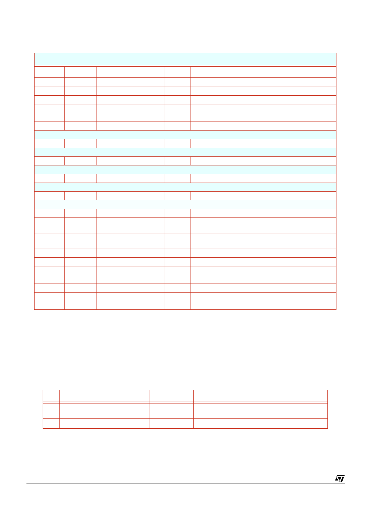
Serial Register Map for VV5301/VV6301
Index
10
Index
16
Name Length R/W Default Comments
Status Registers - [0-15]
0 0 DevH 8 RO 1100 0000
2
Reserved
1 1 DevL 8 RO 0001 0010
2
2 2 status0 8 RO 0000 1000
2
System status information
3 3 unused -
4-6 4-6 unused 8 RO
7 7 frame_av 8 RO Average value of pixels in a frame.
8-11 8-B unused 8 RO
12-15 C-F unused -
Setup Registers - [16-31]
16 10 setup0 8 R/W (27
H
) Configure the digital logic
17 11 setup1 8 R/W (70
H
) Configure the digital logic
18 12 setup2 8 R/W (1F
H
) Pixel counter reset value
19 13 setup3 8 R/W (0F
H
) Exposure control modes
20 14 setup4 8 R/W (00
H
) FST/QCK options
21-31 15 unused -
Exposure Registers - [32-47]
32 20 unused 33 21 fine 8 R/W 00
H
Fine exposure initially zero
34 22 unused 35 23 coarse 8 R/W 70
H
Coarse exposure
36 24 gain 8 R/W 00
H
Gain value
Page 30
VV5301 & VV6301 Serial Control Bus
cd5301_6301f-3-0.fm
Commercial in confidence
30/50
A detailed description of each register follows. The address indexes are shown as binary in brackets.
8.5.1 Status Registers - [0 - 15],
[0-F]
[0-1],
[0-1]
-[0-1],
[0-1]
- DeviceH and DeviceL
These registers provide read only information that identifies the sensor type that has been coded as a 12bit number and a 4bit
mask set revision identifier. The initial mask revision identifier is 0 i.e. 0000
2
. As the mask set is upgraded the revision identifier
will increase, i.e. the second mask set will be 0001
2
and so on. The device identification number for VVL301 is 301 i.e. 0001 0010
1101
2
.
37 25 clk_div 8 R/W 00
H
Clock division
38 26 gn_lim 8 R/W 07
H
Maximum allowable gain
39 27 tl 8 R/W 55
H
Lower exposure control threshold.
40 28 tc 8 R/W 64
H
Centre exposure control threshold.
41 29 th 8 R/W 73
H
Upper exposure control threshold.
42-47 2A-2F unused -
Colour Registers - [48-79]
48-79 30-4F reserved
Video Timing Registers - [80-103]
80-103 50-67 reserved
Text Overlay Registers - [104-107]
104-107 68-6B reserved
Serial Interface Autoload Registers - [108-111]
108-111 6C-6F reserved
System Registers - [112-127]
112 70 bdac 8 R/W Black Calibration setup
113 71 b0 8 RO Manual override of Black Calibration
DAC register, B0
114 72 b1 8 RO Manual override of Black Calibration
DAC register, B0
115 73 unused
116 74 tms 8 R/W Digital comparator threshold
117 75 unused
118 76 cr0 8 R/W
119 77 cr1 8 R/W
120 78 reserved
120-127 79-7F unused
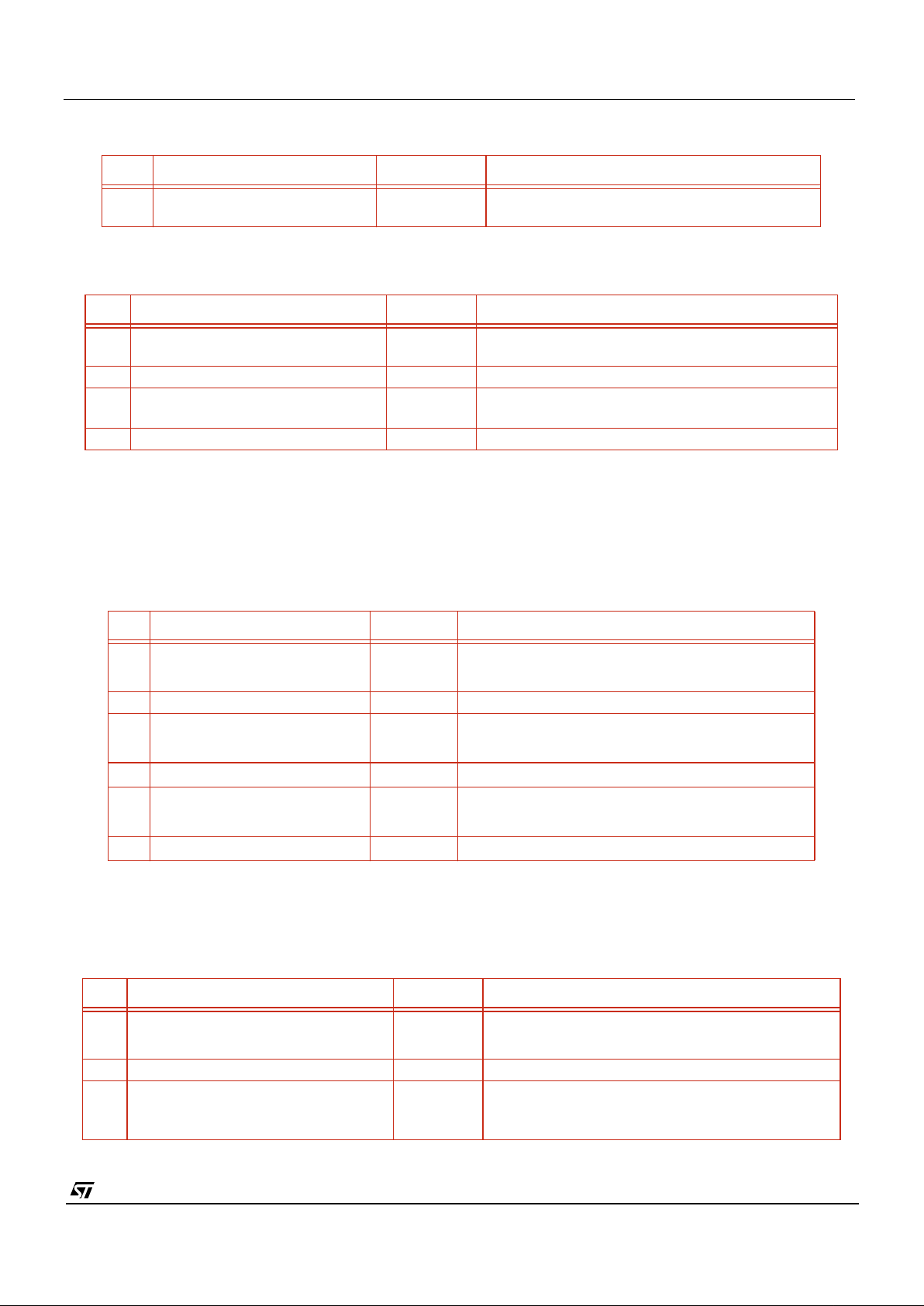
Bit Function Default Comment
7:4 Device type identifier 1101
2
Least significant 4bits of 12bit code identifying the
chip type.
3:0 Mask set revision identifier 0000
2
Table 10 : [0],
[0] -
DeviceL
Serial Register Map for VV5301/VV6301
Index
10
Index
16
Name Length R/W Default Comments
Page 31
CMOS Sensor; Customer Datasheet, Rev 3.0, 25 September 2000 VV5301 & VV6301
31/50
cd5301_6301f-3-0.fm
Commercial in confidence
[2]
,[2]
- Status0
[7],
[7] -
[12-15],
[E-F]
- unused
8.5.2 Setup Registers - [16 - 31]
,[10-1F]
[16],
[10]
- Setup 0
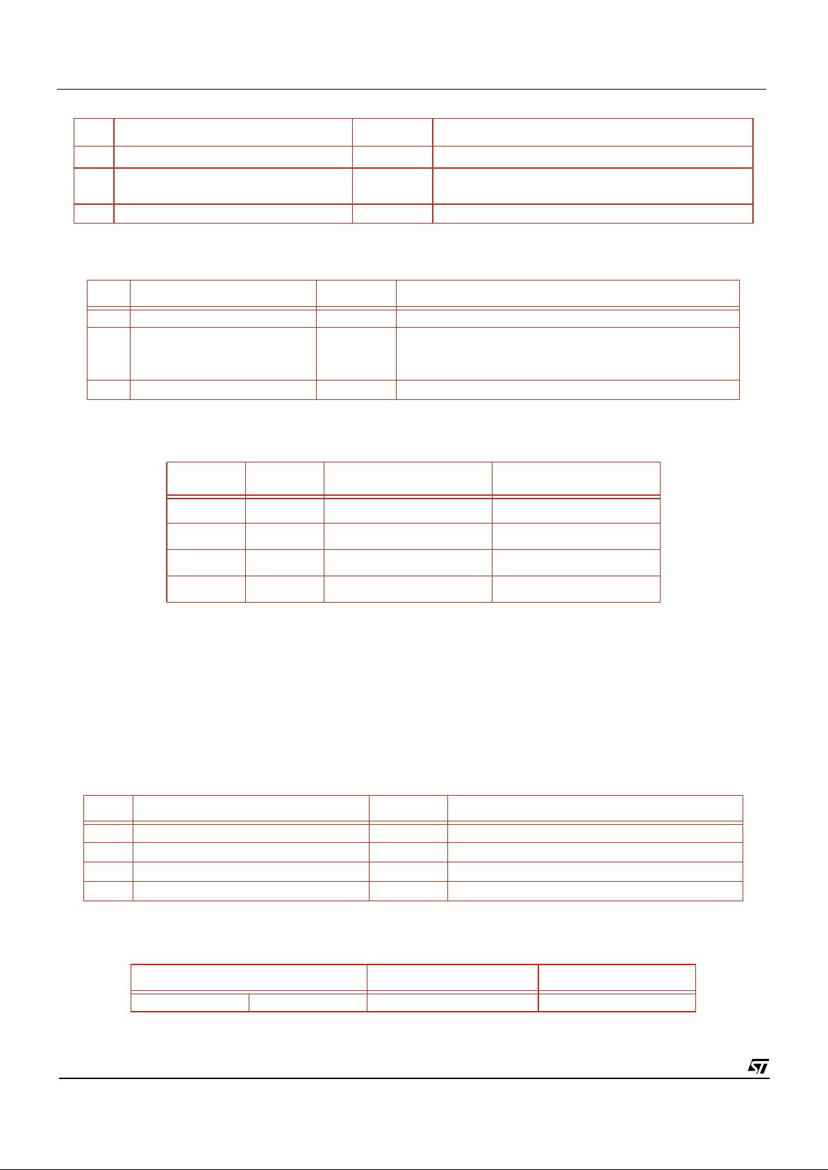
Setup 0 register controls some fundamental exposure and output format parameters. Defaults are shown in bold type.
[17],
[11]
- Setup1
Setup 1 register controls registers that are less likely to be modified on a regular basis. The user should note that the border
pixels/lines can be disabled/enabled independently from the enabling/disabling of the custom analogue horizontal shift register.
Bits Function Default Comment
7:0 Device type identifier 0001_0010
2
Most significant 8bits of 12bit code identifying the
chip type.
Table 11 : [1],
[1] -
DeviceH
Bit Function Default Comment
0 Exposure value update pending 0 New exposure setting sent but not yet consumed by the
exposure controller
1 Unused 0
2 Gain value update pending 0 New gain value sent but not yet consumed by the
exposure controller
7:4 Unused 0
Table 12 : [2],
[2]
- Status0
Bit Function Default Comment
0 Automatic exposure control.
Off/On
1 Enables or disables automatic exposure control.
Current exposure value is frozen when disabled.
1 Unused 1
2 Automatic gain control.
Off/On
1 Enables or disables automatic gain control. Current
gain value is frozen when disabled.
4:3 Unused 00
2
5 Data format select. 1 0 - 8 wire parallel output
1 - 4 wire parallel output
7:6 Unused 00
2
Table 13 : [16],
[10]
- Setup0
Bit Function Default Comment
0 Enable additional black lines (3-8)
Off/On
0 If enabled extra black lines are visible at device output
1 Unused 1
2 Enable horizontal shuffle mode.
Off/On
0 The contents of the horizontal shift register are shuffled
so that all the even columns then all the odd columns
are read out.
Table 14 : [17],
[11]
- Setup1
Page 32
VV5301 & VV6301 Serial Control Bus
cd5301_6301f-3-0.fm
Commercial in confidence
32/50
[19],
[13]
- Setup3
[20],
[14]
- Setup4
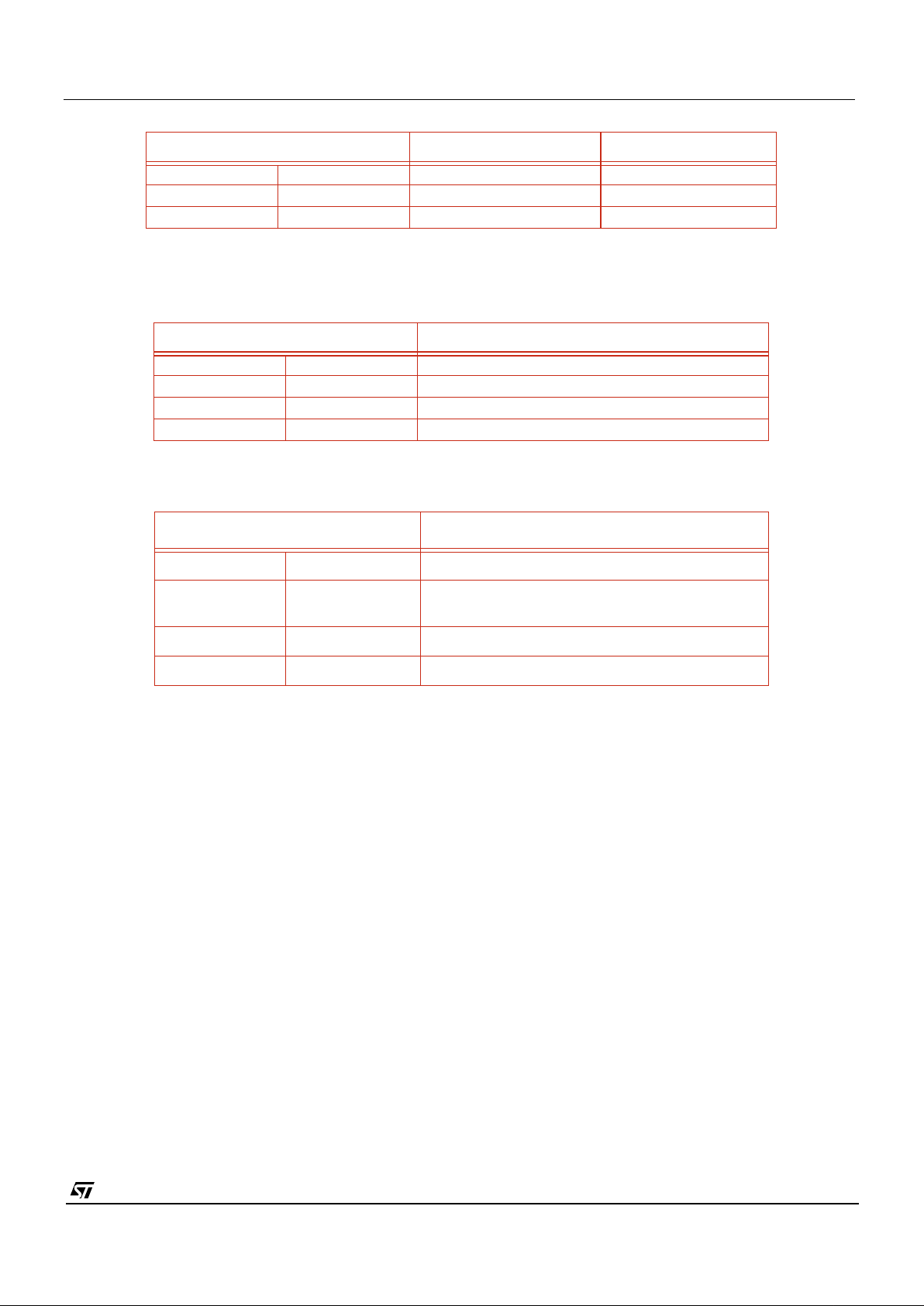
The data output on the serial wire or the 4/8 wire busses can be qualified by an internally generated clock signal, QCK. The QCK
function is assigned a dedicated pin, however the FST pin can also output QCK data, if reconfigured. By default, QCK is disabled.
The QCK can free run, qualify the embedded coding sequences and the visible data or the visible data only. FST can also be
enabled or disabled, default, or alternatively the FST pin can output a timing signal to synchronise several VV5301/VV6301
sensors or finally the FST pin can output the state of the custom analogue block successive approximation ADC output
comparator
5:3 Unused 110
2
6 50Hz timing/60Hz timing 1 The sensor will produce field rates either suited to
50Hz or 60Hz (default) operating environments.
7 Unused 0
Bit Function Default Comment
4:0 unused
6:5 Exposure step size 01 Selects exposure step size. 1/8 for fast but jerky
convergence to 1/64 for slow but smooth convergence.
Default 1/16. See Table 16 for details
7 Unused 0
Table 15 : [19],
[13]
- Setup3
Bit 6 Bit 5 Step size Comment
0 0 1/8
0 1 1/16 Default
1 0 1/32
1 1 1/64
Table 16 : Exposure step size options
Bit Function Default Comment
1:0 FST/QCK pin modes 00 See Table 18 below for details
3:2 QCK modes 00 See Table 19 below for details
5:4 unused
7:6 FST modes 00 See Table 20 below for details
Table 17 : [20],
[14]
- fg_modes
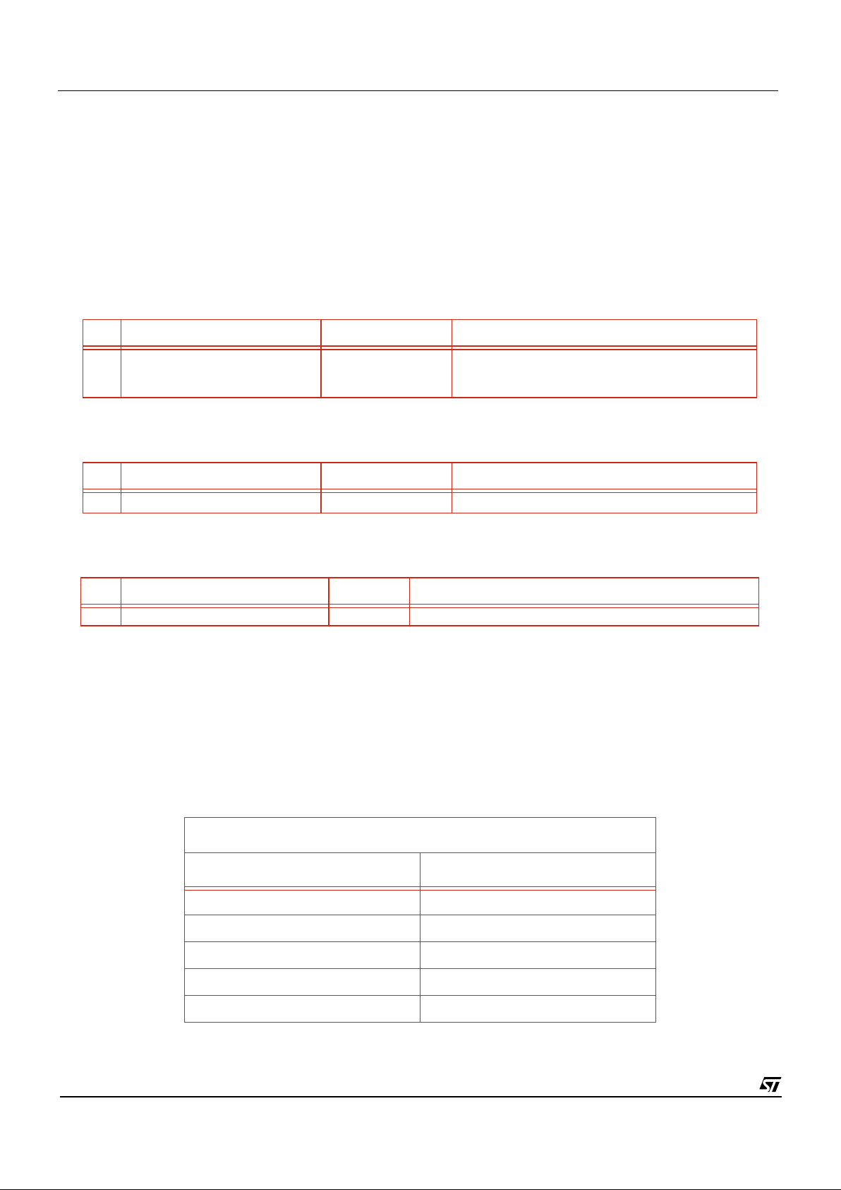
fg_mode[1:0] FST pin QCK pin
0 0 FST QCK
Table 18 : FST/QCK Pin Selection
Bit Function Default Comment
Table 14 : [17],
[11]
- Setup1
Page 33
CMOS Sensor; Customer Datasheet, Rev 3.0, 25 September 2000 VV5301 & VV6301
33/50
cd5301_6301f-3-0.fm
Commercial in confidence
note: The FST pin will always output the free running version of QCK (either inverted or normal)
.
[21-31],
[15-1F]
- unused
8.5.3 Exposure Control Registers [32 - 47],
[20-2F]
There is a set of parameters that control the time that the sensor pixels are exposed. The parameters are as follows: fine and
coarse exposure time, clock division control and finally gain control. The latter parameter does not affect the integration period
rather it amplifies the video signal at the output stage of the sensor core. An internal automatic algorithm will, if enabled,
continually monitor the pixel output and then, if required, use this data to correct the current exposure.
Manually changing the divisor applied to the incoming crystal clock can alter the effective integration of the sensor. By slowing the
internal clock down the integration period can be increased, i.e. halving the pixel clock frequency will double the integration
period.
If the user wishes to use the automatic exposure algorithm, the automatic exposure control (controlling
fine
and
coarse
exposure)
must be enabled. Additional gain control is optional. It is also possible to change the gain manually via the serial interface even if
the exposure is adjusted automatically.
If a user wishes to write an external value to one of the automatic exposure algorithm registers then it is advised that the
automatic control for that register be disabled prior to using the serial interface to write the external value.
Note:
The external exposure (coarse, fine or gain) values do not take effect immediately. Data from the serial interface is read by
the exposure algorithm at the start of a video frame. If the user reads an exposure value via the serial interface then the value
reported will be the data as yet unconsumed by the exposure algorithm, because the serial interface logic locally stores all the
data written to the sensor.
Between writing the exposure data and the point at which the data is consumed by the exposure algorithm, bit 0 of the status
register is set. The gain value is updated a frame later than the coarse and fine exposure parameters. The gain is applied directly
0 1 FST QCK
1 0 QCK
note
QCK
1 1 Invert QCK
note
QCK
fg_mode[3:2] QCK state
0 0 Off
0 1 Free Running
1 0 Valid during data and control period of line
1 1 Valid only during data period of line
Table 19 : QCK Modes
fg_mode[7:6]] FST pin
0 0 Off
0 1 Normal behaviour,FST will qualify the visible pixels in
the status line
1 0 Synchronisation out pulse, SNO
1 1 Output ADC comparator output, CPO
Table 20 : FST Modes
fg_mode[1:0] FST pin QCK pin
Table 18 : FST/QCK Pin Selection
Page 34
VV5301 & VV6301 Serial Control Bus
cd5301_6301f-3-0.fm
Commercial in confidence
34/50
at the video output stage and does not require the long set up time of the coarse and fine exposure settings.
The automatic exposure algorithm uses a set of exposure threshold settings. These thresholds may also be modified by the user
to alter the algorithm’s performance. The exposure algorithm uses these thresholds in a histogram. The three thresholds divide
the histogram into 4 regions, very overexposed, overexposed, underexposed and very underexposed. The pixel data received
from the sensor core is compared against the thresholds to determine the accuracy of the current exposure setting. A series of
flags are set to describe the outcome of the histogram comparison and the new exposure setting can then be derived.
Each exposure parameter is subject to a maximum setting. The fine exposure setting can be clamped to a fixed value regardless
of the decision made by the automatic algorithm. The clamping will occur if the coarse exposure setting exceeds a predetermined
value and the clamping has been enabled via the serial interface.
All 8 binary codes can be written to the core via the serial interface. Only the 4 thermometer codes 000,001,011 and 111 are
selected by the automatic exposure algorithm. The 4 other codes are however still valid and will be evaluated as detailed in the
table below. It is clear, from the non-linear relationship between the binary code and the actual gain applied at the analogue
output stage, that care should be taken when using non thermometer code gain settings. If the user writes a gain code of 110
(real gain = 1.600) and then enables automatic gain control and the controller then decided to reduce the gain, the new gain
value would be 011 (real gain = 4.000) i.e. the effective applied gain at the analogue output stage has actually been increased.
Care must be taken when writing manual gain values.
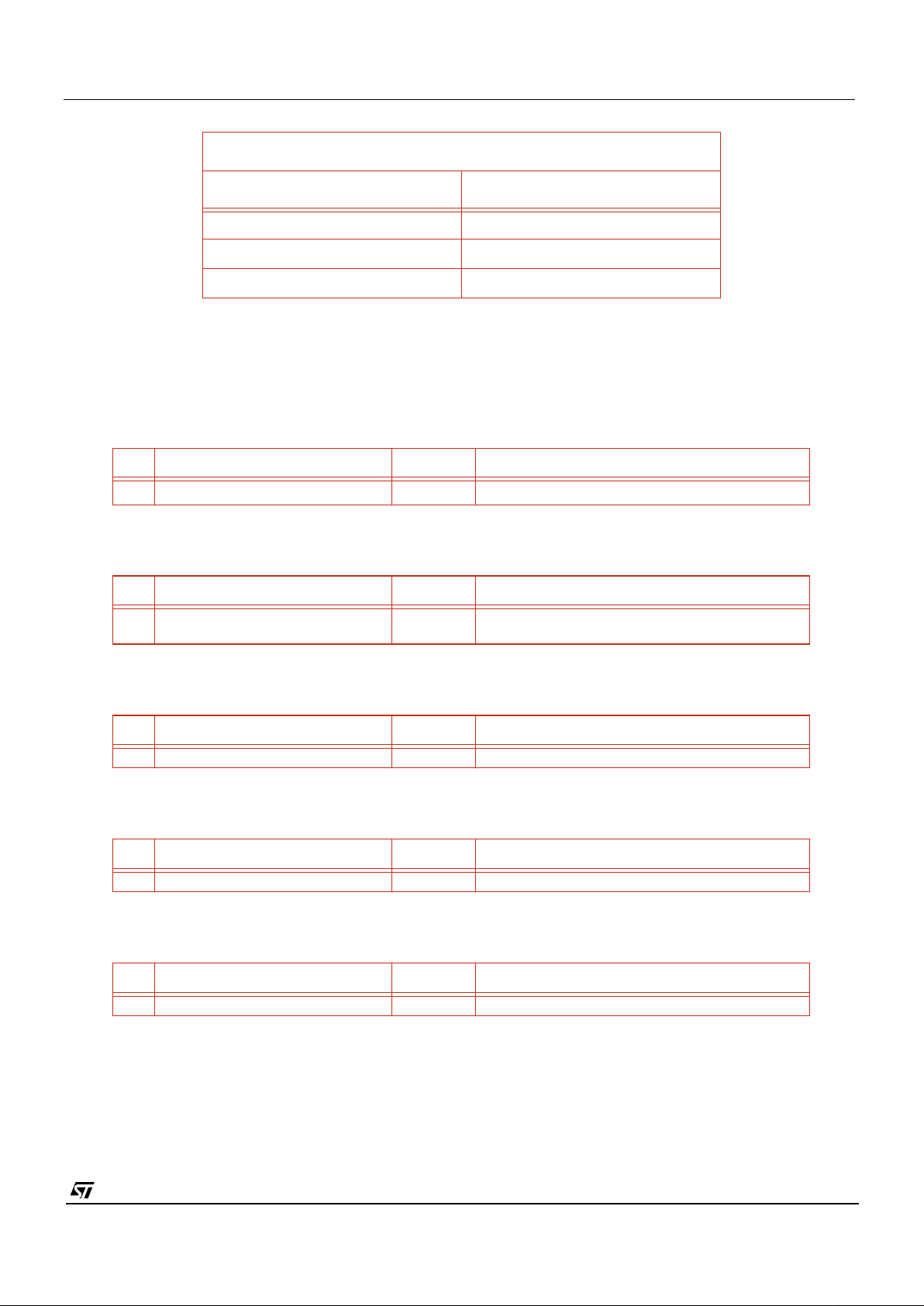
The effective system gain for a given binary gain code is as follows:
Bit Function Default Comment
7:0 Fine exposure value 0000_00002 (00H) maximum fine (50Hz mode) = FF
H
maximum fine (60Hz mode) = A8
H
Table 21 : [33],
[21]
- Fine Exposure Value
Bit Function Default Comment
7:0 Coarse exposure value 0111_00002 (70H) maximum coarse (50Hz and 60Hz modes) = 91
H
Table 22 : [34],
[22]
- Coarse Exposure Value
Bit Function Default Comment
2:0 Gain value 0 8 possible gain states can be written via the serial interface
Table 23 : [36],
[24]
- Gain Value
VV5301/6301
Gain binary code Effective system gain
000 1.000
001 2.000
010 1.333
011 4.000
100 1.143
Table 24 : System Gain
Page 35
CMOS Sensor; Customer Datasheet, Rev 3.0, 25 September 2000 VV5301 & VV6301
35/50
cd5301_6301f-3-0.fm
Commercial in confidence
The
undivided
input crystal clock is used by the clock generator circuitry, elements of the serial interface and a small number of
other registers in the design. The remaining digital logic and the analogue circuitry, use internally generated clocks, namely the
pixel clock and the faster ADC clocks. These clocks are all slower versions of the crystal clock. The ADC clocks may be up to half
the crystal frequency, but can be further divided by factors of 2, 4 or 8. The pixel clock is lower frequency than the ADC clock.
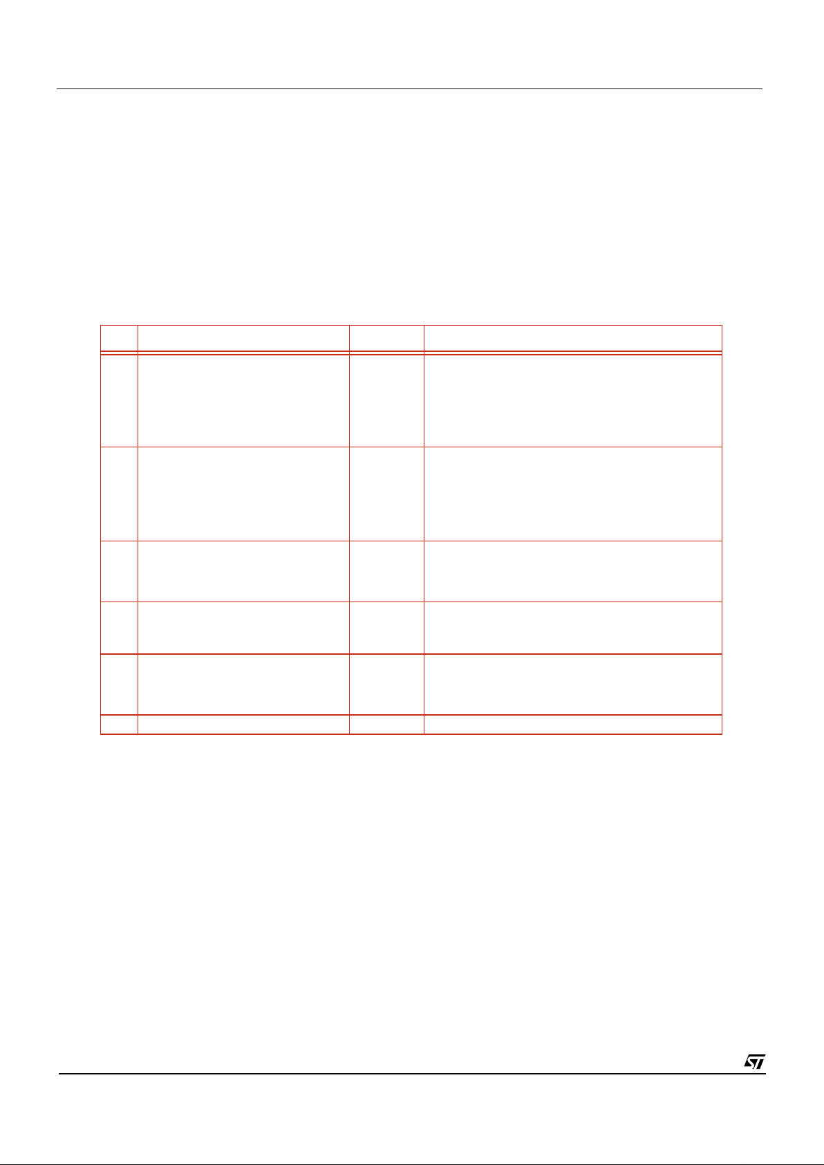
101 2.667
110 1.600
111 8.000
Bit Function Default Comment
1:0 Clock divisor value 0
Pixel clock = Crystal clock ÷2
n+1
Table 25 : [37],
[25]
- Clock Divisor Value
Bit Function Default Comment
2:0 Gain limit 7 The programmed gain cannot be greater than this
value
Table 26 : [38],
[26]
- Gain Limit
Bit Function Default Comment
7:0 Exposure lower threshold 85
Table 27 : [39],
[27]
- Exposure Lower Threshold
Bit Function Default Comment
7:0 Exposure centre threshold 100
Table 28 : [40],
[28]
- Exposure Centre Threshold
Bit Function Default Comment
7:0 Exposure higher threshold 115
Table 29 : [41],
[29]
- Exposure Higher Threshold
VV5301/6301
Gain binary code Effective system gain
Table 24 : System Gain
Page 36
VV5301 & VV6301 Serial Control Bus
cd5301_6301f-3-0.fm
Commercial in confidence
36/50
[41-47],
[29-2F]
- unused
[48-111],
[30-6F]
- reserved
8.5.4 System Registers [112-127],
[70-7F]
[112],
[70]
- Black Calibration Setup Register
The sensor contains an automatic function to help maintain an ideal black level for the video signal. The centre 128 pixels, from
the designated black lines are summed, averaged and then compared with a reference, to determine if the black level has to be
adjusted. If an adjustment is required then the values of the 2 DAC registers, B0 and B1 - addresses [113-114],
[71-72]
, can be
altered to remove any offset in the video black level.
It is strongly recommended that the user select 2’b01 for bits[1:0] of register[112],
[70].
This will ensure that the black calibration
algorithm will run each field.
The monitor window size is programmable. If bit 4 of the register above is set then bits[3:2] will determine the size of the monitor
window otherwise the current gain setting will fix the monitor window width.
There are two DAC value adjustment phases during black calibration. The first is a successive approximation technique to
establish an
approximate
value for the DAC register. This estimate is then improved by a linear tracking routine. The latter will
change the DAC register setting if the current pixel average is outwith the black calibration target window. The target window can
also be altered via the serial interface.
It will only be possible to read back the values of the DAC registers, as set by the automatic black cal algorithm, with the VV5301/
VV6301 sensors.
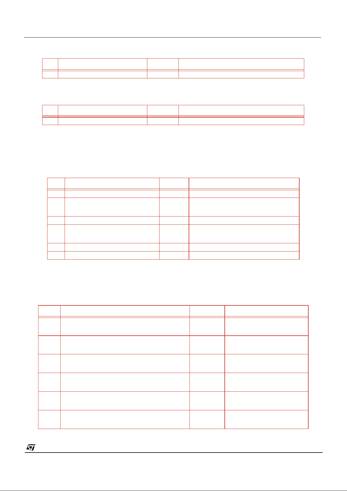
Bit Function Default Comment
1:0 Black calibration trigger select 101 00 - Never BCal
01 - Always BCal
10 - BCal if failed monitor
11 - BCal if gain has changed
3:2 Black calibration monitor window
select (pixel average comparison
range)
00 00 - 14.00 to 17.99
01 - 13.00 to 18.99
10 - 12.00 to 19.99
11 - 11.00 to 20.99
4 Monitor window size set by serial
interface.
Yes/No
0 If enabled the monitor window size is set directly by
the user via the serial interface
5 Narrow bcal target window
Yes/No
0 If enabled the bcal test target window can be
narrowed to force pixel black level closer to the
ideal 16.00 value.
6 External black calibration DAC
register values
Yes/No
0 If enabled the DAC values used by the analogue
sensor core
7 unused 0
Table 30 : [112],
[70] -
Black Calibration Window Parameters
Page 37
CMOS Sensor; Customer Datasheet, Rev 3.0, 25 September 2000 VV5301 & VV6301
37/50
cd5301_6301f-3-0.fm
Commercial in confidence
[116],
[74] -
System Test
The sensor can operate in several different test modes. These test modes detect faults in the sensor pixel array and the
supporting analogue circuitry. Only one test mode should be enabled at any time.
‘[118-119],
[76-77]
- Analogue Control Registers
There are 2 registers used to configure the custom analogue section of the sensor.
Bit Function Default Comment
7:0 bcal0 80H This register is read only
Table 31 : [113],
[71]
- Black Calibration DAC B0
Bit Function Default Comment
7:0 bcal1 80H This register is read only
Table 32 : [114],
[72]
- Black Calibration DAC B0
Bit Function Default Comment
0 reserved 0
1 Tristate digital outputs
Yes/No
0 If enabled the upper nibble of the data bus,
FST & QCK will be tristated.
2 reserved 0
3 Tristate digital outputs
Yes/No
0 If enabled the lower nibble of the data bus
will be tristated.
6:4 reserved
7 unused
Table 33 : [116]
,[74]
- System Test
Bit Function Default Comment
0 Enable bit line clamp
Off/On
0
1 Inhibit horizontal shift register
Off/On
0
2 Enable anti-blooming protection
Off/On
0
3 Inhibit OSA fast reset
Off/On
0
4 External bit line white reference
Off/On
0
5 Inhibit array read during blank lines
Off/On
0 Disable additional MFI and
BLOOP signals
Table 34 : [118],
[76]
- Analogue Control Register 0
Page 38
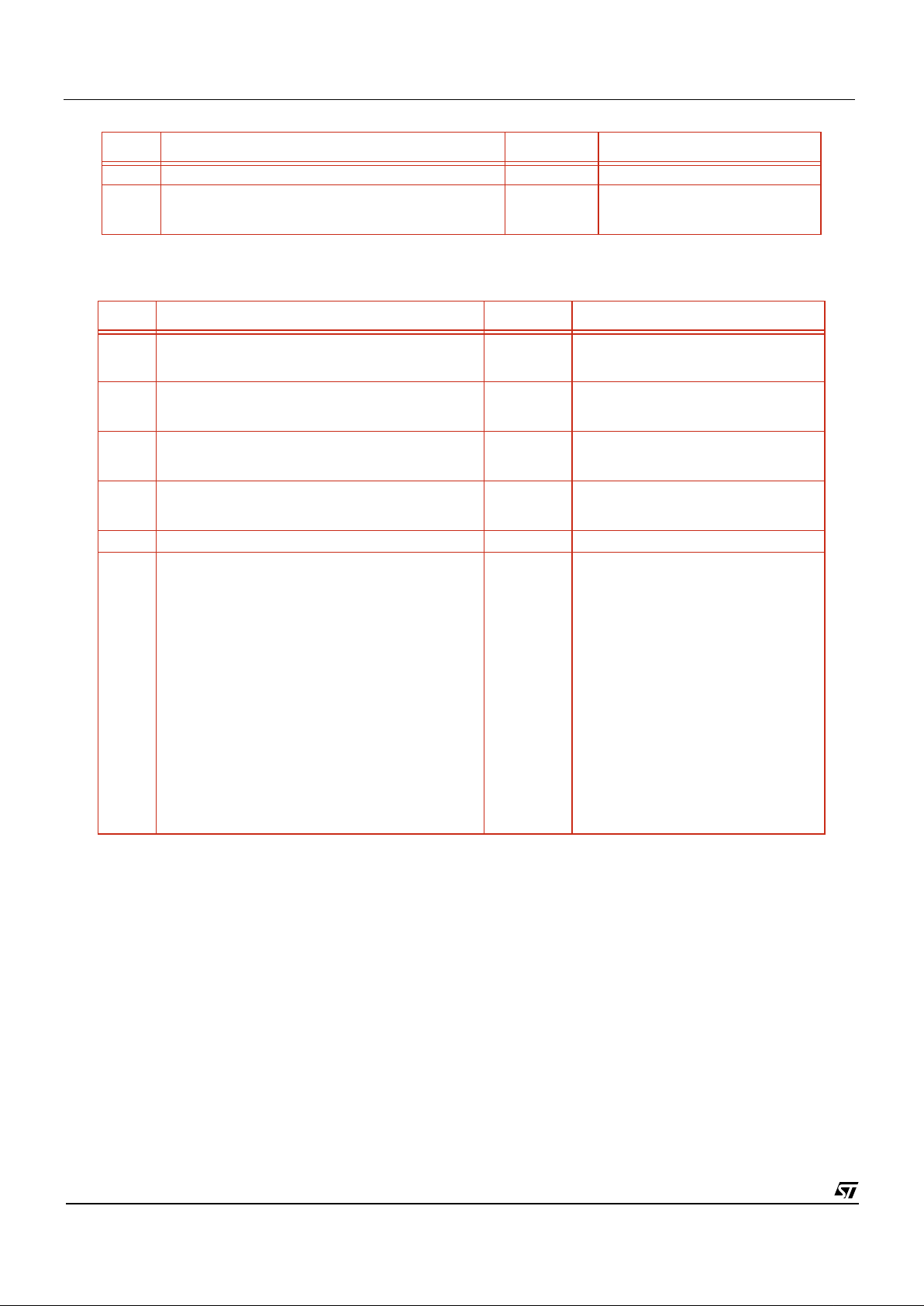
VV5301 & VV6301 Serial Control Bus
cd5301_6301f-3-0.fm
Commercial in confidence
38/50
6 unused 0
7 RST/MRST clock select 0 0 - adck0
1 - adck1
Bit Function Default Comment
0 Enable Mag_B0
Off/On
0 Double magnitude of B0 DAC current
1 New PXRDB scheme
Off/On
0
2 B1 Offset DAC High Gain Select
low (x1)/High (x2)
0 B1_HG
3 Stand-by
Off/On
0 Powers down ALL analogue circuitry
and the majority of the digital logic
4 unused 0
7:5 RST/MRST phase select 000 The RST/MRST timing signals can be
delayed by up to 7 adck periods prior
to transfer to the analogue circuits.
000 - no delay
001 - 1 adck period delay
010 - 2 adck period delay
011 - 3 adck period delay
100 - 4 adck period delay
101 - 5 adck period delay
110 - 6 adck period delay
111 - 7 adck period delay
Table 35 : [119]
,[77]
- Analogue Control Register1
Bit Function Default Comment
Table 34 : [118],
[76]
- Analogue Control Register 0
Page 39
CMOS Sensor; Customer Datasheet, Rev 3.0, 25 September 2000 VV5301 & VV6301
39/50
cd5301_6301f-3-0.fm
Commercial in confidence
8.6 Types of messages
This section gives guidelines on the basic operations to read data from and write data to the serial interface.
The serial interface supports variable length messages. A message may contain no data bytes, one data byte or many data
bytes. This data can be written to or read from common or different locations within the sensor. The range of instructions
available are detailed below.
• Write no data byte, only sets the index for a subsequent read message.
• Single location data write or read for monitoring (real time control)
• Multiple location read or write for fast information transfers.
Examples of these operations are given below. A full description of the internal registers is given in the previous section. For all
examples the slave address used is 32
10
for writing and 3310 for reading. The write address includes the read/write bit (the lsb)
set to zero while this bit is set in the read address.
8.6.1 Single location, single data write.
When a random value is written to the sensor, the message will look like this:
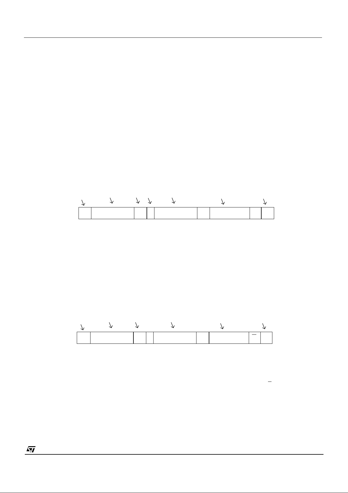
In this example, the
fineH
exposure register (index = 3210) is set to 8510. The r/w bit is set to zero for writing and the
inc
bit (msbit
of the index byte) is set to zero to disable automatic increment of the index after writing the value. The address index is preserved
and may be used by a subsequent read. The write message is terminated with a stop condition from the master.
8.6.2 Single location, single data read.
A read message always contains the index used to get the first byte.
This example assumes that a write message has already taken place and the residual index value is 32
10
. A value of 8510is read
from the
fineH
exposure register. Note that the read message is terminated with a negative acknowledge (A) from the master: it is
not guaranteed that the master will be able to issue a stop condition at any other time during a read message. This is because if
the data sent by the slave is all zeros, the
sda
line cannot rise, which is part of the stop condition.
8.6.3 No data write followed by same location read.
When a location is to be read, but the value of the stored index is not known, a write message with no data byte must be written
first, specifying the index. The read message then completes the message sequence. To avoid relinquishing the serial to bus to
another master a repeated start condition is asserted between the write and read messages, i.e. no stop condition is asserted. In
Figure 15 : Single location, single write.
S 3210A0 32
10
A8510A P
Start
Device
Ack
address
Index Data
Stop
Inc
Figure 16 : Single location, single read.
S 3310A0 32
10
A8510A P
Start
Device
Ack
address
Index Data
Stop
Page 40
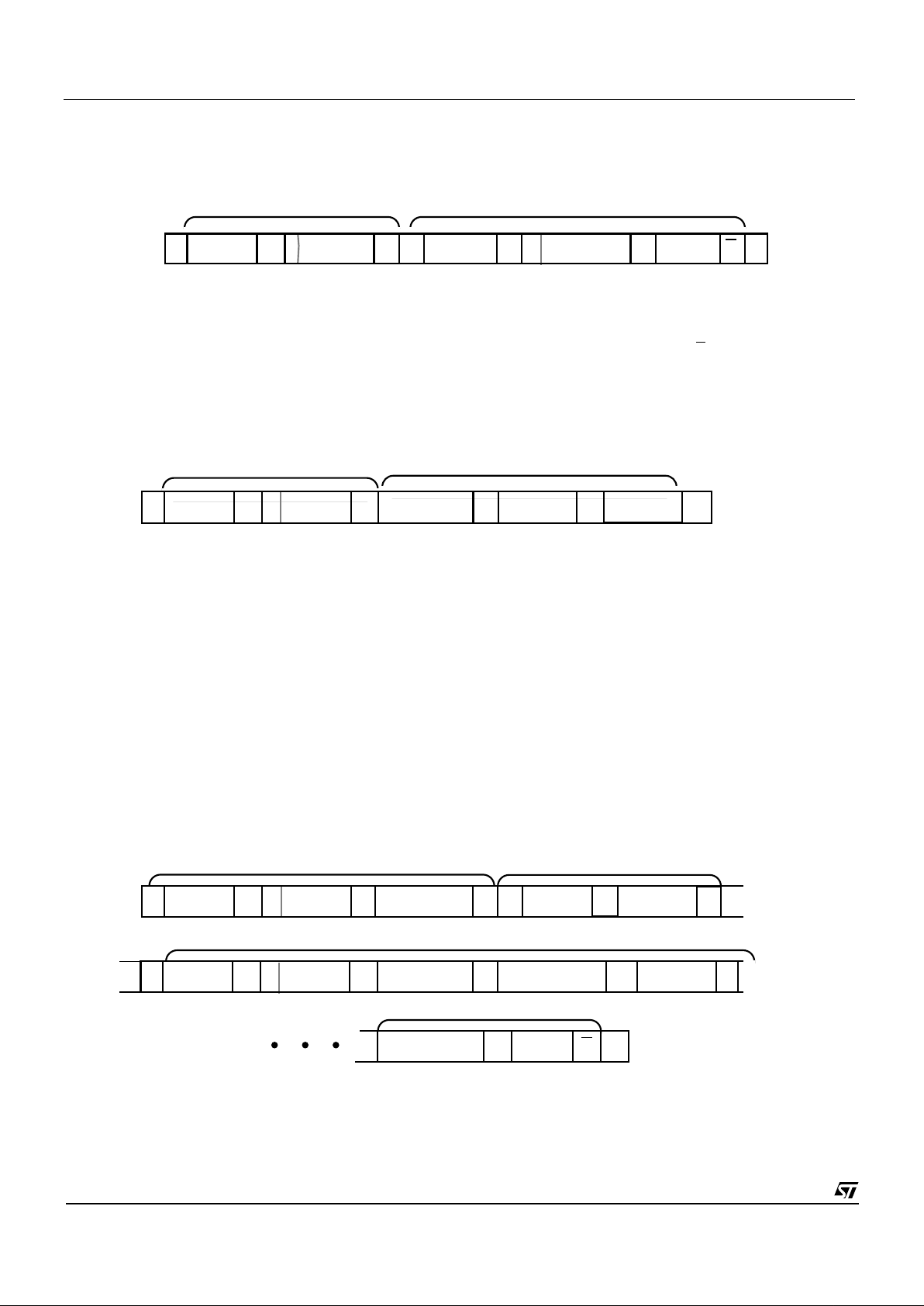
VV5301 & VV6301 Serial Control Bus
cd5301_6301f-3-0.fm
Commercial in confidence
40/50
this example, the
gain
value (index = 3610) is read as 1510:
As mentioned in the previous example, the read message is terminated with a negative acknowledge (
A) from the master.
8.6.4 Same location multiple data write.
It may be desirable to write a succession of data to a common location. This is useful when the status of a bit must be toggled.
8.6.5 Same location multiple data read
When an exposure related value (
fine
H, fineL, coarseH, coarse L
,
gain or clk_div
) is written, it takes effect on the output at the beginning of the next video frame,
(remember that the application of the
gain
value is a frame later than the other exposure parameters). To signal the consumption
of the written value, a flag is set when any of the exposure or gain registers are written and is reset at the start of the next frame.
This flag appears in
status0
register and may be monitored by the bus master. To speed up reading from this location, the sensor
will repeatedly transmit the current value of the register, as long as the master acknowledges each byte read.
In the below example, a
fineH
exposure value of 0 is written, the status register is addressed (no data byte) and then constantly
read until the master terminates the read message.
Figure 17 : No data write followed by same location read.
S
A
Sr A
A
A
P
33
10
36
10
33
10
36
10
1510A
0
0
No data write Read index and data
SA A
A
32
10
21
10
4
10
0
10
A
0
Write to
pin_mapping
Figure 18 : Same location multiple data write.
4
10
P
Toggle control bit
SA 0
10
AA A32
10
33
10
32
10
0
10
A0
Sr A AA A33
10
0
10
1
10
1
10
1
10
A0
Sr
Write
fineL
with zero Address the status0 register
A
1
10
010A
Read continuously...
...until flag reset
P
Figure 19 : Same location multiple data read.
Page 41
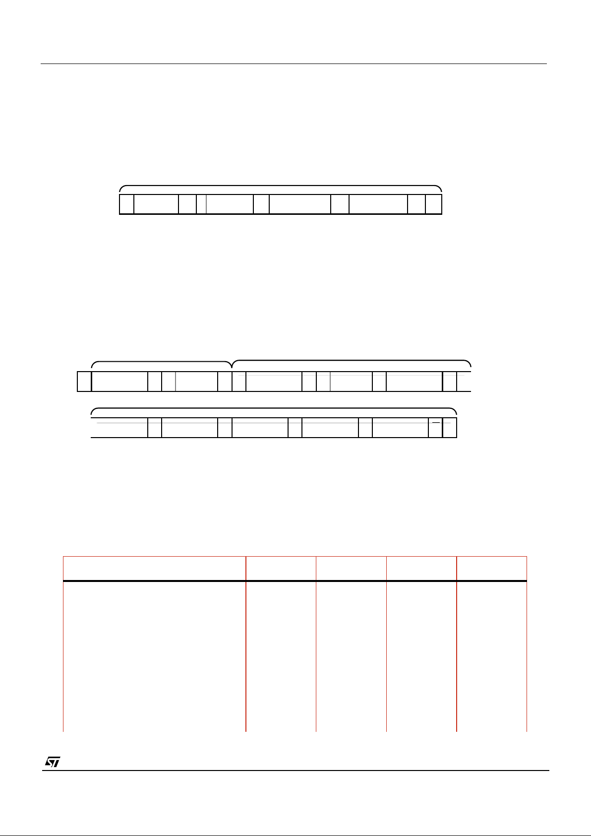
CMOS Sensor; Customer Datasheet, Rev 3.0, 25 September 2000 VV5301 & VV6301
41/50
cd5301_6301f-3-0.fm
Commercial in confidence
8.6.6 Multiple location write
If the automatic increment bit is set (msb of the index byte), then it is possible to write data bytes to consecutive adjacent internal
registers, (i.e. 23,24,25,26 etc), without having to send explicit indexes prior to sending each data byte. An auto-increment write to
the exposure registers with their default values is shown in the following example, where we write 17
10
to the pin_mapping
register[21] and 193
10
to the data format register[22].
.
8.6.7 Multiple location read
In the same manner, multiple locations can be read with a single read message. In this example the index is written first, to
ensure the exposure related registers are addressed and then they are read. Note that the user will get the base index, in this
case 32
10
, read back
twice
before the first data byte is read back. The user must therefore always request an extra byte of data
to be read back.
Note that a stop condition is not required after the final negative acknowledge from the master, the sensor will terminate the
communication upon receipt of the negative acknowledge from the master.
8.7 Serial Interface Timing
Parameter Symbol Min. Max. Unit
SCL clock frequency fscl 0 100 kHz
Bus free time between a
stop
and a
start
tbuf 2 - us
Hold time for a repeated
start
thd;sta 80 - ns
LOW period of SCL tlow 320 - ns
HIGH period of SCL thigh 160 - ns
Set-up time for a repeated
start
tsu;sta 80 - ns
Data hold time thd;dat 0 - ns
Data Set-up time tsu;dat 0 - ns
Table 36 : Serial Interface Timing Characteristics
SA 17
10
AAA32
10
21
10
193
10
1
Incremental write
P
Figure 20 : Multiple location write.
Incremental read
SAA32
10
32
10
1 Sr 33
10
AA32
10
1
32
10
A
AP
fineH
fineL
coarseH
coarseL
gain
AAAA
No data write
Incremental read
Figure 21 : Multiple location read.
Page 42
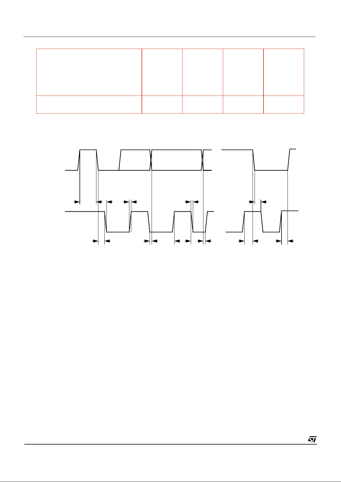
VV5301 & VV6301 Serial Control Bus
cd5301_6301f-3-0.fm
Commercial in confidence
42/50
Rise time of SCL, SDA tr - 300 ns
Fall time of SCL, SDA tf - 300 ns
Set-up time for a
stop
tsu;sto 80 - ns
Capacitive load of each bus line (SCL,
SDA)
Cb - 200 pF
Parameter Symbol Min. Max. Unit
Table 36 : Serial Interface Timing Characteristics
SDA
SCL
thd;sta
tr
thightftsu;datthd;dat tsu;sta tsu;sto
...
...
thd;statlowtbuf
stopstartstop start
all values referred to the minimum input level (high) = 3.5V, and maximum input level (low) = 1.5V
Figure 22 : Serial Interface Timing Characteristics
Page 43
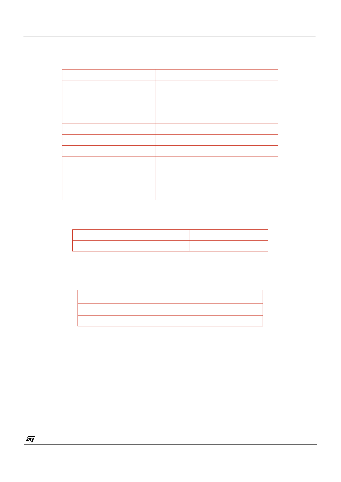
CMOS Sensor; Customer Datasheet, Rev 3.0, 25 September 2000 VV5301 & VV6301
43/50
cd5301_6301f-3-0.fm
Commercial in confidence
9. Detailed AC/DC Specification
9.1 VV5301/VV6301 AC/DC Specification
Table 37 : VV5301/VV6301 AC/DC specification
9.2 VV5301/VV6301 Power Consumption
Table 38 : VV5301/VV6301 Current consumption in different modes
9.3 Digital Input Pad Pull-up and Pull-down Resistors
Table 39 : VV5301/ 6301 pull up/pull down resistor specification
Image Format 160 x 120 pixels (QSIF)
Image size output 164 x 124 pixels
Pixel Size 12.5 x 12.5µm
Array Format QSIF
Exposure control up to 44000:1
Sensor signal / Noise ratio 36dB
Supply Voltage 5.0v +/-10%
Package type 48BGA
Operating Temp. range 0
o
C - 40oC
Logic 0 input 0.2 x Vdd Max
Logic 1 input 0.8 x Vdd Min
Serial interface frequency range 0-100kHz
Low power mode current consumption 4.6mA
Normal operating mode current consumption 15.1mA
Pad Type Pads Typical resistance
Library pulldown d[7:0],hpix,sin tba
Library pullup scl, sda, ce, qcktri tba
Page 44
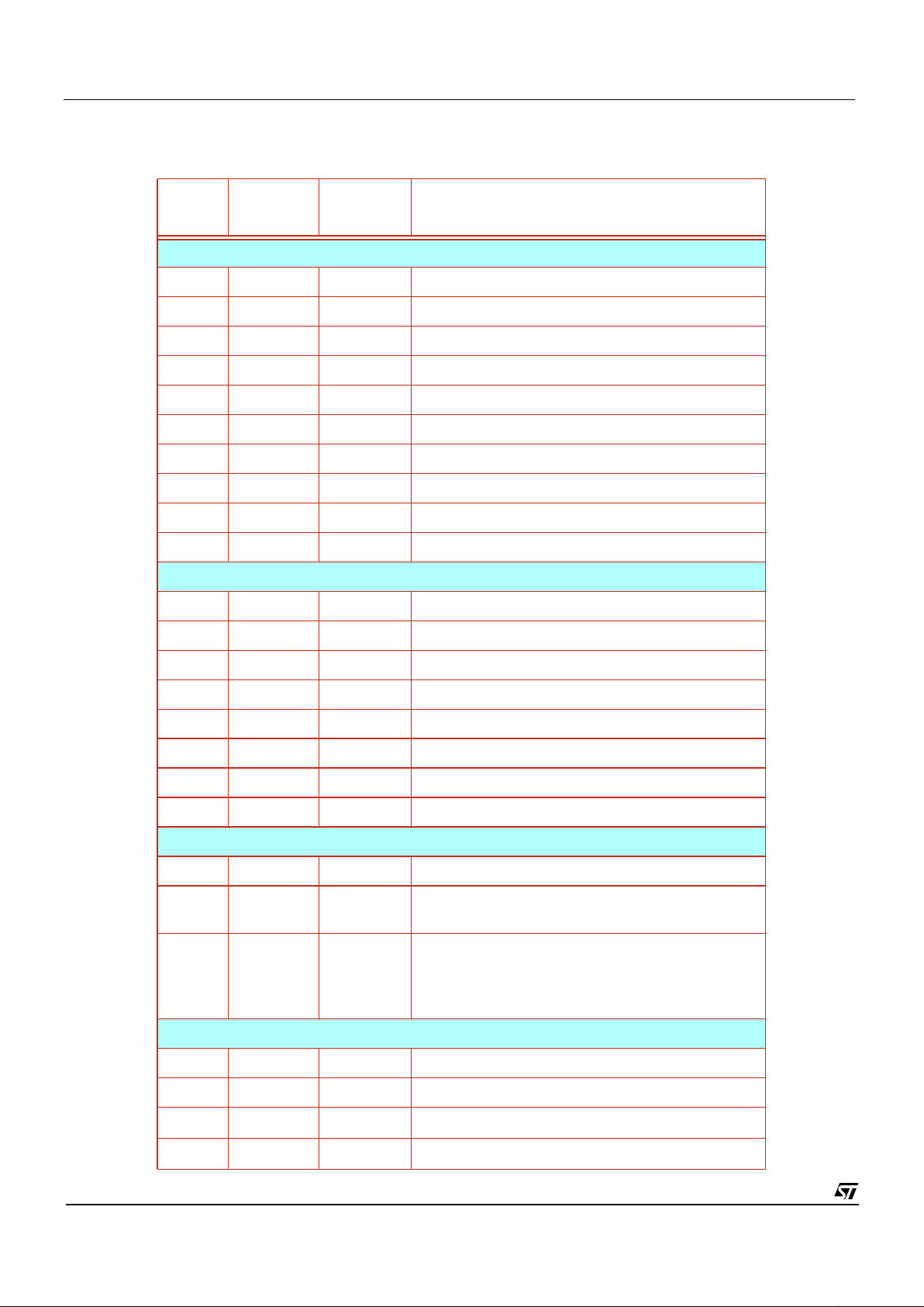
VV5301 & VV6301 Pinout and Pin Descriptions
cd5301_6301f-3-0.fm
Commercial in confidence
44/50
10. Pinout and Pin Descriptions
BGA
Pin
Name Type Description
POWER SUPPLIES
C5 AVSS GND Analogue ground
A7 AVDD PWR Analogue power
D7 DVDD PWR Digital power
D5 VDD PWR Power
G7 VDD PWR Power
F6 VSS GND Ground
G2 VSS GND Ground
F3 VDD PWR Power
E1 VSS GND Ground
E2 DVSS GND Ground
ANALOGUE OUTPUTS
B4 VRT IA Pixel reset voltage
A5 VCDS IA Voltage reference
B5 TEST IA Analogue test
C3 VREG OA Reference voltage input
B3 VBLOOM OA Internal reference voltage
A3 VBLTW IA Bitline test white reference
C4 VBG OA Internally generated bangap reference voltage 1.22V
A4 VREF2V5 OA Internally generated reference voltage 2.5V
DIGITAL OUTPUTS
E6 FST OD Frame start. Synchronises external image capture.
F7 QCK OD Pixel sample clock. Qualifies video output for external
image capture.
G6,E5,
G5,F5,
G4,F4,
G3,E4
D[7:0] OD↑ Parallel 8-wire databus.
VV5301/VV6301 only, bidirectional pads always
configured as outputs
DIGITAL CONTROL SIGNALS
E3 SCL BI↑ Serial bus clock (bidirectional, open drain)
F1 SDA BI↑ Serial bus data (bidirectional, open drain)
D1 QCKTRI ID↓
QCK tristate
D2 CE ID↑
Chip enable
Page 45
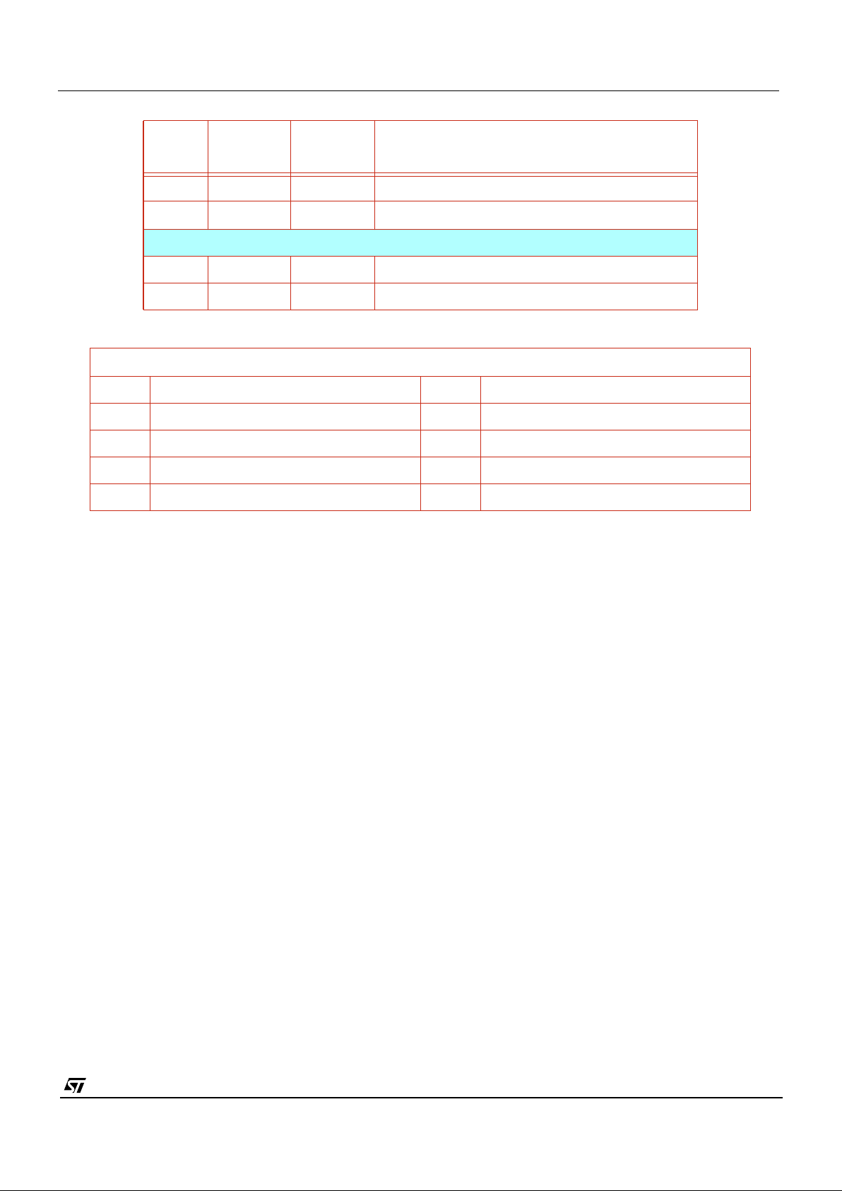
CMOS Sensor; Customer Datasheet, Rev 3.0, 25 September 2000 VV5301 & VV6301
45/50
cd5301_6301f-3-0.fm
Commercial in confidence
A6 HPIX ID↓ Hold pixel value.
E7 SIN ID↓
Sensor synchronisation
SYSTEM CLOCKS
G1 CLKI ID Oscillator input.
F2 CLKO OD Oscillator output.
Key
A Analog Input ΙD Digital Input
OA Analog Output ID↑ Digital input with internal pull-up
BI Bidirectional ID↓ Digital input with internal pull-down
BI↑ Bidirectional with internal pull-up OD Digital Output
BI↓ Bidirectional with internal pull-down ODT Tri-stateable Digital Output
BGA
Pin
Name Type Description
Page 46
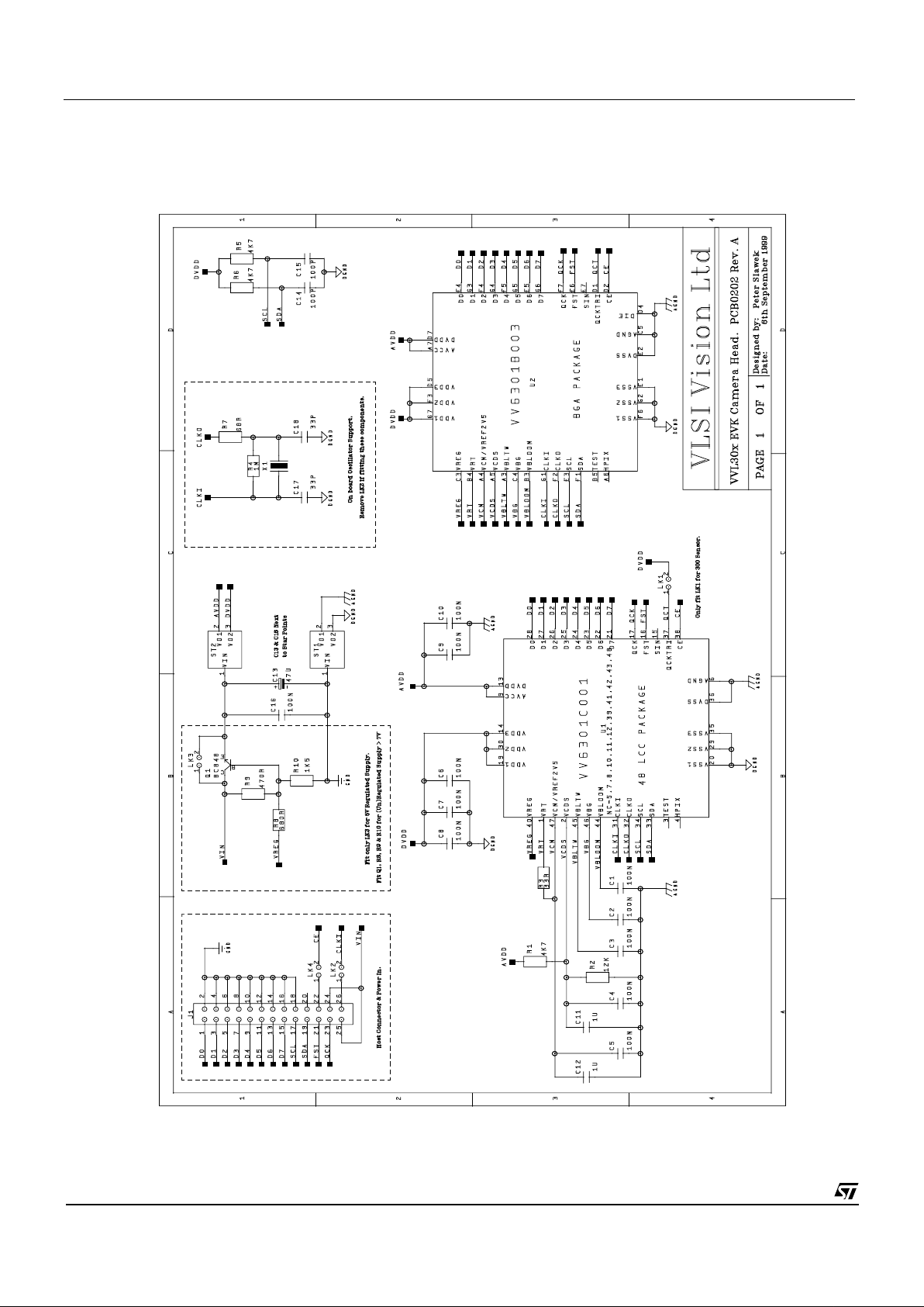
VV5301 & VV6301 VV5301/VV6301 Recommended Reference Design
cd5301_6301f-3-0.fm
Commercial in confidence
46/50
11. VV5301/VV6301 Recommended Reference Design
Page 47
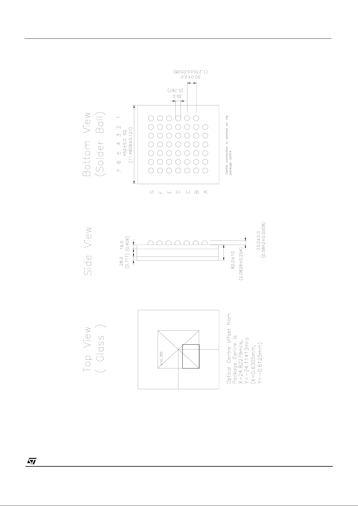
CMOS Sensor; Customer Datasheet, Rev 3.0, 25 September 2000 VV5301 & VV6301
47/50
cd5301_6301f-3-0.fm
Commercial in confidence
12. Package Details (48 pin BGA (VV5301/VV6301)
Figure 23 : Package drawing for 48pin BGA with VVx301
Page 48

VV5301 & VV6301 Evaluation kits (EVK’s)
cd5301_6301f-3-0.fm
Commercial in confidence
48/50
13. Evaluation kits (EVK’s)
It is highly recommended that an Evaluation Kit (EVK) is used for initial evaluation and design-in of the VV5301/VV6301. Please
contact STMicroelectronics for further details.
Page 49
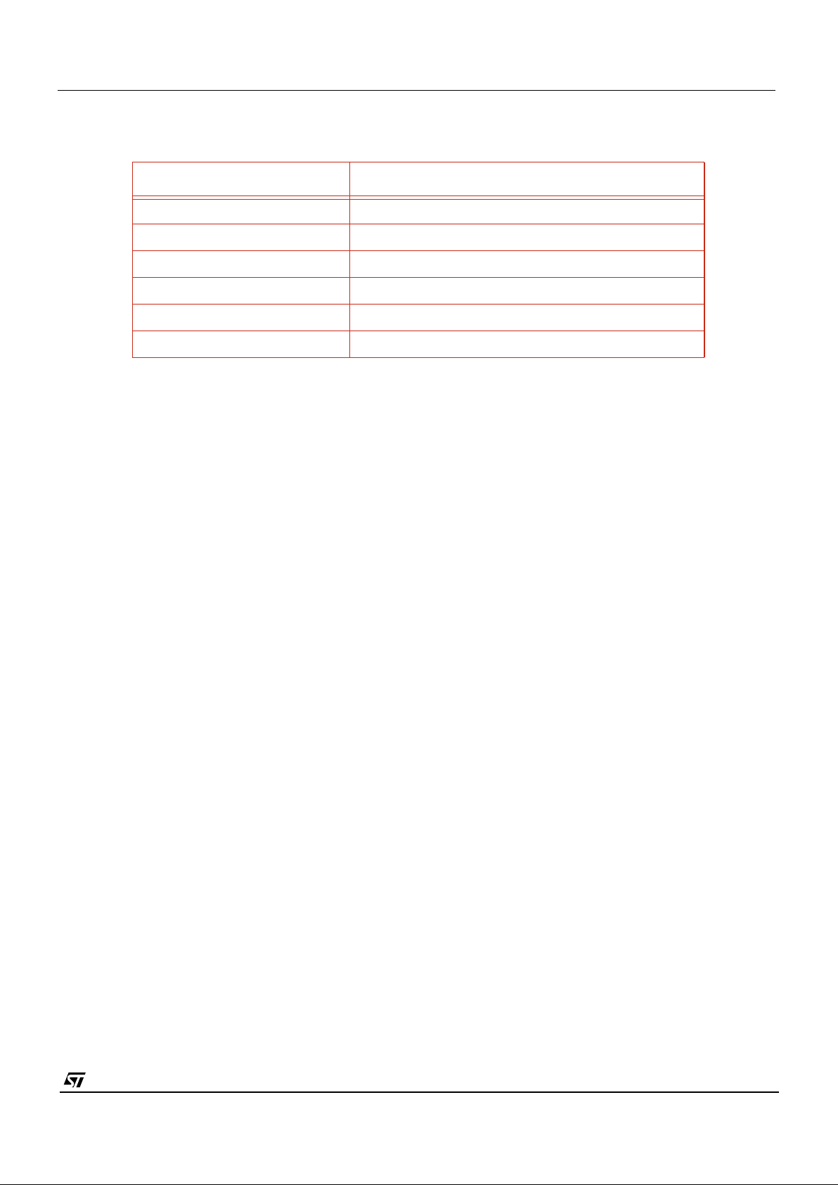
CMOS Sensor; Customer Datasheet, Rev 3.0, 25 September 2000 VV5301 & VV6301
49/50
cd5301_6301f-3-0.fm
Commercial in confidence
14. Ordering Details
Part Number Description
VV5301B001 BGA packaged, QSIF Monochrome sensor
VV6301B001 BGA packaged, QSIF Colour sensor
STV-5301-R01 Reference design board for (mono) 5301 sensor
STV-6301-R01 Reference design board for (colour) 6301 sensor
STV-5301-E01 Evaluation kit (monochrome)
STV-6301-E01 Evaluation kit (colour)
Page 50

VV5301 & VV6301 Ordering Details
cd5301_6301f-3-0.fm
Commercial in confidence
Information furnished is believed to be accurate and reliable. However, STMicroelectronics assumes no responsibility for the
consequences of use of such information nor for any infringement of patents or other rights of third parties which may result from
its use. No license is granted by implication or otherwise under any patent or patent rights of STMicroelectronics. Specifications
mentioned in this publication are subject to change without notice. This publication supersedes and replaces all information
previously supplied. STMicroelectronics products are not authorized for use as critical components in life support devices or
systems without express written approval of STMicroelectronics
The ST logo is a registered trademark of STMicroelectronics
© 2000 STMicroelectronics - All Rights Reserved
.Imaging Division
50/50
www.st.com
 Loading...