

Page 1
BUS CONTROLLEDPAL/NTSC TV PROCESSOR
.
I2C BUS CONTROL OF ALLFUNCTIONS
.
INTEGRATEDFILTERS(TRAP,BANDPASS)
.
INTEGRATEDLUMINANCEDELAYLINE
.
PAL/NTSCCHROMADEMODULATORS
.
NTSCAUTOMATIC FLESH TONECONTROL
.
AUTOMATICCUT-OFF CURRENTLOOP
.
TWORGB INPUTS
.
SVHSSWITCH
.
TWOPLLs HORIZONTAL DEFLECTION
.
VERTICALCOUNT DOWN
.
3 CRYSTALSAPPLICATIONCAPABILITY
.
BLUESCREEN
.
VERYFEW EXTERNALCOMPONENTS
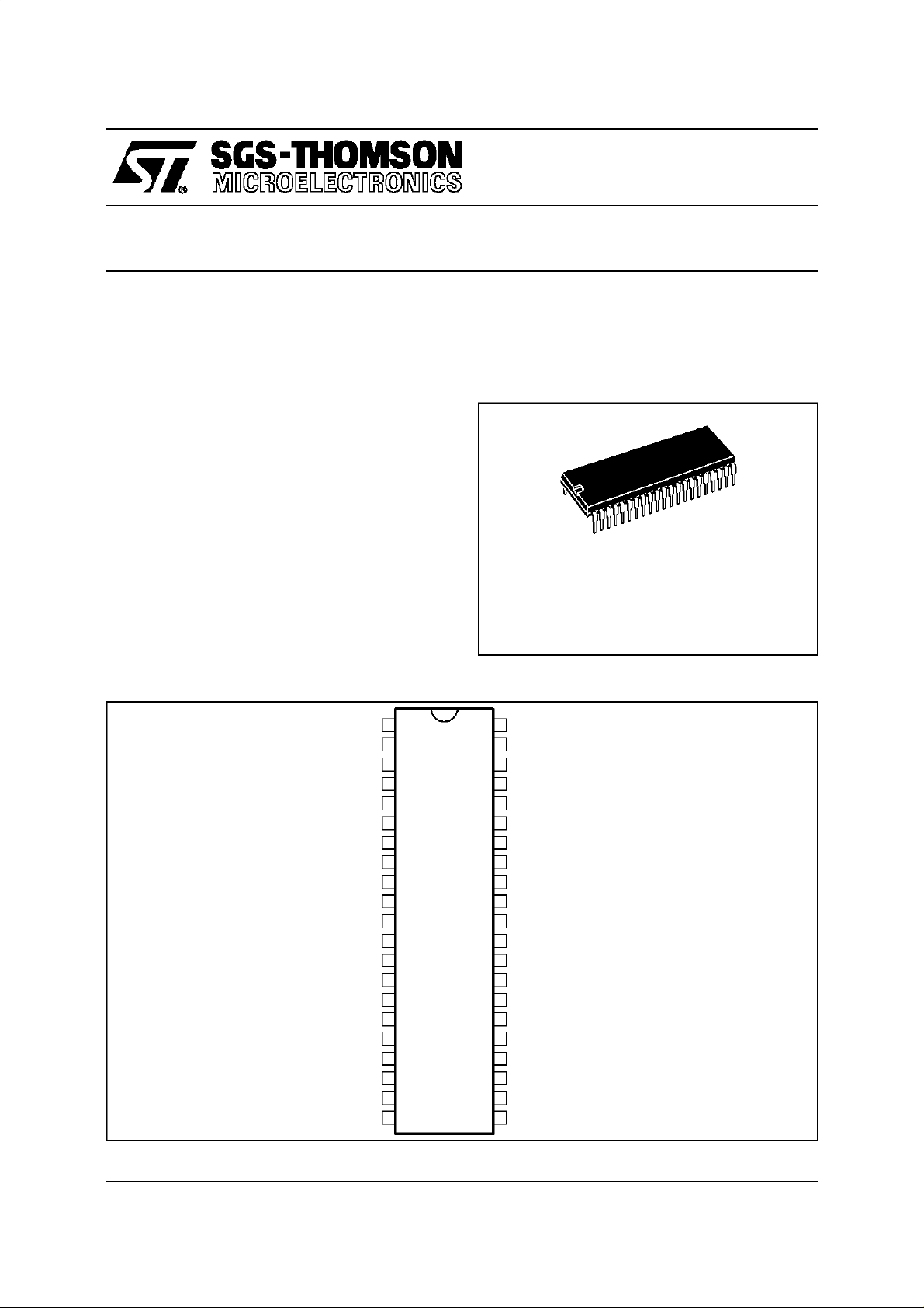
STV2116A
Used withSTV8223(PIF/SIF/switches),TDA1771
or TDA8174 (frame booster), STV2180 (delay
line), it allows to design a PAL/NTSC (BGDKIMN)
set with very few external components and no
adjustment.
SHRINK42
(Plastic Package)
DESCRIPTION
The STV2116Ais a fully bus controlled IC for TV
luma, chromaand deflection processing.
PIN CONNECTIONS
ACC
SDA
SCL
ECS
VOL
SWI
1
2
3
4
5
6
7
8
9
10
11
12
13
14
15
16
17
18
19
20
21 22
CHROMA/SCANNINGGROUND
3.58MHzXTAL
4.43MHzXTAL
CHROMA LOOPFILTER
ACC CONTROLCAPACITOR
DATA WIRE I2C BUS
CLOCK WIRE I2C BUS
FILTERTUNING
EXTERNALCRYSTAL SELECTION
VOLUMEAND MUTE CONTROL VOLTAGE
IF STANDARDAND SWITCH SELECTION
OSD BLUEINPUT
OSD GREENINPUT
OSD REDINPUT
OSD RGB INSERTION
EXTERNALBLUE INPUT
EXTERNAL GREENINPUT
EXTERNALRED INPUT
EXTERNALRGB INSERTION
CVBSOR LUMINANCEINPUT
GND2 V
CXTL2
CXTL1
CLPF
FTUN1
BOSD
GOSD
ROSD
FBOSD
BEXT
GEXT
REXT
FBEXT
Y/CVBS
GND1
ORDER CODE : STV2116A
42
CC2
41
BYO
40
RYO
39
RYI
38
BYI
37
LFB/SC
36
HOUT
35
VOUT
34
VAMP
33
SLPF
32
SXTL
31
BCL
30
ICAT
29
RO
28
GO
27
BO
26
CR
25
CB
24
CG
23
CHR/SVHS
V
CC1
CHROMA/SCANNING/BUSSUPPLY
B-Y OUTPUT
R-Y OUTPUT
R-Y INPUT
B-Y INPUT
LINE FLYBACKINPUT/SANDCASTLE OUTPUT
HORIZONTALOUTPUT
VERTICALOUTPUT
AMPLITUDECONTROLVOLTAGE
SCANNINGLOOP FILTER
503kHzCERAMIC
BEAM CURRENT LIMITER
CATHODECURRENT MEASUREMENT
RED OUTPUT
GREEN OUTPUT
BLUE OUTPUT
RED CUT-OFFCAPACITOR
BLUE CUT-OFFCAPACITOR
GREEN CUT-OFF CAPACITOR
CHROMINANCEINPUT/SVHS SELECTION
VIDEO SUPPLYBUS/VIDEOGROUND
2116A-01.EPS
June 1997
1/24
Page 2

STV2116A
BLOCKDIAGRAM
CB
25
CG
24
CR
26
ICAT
30
R
G
292827
B
BCL
31
VOUT
35
VAMP
34
HOUT
36
EXTERNAL OSD
15 14 13 12
FB R G BFBRGB
R-Y B-Y
STV2116A
CONTROL
BLANKING
AUTO CUT-OFF
BLACK & WHITE
RGB SWITCHES
Contrast
MATRIX
CONTRAST
SATURATION
BRIGHTNESS
FRAME
SCANNING
VIDEO
IDENTIFICATION
SYNC
SEPARATOR
CUT-OFF
DRIVE
STD
CONT
SAT
BRIG
HUE
SHARP
LINE
SCANNING
BUS
DECODER
6 7 11 10
21 1 373332
LFB/SC
SXTAL SLPF
SDA SCL
GND2 SWI VOLCLPF R-Y B-Y
GND1
2/24
CC2
V
CC1
22 42 19 18 17 1639 38
V
CAP
DECOUPLING
89
FILTER
TUNING
LINE
DELAY
SHARPNESS
Y
FILTERTUNING
TRAP BANDPASS
20
Y/CVBS
SVHS SWITCH
23
CHR
STANDARD
IDENTIFICATION
ACC5
CHR
ACC
9
ECS
KILLER
PAL/NTSC
DELAY LINE INTERFACE
PAL/NTSC
DEMODULATORS
PLL
2
3
CXTAL2
CXTAL1
44041
2116A-02.EPS
Page 3

FUNCTIONAL DESCRIPTION
1 - DEFLECTIONCIRCUIT
Note : [X,Y] : line number referred to the internal line counter
numbering
- Fully integratedsynch. separator , with a low pass
filter,a blacklevelalignmentof the Y/CVBSinput,a
slicinglevelat2/3,1/3of thesync.pulseamplitude.
- Frame sync. pulse locked on 2 f
frequency to
H
perfect interlace.
- 500kHzVCO with an externalceramicresonator.
- Two phaselocked loops
• the first PLLlocks the VCO on the videosignal
frequency,
• thesecondPLLcompensatestheline transistor
storage time.
- Three time constantsfor the first PLL.
• thelongtimeconstantisusedfornormaloperation
•
the short time constant is automatically used
duringthe frameretrace and in searchmodeof
VCRwhen theframe pulse is outside[258,264]
and [309,314].
• verylongtimeconstantwhennovideorecognition
Timeconstants in normaloperation
(automaticselection of time constants):
50Hz input signal :
- short time constant : [306, 21]
- long timeconstant : the rest of the field
60Hz input signal :
- short time constant : [0, 16]
- long timeconstant : the rest of the field
•
inhibitionof the first PLL:
the first locked loop is opened from line 309 to
line4.5(or 314)in 50Hzmode.It isopenedfrom
line 258 to line 5.5 (or264) in 60Hz mode.
•
thetimeconstantsvaluesare chosenby means
of external components.
• possibility to force the short time constant
throughthe bus.
• possibility to force the very long time constant
throughthe bus.
- Video identification : coincidence detector between the line synchro top and a line frequency
windowfromthefirstPLL.The videoidentification
status isavailablein theoutput registerof theI
2
C
bus decoder.
- Generation of burst gate pulses and line frequency signals from the first PLL to drive the
chroma and video circuits. The burst gate pulse
is alsosent to the sandcastle generator.
- Frame synchro window : [248,352] catching
- Field frequencyselection windows :
[248,288] 60Hz mode selection if two
consecutive frame pulses occur
inside this window,otherwise 50Hz
modeselection.
[288,352] 50Hz modeselection window
STV2116A
- frameblanking pulse :
fromline 0 to 21 in 50Hz mode
fromline 0 to 16 in 60Hz mode
- Verticaloutput pulse is 10.5lines long.
- Horizontal output pulse : 28µs line pulse on an
open collectoroutput;
- Start up circuit: the horizontaloutput is at a high
level when V
shutting down, horizontal pulses are disabled
when V
CC
- Soft-start circuit : the duty cycle of the horizontal
outputis 78%(Thigh/(Thigh+ TLow))when V
is lowerthan(0.75 x V
During the falling time, a 78% duty cycle HOUT
pulse is provided when V
(0.60 x V
CC2
- Possibility to disable the horizontal output pulse
through the bus (force a high level on HOUT).
- Horizontalposition adjustmentcontrolledby bus.
- Buscontrolledoutputvoltagetoadjustthevertical
amplitude;thisvoltagepermitstoadjustthe slope
of theverticalsawtoothgeneratedbythe external
framebooster.
- Bus controlledvertical position ; the high level of
the vertical pulse permits to adjust the vertical
position.
- Bus controlled 4/3-16/9 selection : the low level
of theverticalpulseis0.1Vwhen16/9isselected,
2V when4/3 is selected.
- Combined flyback input and sandcastle output
(Pin 37). Two thresholds on LFB/SCOPin : The
lowestthreshold(0.7V) permitsto extractthe line
blankingpulse;thehighestthreshold(2V)permits
to extractthe linepulse forPLL2. Thesandcastle
signal at Pin 37 is used to control the external
basebandchroma delay line.
2 - FILTERS
- Integratedtrap filter :
Q =
f
o
f
−3dB
Center frequency: - 4.43MHz,
- Integratedchroma bandpass: Q = 3.5
Center frequency: 4.43MHz,3.58MHz
- Integrateddelay line : Bandwidth= 8MHz
- Integratedlow pass filter for deflectionpart.
- All filtersare tunedwith a referencephaselocked
loop.ThePLLconsistsof a lowpassfilter,a phase
comparator,aloopfilter(anexternalcapacitor).The
referencesignalisthecontinuouscarrierwavefrom
theVCO (4.43MHzor 3.58MHz).ThePLLadjusts
the center frequency of the lowpass so that it is
equalto thereferencesignal.Thetuningvoltageof
thePLLis usedto adjustallotherfilters.
increases from 0 to 6.8V. On
CC
isbelow 6.2V.
),during therisingtime.
CC2
CC1
).
1
f
−3dB
−
f
o
Q = 1.7 at sharp.min
Q = 3.0 at sharp. max
3.58MHzfor PAL, NTSC
CC1
is lower th a n
3/24
Page 4

STV2116A
FUNCTIONAL DESCRIPTION (continued)
3 - VIDEO CIRCUIT
- 2 RGB inputs : RGB (OSD) input has priority
against the RGBext.Maximum contrast on RGB
(OSD).-10dB range contrastcontrol on RGBext.
Possibility to disable the RGBext insertion
throughthe bus.
- Oversizeblanking capability on FB(OSD)(Pin15)
input. The RGB ouputswill be blanked whenthe
voltage on Pin 15 willexceed the secondthreshold at1.9V (blanking threshold) : the whole field
is blankedbutnot theinserted cut-offpulses. The
OSD insertion thresholdis 0.7V.
- Automaticcut-off current loop : 2V cut-off range.
Sequential cut-off current measurement during
the three lines after the frame blanking signal.
Leakage current measurement during the frame
blanking,memorization on an internalcapacitor.
- Possibility to force through the bus the inserted
cut-off pulses on lines 23/24/25(CCIR) in 50Hz
and 60Hz mode.
- Warm up detector.
- Beam currentlimiter DC voltageinput.
The beam current limiter control voltage will act
on contrast first, then the brightness will be decreasedwhen contrastattenuationreaches-5dB.
- Bus control of the red, green and blue channel
gain (White point adjustment)
- Buscontrol of thered and greenDC levels(black
point adjustment)
- PALmatrix,specificNTSCmatrix when demodulation angles are (0
- Switch-off of the trapfilter in SVHS mode.
- Bus controlledcontrast on luminance
(20dB range)
- Bus controlledsaturation (50dB range)
- Bus controlled brightness : 40% range at maximum contrast.
- Bus controlledsharpness (peaking).
- Noise coring function on sharpness.
- Bus controlledblue screen feature
4 - CHROMA CIRCUIT
4.1 - PAL/NTSC Decoders
- SVHSinputs ; bus controlled SVHS mode.
- 30dB rangeACC.
- Use o f a n external base b and delay line
(STV2180 recommended).
- Automaticstandard identification,with possibility
to force the standardthroughthe bus.
- ACC done by peak detector on synchronousdemodulationof the burst.
- Fully integrated killerfunctions.
- VCO using two standard crystals : 4.43MHz and
3.58MHz. One crystal is internally selected de-
o
, 104o).
pending on the standardselection.
- 3 crystals application capability : one crystal on
Pin XTAL1 (4.43MHz or 3.58MHz), two crystals
on Pin XTAL 2 (3.58MHz only) which can be
selectedby Pin 9 out signal.
XTALSPECIFICATION:
Frequency: 4.433619MHz(PAL)
3.579545MHz(NTSC M)
3.575611MHz(PALM)
3.582056MHz(PALN)
Vibrationmode :Fondamental,series resonance
(no serial capacitor)
Motional capacity : 13fF ±3fF
Resonance resistance: < 70Ω
Shunt capacitance: < 7pF
±
Spuriousresponse: No resonanceat 3*f
o
and ±90odemodulationangles for PAL
-0
o
,90o)or(0o,104o) = demodulation angles for
-(0
NTSC. The selection of 90
o
or 104ois made
o
3kHz
through the bus.
- Bus controlHue adjustment in NTSC mode.
- NTSCautomaticfleshcontrol.Buscontroll eddisa ble.
- Switchable chroma demodulator gain (+6dB) for
NTSConly application,when no externalchroma
delay line is used.
4.2 - StandardIdentification
- Sequentialidentification.
- 3 identification sequences : XTAL1 (4.43MHz)
mode to identify either PAL or NTSC, XTAL2
(3.58MHz)modetoidentifyeitherPALorNTSC,no
SECAMsignalchecking.Incaseofsinglestandard
operation,werecommendtoforcethisstandardby
thebus which permitsthe useof onlyonecrystal.
- Blanking of the (R-Y) and B-Y) outputs during
color search mode.
5 - OTHER FUNCTIONS : IF CONTROLS
5.1 - VolumeControl and Mute
Thevolume controlvoltage rangeon Pin 10is from
0.5V to 5V. A low voltage on Pin 10 (below 0.1V)
will mute the FM demodulator of the IF circuit
(STV8223).Thus there will be no sound either on
the speakeror an audio output plug.
The volumecontrol voltageand themute level are
controlledby the bus.
5.2- TV/SCARTModeSelection
The selection of the TV/External (AV) mode is
controlledbythe bus.The selectionis convertedin
two voltageson Pin 11.
The lowestvoltage selectsthe TVmode.
The highest voltage (open collector output with
internalpull-upresistorto V
)selectstheExternal
CC
(AV)mode.
4/24
Page 5

STV2116A
I2C BUS SPECIFICATION
GeneralComments
SlaveAddress : 8A (HEX)(1000101X)
WRITEMODE DATAFORMAT
Slave Address Register Address Data
1000 1010
(8A)
Thenot used bits in data byte mustbe put to “0”.
READ MODE DATAFORMAT
Slave Address Data
1000 1011
(8B)
MSB on the left, LSB on the Right.
MSB LSB
XXXXXXXX
X: not significant bit - S : significant bit
XXXS SSSS
(from 00 to 11HEX)
XXSS SSSS
(6 significant bits Max.)
SSSS SSSS
(8 significant bits)
InputSignals
(Write Mode)
VIDEO
Address
Dec (HEX)
0 (00) Contrast 5 XXX00000 = -20dB
0 (00) External Fast Blanking Enable 1 XXSX XXXX
1 (01) Saturation 6 XX00 0000 = -44dB
2 (02) Brightness 5 XXX0 0000 = -20%
2 (02) RGB Outputs Blanking 1 XXSX XXXX
3 (03) Red Drive Adjust(white point red adjust) 6 XX00 0000 = -6dB
4 (04) Red Cut-off Adjust 6 XX00 0000 = +150mV
5 (05) Green Drive Adjust (white point green adjust) 6 XX00 0000 = -6dB
6 (06) Green Cut-off Adjust 6 XX00 0000 = +150mV
7 (07) Blue Drive Adjust (white point blue adjust) 6 XX00 0000 = -6dB
8 (08) Sharpness 3 XXXXX000 = PeakingMin.
8 (08) Blue Screen 1 XXXX SXXX 0 = blue screen disable
8 (08) Third CrystalSelection
(This bit is not significant in automatic color standard
mode - data = 06Hex in register 0AHex)
Description
Data
(Bits)
XXX11111 = 0dB
0 = RGBext insertion enable
1 = RGBext insertion disable
XX11 1111 = +6dB
XXX11111 = +20%
0 = Normal mode
1 = Blanking active
XX11 1111 = 0dB
XX11 1111 = -150mV
XX11 1111 = 0dB
XX11 1111 = -150mV
XX11 1111 = 0dB
XXXX X111 = Peaking Max.
1 XXXS XXXX 0 = low level on Pin 9
Comments
1 = blue screen enable
1 = high level on Pin 9
5/24
Page 6

STV2116A
I2C BUS SPECIFICATION (continued)
InputSignals (Write Mode) (continued)
CHROMA
Address
Dec (HEX)
Description
9 (09) Hue 6 XX00 0000 = -45
10 (0A) Standard Selection 4 XXXX SSSS
10 (0A) SVHS Selection 1 XXXS XXXX 0 = No SVHS (CVBS mode)
10 (0A) XTAL1 (Pin 3) Indication 1 XXSX XXX 0 = 4.43MHz Crystal on Pin 3
14 (0E) Chroma Demodulation Gain 1 XXXS XXXX 0 = 0dB
14 (0E) Flesh Control 1 XXSX XXXX 0 = Flesh control disable
Data
(Bits)
Comments
o
XX11 1111 = +45
o
0000 = PAL/XTAL1 (4.43MHz)
0001 = PAL/XTAL2 (3.58MHz)
0010 = NTSC/XTAL1/90
0011 = NTSC/XTAL2/90
1010 = NTSC/XTAL1/104
1011 = NTSC/XTAL2/104
011X = Auto/90
o
111X = Auto/104
o
o
o
o
o
0100 = Not allowed
0101 = Not allowed
1000 = Not allowed
1001 = Not allowed
1100 = Not allowed
1101 = Not allowed
1 = SVHS mode
1 = 3.58MHz Crystal on Pin 3
1 = +6dB
1 = Flesh control enable
DEFLECTION
Address
Dec (HEX)
Description
11 (0B) Horizontal Shift 6 XX00 0000 = -2.5µs
12 (0C) Vertical Amplitude 6 XX00 0000 = 1.2V
13 (0D) Vertical Position 3 XXXX X000 = 3.8V
13 (0D) 50/60Hz Selection 2 XXXS SXXX 00 = Auto
13 (0D) Horizontal Output (HOUT) Safety 1 XXSX XXXX 0 = Normal mode
14 (0E) PLL1 Time Constant 2 XXXX XXSS 00 = Normal mode (Auto)
14 (0E) Interlace 1 XXXX XSXX 0 = Interlace
14 (0E) 4/3 16/9 Selection 1 XXXX SXXX 0 = 4/3 (V
Data
(Bits)
Comments
XX11 1111 = +2.5µs
XX11 1111 = 6.2V
XXXX X111 = 6.3V
01 = 60Hz
10 = 50Hz
11 = Auto
1 = HOUT disabled (high level)
01 = Short time constant
10 = Very long time constant
11 = PLL1 inhibition (open loop)
1 = DE-Interlace
1 = 16/9 (V
OUT-Low
OUT-Low
= 2V)
= 0.1V)
6/24
Page 7

I2C BUS SPECIFICATION (continued)
InputSignals (Write Mode) (continued)
OTHERS
Address
Dec (HEX)
15 (0F) Volume 6 XX00 0000 = 0.5V
16 (10) Mute 1 XXXX XXXS
16 (10) AV Switch Selection 2 XXXX XSSX
16 (10) Not Used 1 XXXX SXXX
16 (10) Cut-off Pulse Position 1 XXXS XXXX
17 (11) Only for Test 6 XXSS SSSS
Description
Data
(Bits)
XX11 1111 = 5V
0 = Mute not active
1 = Mute active
00 = TV mode
01 = not allowed
10 = not allowed
11 = External (AV) mode
S = 0 default value
0 = lines 23/24/25 in50Hz, lines 18/19/20 in 60Hz
1 = lines 23/24/25 both in 50Hz and 60Hz
00 0000 = Test mode not active
STV2116A
Comments
OutputSignals
(ReadMode)
READ REGISTER
Description Data (Bits) Comments
Field Frequency 1 XXXX XXXS
Video Identification 1 XXXX XXSX
SVHS Status 1 XXXX XSXX
Standard Status 3 XXSS SXXX
Circuit Identification 2 SSXX XXXX
1 = 50Hz
0 = 60Hz
1 = No Identification
0 = Video Identification
1 = No SVHS
0 = SVHS
111 = PAL/XTAL1 (4.43MHz)
110 = NTSC/XTAL1
101 = not to be used
011 = PAL/XTAL2 (3.58MHz)
010 = NTSC/XTAL2
X00 = Color off
11 = STV2118B/2116/2112
10 = STV2116A
01 = STV2112B
00 = STV2216
7/24
Page 8

STV2116A
I2C BUS SPECIFICATION (continued)
Bus Register Initial Conditions
Notused bits are preset to “0”.
Address
Dec (HEX)
0 (00) XX01 0000 Mid. contrast ; RGBext insertionenable
1 (01) XX10 0000 Mid. saturation
2 (02) XX01 0000 Mid. brightness ; Blanking : normal mode
3 (03) XX10 0000 Mid. RED drive adjust
4 (04) XX10 0000 Mid. RED cut-off adjust
5 (05) XX10 0000 Mid. GREEN drive adjust
6 (06) XX10 0000 Mid. GREEN cut-off adjust
7 (07) XX10 0000 Mid. BLUE drive adjust
8 (08) XX00 0100 Mid. sharpness ; Bluescreen not active, External crystal selection inauto mode
9 (09) XX10 0000 Mid. hue
10 (0A) XX00 0110 Auto search color standard ; no SVHS
11 (0B) XX10 0000 Mid. horizontal shift
12 (0C) XX10 0000 Mid. vertical amplitude
13 (0D) XX00 0100 Mid. vertical position ; Auto search field frequency ; HOUT : normal mode
14 (0E) XX00 0000 PLL1 time constant: normal mode ; Interlace ; 4/3 selection ;chroma gain = +0dB; no flesh
15 (0F) XX10 0000 Mid.volume
16 (10) XX00 0000 Mute not active ; TV mode ; Not used ;
17 (11) XX00 0000 Testmode not active
Data Initial
Value
Comments
Cut-off pulses on lines 23/24/25 in 50Hz or lines 18/19/20 in 60Hz
8/24
Page 9

STV2116A
ABSOLUTE MAXIMUMRATINGS
Symbol Parameter Value Unit
V
CC
T
oper
T
stg
Supply Voltage (Pins 22-42) (V
Operating Temperature 0, +70
Storage Temperature -55, +150
THERMALDATA
Symbol Parameter Value Unit
R
th(j-a)
Junction-ambient Thermal Resistance (PD= 1.3W) Typ. 40
CC1(22)
≤ V
)12V
CC2(42)
o
o
o
C/W
C
C
2116A-01.TBL
2116A-02.TBL
ELECTRICALCHARACTERISTICS (VCC=9V,T
=25oC, unless otherwisespecified)
amb
Symbol Parameter Test Conditions Min. Typ. Max. Unit
SUPPLY
V
V
I
CC1
I
CC2
P
Video Supply Voltage (V
CC1
Chroma & Scanning & Bus Supply Voltage 8.1 9 9.9 V
CC2
V
Current Consumption 55 75 95 mA
CC1
V
Current Consumption PAL/NTSC mode 40 60 80 mA
CC2
Power Total Dissipation 1215 1600 mW
tot
CC1
≤ V
) 8.1 9 9.9 V
CC2
LUMINANCE /CVBS INPUT (Pin 20)
DC
V
20PP
DC Operating Voltage No input signal 3.55 3.7 3.95 V
20
CVBS or Y Input Voltage 1 1.41 V
GY Luma Gain Contrast Max., Drive Max. 4.1 -
CTRY Luma Contrast Range 18 20 22 dB
-I
I
Negative Clamping Current During sync. pulse -20 -25 -35 µA
20
Clamping Current 3 5 10 µA
20
COMBINED CHROMINANCE AND SVHS SELECTION INPUT (Pin 23)
V
V
CLIP23
V
V
I
low23
V
min23
G
Killer
23
DC23
TH23
ACC
Chrominance Input Voltage Burst Amplitude,
100/75 colour bar
Input Amplitude before Clipping 1.0 V
DC Voltage SVHS mode 1.4 1.6 1.8 V
SVHS Threshold Voltage 0.5 0.7 1 V
Output Current 0V at Pin 23 70 120 170 µA
Minimum Burst Signal Amplitude within the
ACC Control Range
ACC Control Range Change of Burst over whole
ACC control range < 2dB
Burst amplitude on Pin 20 or
0.3 V
30 mV
30 dB
Pin 12, S/N > 40dB
Color Killer on Threshold
Color Killer off Hysteresis
PAL MOde
NTSC Mode
PAL & NTSC Mode
4
1
2
RGB INPUTS (Pins 12-13-14-16-17-18)
V
CLAMP
V
G
CTR
∆Black Difference of Black Level of Internal and
Clamp Level Contrast Max., Drive Nom. 1.4 1.8 2.2 V
RGB Input Voltage 0.7 1 V
RGB
RGB Gain Contrast Max., Drive Max. 4.2 -
RGB
RGB Contrast Range On external RGB (16-17-18) 8.5 10.5 12.5 dB
RGB
200 mV
External signals at the Outputs
I
RGB
Clamping Current 50 100 150 µA
mV
mV
mV
PP
PP
PP
PP
PP
PP
PP
PP
2116A-03.TBL
9/24
Page 10

STV2116A
ELECTRICALCHARACTERISTICS
(V
CC
=9V,T
=25oC, unless otherwisespecified)(continued)
amb
Symbol Parameter Test Conditions Min. Typ. Max. Unit
OSD FAST BLANKING INPUT (Pin 15)
V
THFB1-15
V
THFB2-15
T
swi1-15
T
swi2-15
I
FB-15
Insertion Threshold Voltage 0.5 0.7 0.85 V
Blanking Threshold Voltage 1.6 2.0 2.4 V
Insertion Switching Delay 30 ns
Blanking Switching Delay 50 ns
Input Current 0V at Pin 15 50 µA
EXTERNAL FAST BLANKING INPUT (Pin 19)
V
THFB-19
I
FB-19
T
swi-19
Threshold Voltage 0.5 0.7 0.85 V
Input Current 0V at Pin 19 50 µA
Switching Delay 30 ns
CATHODE CURRENT INPUT (Pin 30)
V
LEAK
V
Coff
V
I
Low-30
SB
Leakage Current Reference Voltage 1.80 2.0 V
Cut-off Current Reference Voltage
250 mV
refered to Leakage Current Reference
Start Beam Current Detection
2.1 2.3 V
Reference Voltage
Source current 150 250 µA
AUTOMATIC CUT-OFF CAPACITORS(Pins 24-25-26)
I
24-25-26
Control Current 70 100 130 µA
BEAM CURRENT LIMITER VOLTAGE (Pin 31)
V
TH1-31
V
TH2-31
V
TH3-31
CTR-BCL Contrast Attenuation at V
V
TH4-31
BRIG-BCL Brightness Attenuation at V
CLP
Contrast Attenuation Starting 6.0 V
Brightness Attenuation Starting 5.5 V
Contrast Attenuation Ending 5.0 V
31=VTH3-31
14.0 dB
Brightness Attenuation Ending 4.5 V
31=VTH4-31
High Clamping Voltage 6.5 V
31
100 %
RGB OUTPUTS (Pins 27-28-29)
V
BW
Output Signal Amplitude (B to W) 0.7V B/W at Pin 20, Drive Max.,
Contrast Max., Brightness Typ.,
2.85 V
Saturation Typ.
I
S27-28-29
V
M27-28-29
V
Black27-28-29
Output Sinking Current 1.5 2 mA
Maximum Peak White Level 7.8 V
Blanking Level No load 0.3 0.45 0.6 V
RCO Cut-off Output Range 2 2.6 V
Lev CO Cut-off Pulse Level Middle position of cut-off range 3.8 V
DCCO Cut-off Adjustment Range On Red and Green ouputs
300 mV
Pins 29 and 28, Drive Max.
DRIV Drive Adjustment Range 6.5 dB
R BRIG Brightness Range Relative to B/W amplitude on
30 40 50 %
R,G,B outputs at Contrast Max.
∆V
∆V
CTR
SAT
Variation of Black Level with Contrast 100 mV
Variation of Black Level with Saturation 50 mV
2116A-04.TBL
10/24
Page 11

STV2116A
ELECTRICALCHARACTERISTICS
(V
CC
=9V,T
=25oC, unless otherwisespecified)(continued)
amb
Symbol Parameter Test Conditions Min. Typ. Max. Unit
RGB OUTPUTS (Pins 27-28-29) (continued)
∆V
Relative Variation in Black Level
REL
between the three Channels
- during Variation of Contrast(20dB)
- during Variation of Brightness
Drive Max.
1010mV
(total range)
- during Variation of Vcc (+/-10%)
5
∆VTemp Black Level Thermal Drift 1 mV/
Track Tracking between Luminance and
Chrominance Signals
From Max. contrast (0dB)
to -10dB contrast
2dB
Bwidth Bandwith of Output Signals at -3dB
- CVBS Input (no SVHS)
- CVBS Input (no SVHS)
- Y Input SVHS Mode
- RGB Inputs
S/N Signal to Noise Ratio of
Output (V
4.43MHz on Y/CVBS Input
PP/VRMS
)
= 3.58MHz, Sharp Typ.
f
OSC
= 4.43MHz, Sharp Typ.
f
OSC
No trap Filter, Sharp Typ.
No signal on R-Y, B-Y inputs
Contrast Max., Drive Max.,
Saturation Typ., Sharp Typ.,
2.5
2.7
6
8
3.0
3.6
8
50 dB
Bandwidth 5MHz
Res Residual Frequency at 2 f
Higher Harmonics
OSC
and
PAL 10 50 mV
FILTERS TUNING VOLTAGE
V
TUN1
Tuning Voltage Range (Pin 8) 3.2 to 4.8 V
EXTERNAL CRYSTAL SELECTION (Pin 9)
V
LOW9
I
LOW9
V
HIGH9
I
HIGH9
Low Level Voltage No load 0.02 0.1 V
Low Level Current (input current) Low level voltage on Pin 9 70 100 µA
High Level Voltage No load 3.0 3.5 4.0 V
High Level Current (output current) High level voltage on Pin 9 70 100 µA
Y DELAY LINE
t
t
t
t
d1p
d1n
d3p
d3
Delay Time PAL 4.43MHz SVHS mode 330 370 410 ns
Delay Time NTSC 3.58MHz SVHS mode 370 410 450 ns
Delay Time PAL 4.43MHz CVBS mode 380 420 460 ns
Delay Time NTSC 3.58MHz CVBS mode 435 475 515 ns
SHARPNESS CIRCUIT
f
G
Sharp
Sharp
Center Frequency SVHS mode 2.5 MHz
Gain Variation from Min. to Max. Sharp at f
Sharp
6dB
Overshoot Amplitude Variation compared to B/W 2T pulse, Sharp Max. 150 %
Pre-shoot Amplitude Variation compared to B/W 2T pulse, Sharp Max. -15 %
After-shoot Amplitude Variation compared to B/W 2T pulse, Sharp Max. -40 %
Coring CoringRange compared to B/W 10 %
Y TRAP FILTER
Q
f
Trap
Trap
Trap Frequency -0.2 f
Trap Quality Factor
(Q=1/(fo/f-3dB - f-3dB/fo))
Sharpness Min.
Sharpness Max.
OSC
1.7
3
+0.2 MHz
CRejPN Color SubcarrierRejection PAL mode, Sharpness Min.
NTSC mode, Sharpness Min.1818
CHROMINANCE BANDPASS
f
Q
Center Frequency -0.2 f
C
Bandpass Quality Factor 3.0 3.8 4.7 -
BP
osc
+0.4 MHz
mV
mV
MHz
MHz
MHz
MHz
-
-
dB
dB
o
PP
C
2116A-05.TBL
11/24
Page 12

STV2116A
ELECTRICALCHARACTERISTICS
(V
CC
=9V,T
=25oC, unless otherwisespecified)(continued)
amb
Symbol Parameter Test Conditions Min. Typ. Max. Unit
ACC CAPACITOR (Pin 5)
I
C5
I
L5
Charging Current During burst gate window 250 µA
Leakage Current 0.2 1 µA
CHROMA PLL (Pins 2-3)
CR
Catching Range Q = 4.43MHz (Pin 3)
2-3
Q = 3.58MHz (Pin 2)
±600
±500
PLL LOOP FILTER (Pin 4)
I
C4
I
L4
Control Current During burst gate window 400 µA
Leakage Current 5 µA
HUE CONTROL (in NTSC mode only)
CR
HUE
HUE Control Range ±25 ±45 ±65 Deg
COLOR DIFFERENCE OUTPUT SIGNALS (Pins 40-41)
PAL /NTSC DEMODULATORS
V
P40
V
P41
G
PAL
V
N40
V
N41
G
NTSC90
G
NTSC104
V
PNDC
PAL/NTSC (90
R-Y Output signal Amplitude (Pin 40) |RED-BLUE| axes = 90
o
100/75 colour bar, PAL mode
B-Y Output Signal Amplitude (Pin 41) |RED-BLUE| axes = 90
o
100/75 colour bar, PAL mode
Gain Ratio
of both Demodulators (B-Y)/(R-Y)
|RED-BLUE| axes = 90
100/75 colour bar, PAL mode
R-Y Output signal Amplitude (Pin 40) |RED-BLUE| axes = 90
o
o
100/75 colour bar, NTSC mode
B-Y Output Signal Amplitude (Pin 41) |RED-BLUE| axes = 90
o
100/75 colour bar, NTSC mode
Gain Ratio
of both Demodulators (B-Y)/(R-Y)
Gain Ratio
of both Demodulators (B-Y)/(R-Y)
|RED-BLUE| axes = 90
100/75 colour bar, NTSC mode
|RED-BLUE| axes = 104
100/75 colour bar, NTSC mode
o
o
Output Voltage when colour killed 5.2 5.4 5.6 V
o
)MATRIX
0.40 0.50 0.60 V
0.48 0.58 0.70 V
1.0 1.15 1.30 -
0.35 0.47 0.60 V
0.48 0.58 0.70 V
1.0 1.25 1.45 -
1.0 1.15 1.30 -
G/R (G-Y)/(R-Y) -0.6 -0.51 -0.4 G/B (G-Y)/(B-Y) -0.30 -0.19 -0.15 -
o
NTSC (104
) MATRIX
NG/R (G-Y)/(R-Y) -0.29 -
NG/B (G-Y)/(B-Y) -0.22 -
AUTOMATIC FLESH CONTROL (see Figure 8)
Flesh
Flesh
Flesh
Flesh
Flesh
RangeA
Nominal Flesh Tint Phase 118 Deg
Nom.
Phase Shift when Auto Flesh on At Flesh
Dv1
Maximum Phase Correction ± 12 Deg
Dev2A
Chroma Input Phase at Max.
Max.A
Correction
Nom.
0Deg
± 30 Deg
Auto Flesh Control Range ± 60 Deg
SATURATION CONTROL
SAT
SAT
SAT
Maximum Saturation Control (3F) 1VPPCVBS on Pin 20 5 +6.5 8 dB
Max.
Nominal Saturation Control (20) 1VPPCVBS on Pin 20 0 dB
Nom.
Minimum Saturation Control(00) 1VPPCVBS on Pin 20 -44 dB
Min.
Hz
Hz
PP
PP
PP
PP
2116A-06.TBL
12/24
Page 13

STV2116A
ELECTRICALCHARACTERISTICS
(V
CC
=9V,T
=25oC, unless otherwisespecified)(continued)
amb
Symbol Parameter Test Conditions Min. Typ. Max. Unit
COLOUR DIFFERENCE INPUT SIGNALS (Pins 38-39)
DCRYI DC Voltage Pin 39 No colour 2.6 2.8 3.0 V
DCBYI DC Voltage Pin 38 No colour 2.6 2.8 3.0 V
VRYI Input Signal Amplitude Pin 39 100/75 color bar 1.05 V
VBYI Input Signal Amplitude Pin 38 100/75 color bar 1.33 V
I
CL38-39
Clamping Current During burst key 150 µA
SYNC. SEPARATOR
VSync Sync. Pulse Amplitude On Pin 20 50 300 mV
HORIZONTAL OSCILLATOR
f
f
f
Rang
f
Frequency after Divider 50Hz input signal 15625 Hz
H50
Frequency after Divider 60Hz input signal 15750 Hz
H60
Frequency Control Range Low Frequency
Free Running Frequency when PLL1
free
open
High Frequency
Value03hexin register0Ehex 15000 15800 Hz
14500
16100
14850
16300
15200
16500HzHz
FIRST LOOP FILTER (Pin 33)
I
LOW-33
I
HIGH
I
VLOW
Long Time Constant Output Current 0.12 0.15 0.20 mA
Short Time Constant Output Current 0.35 0.45 0.55 mA
Very Long Time Constant 0.02 0.03 0.05 mA
SECOND CONTROL LOOP
CRQ
t
Control Range from Start of Horizontal
2
Output to Flyback
Horizontal Shift Range 4 µs
shift
Horizontal position centered 2 to 14 µs
LINE FLYBACK INPUT/SANDCASTLE OUTPUT (Pin 37)
V
V
t
t
V
TH1-37
V
TH2-37
WBG
Output Voltage during Burst Key 4.0 5.0 V
SCO
Clamped Input Voltage during Flyback 2.5 3.1 V
CL37
Burst Key Pulse Width 3.7 3.8 3.9 µs
Delay ofStartof BurstKeyto Start of
dBG
Sync.
5.2 µs
Blanking Threshold Voltage 0.5 0.7 0.9 V
PLL2 Threshold Voltage referred to
Line Level V
I
Input Current During flyback pulse 0.1 1 mA
37
CL37
PLL2VTH/V
CL37
80 %
HORIZONTAL OUTPUT (Pin 36)
T
V
Low36
V
CC StartVCC Start
V
CC StopVCC Stop
I
36 Max.
V
36 Max.
T
Output Pulse Width Normal operation 26 28 30 µs
W36
Voltage Output Low R pull-up = 1kΩ 1.1 2.0 V
Level Voltage on Pin 42 6.7 7.2 V
Level : hysteresis Voltage on Pin 42,
V
CCstart-VCCstop
0.60 V
Maximum Allowed Output Current 10 mA
Maximum Allowed Output Voltage
(open collector)
Output Pulse Duty Cycle in soft-start
ss
mode (Thigh/(Thigh + Tlow))
V
(V
CC2
CC1
= 9V, V
rising)
CC1
< 6.0V
78 %
12 V
PP
PP
2116A-07.TBL
13/24
Page 14

STV2116A
ELECTRICALCHARACTERISTICS
(V
CC
=9V,T
=25oC unless otherwise specified) (continued)
amb
Symbol Parameter Test Conditions Min. Typ. Max. Unit
VERTICAL OUTPUT (Pin 35)
T
V
Low35
Output Pulse Width 10.5 Lines
W35
Low Level Output Voltage 4/3
Low Level Ouput Voltage 16/9
XXXX0XXX (bin) in Reg. 0Ehex
XXXX1XXX (bin) in Reg. 0Ehex
1.5 2
0.1
2.5
0.5VV
FR35 Locking Range 248 352 Lines
f
FR-50
f
FR-60
V
HIGH35
I
sink
Free Frequency (no Video Signal) 50Hz or Auto Mode 314 Lines
Free Frequency (no Video Signal) 60Hz Mode 264 Lines
High Level Range
(vertical position control)
Output Sinking Current 4/3
XXXXX000(bin) in Reg. 0Dhex
XXXXX111(bin) in Reg. 0Dhex
16/9
3.5
5.7
3.8
6.3
0.2
0.5
4.2
7.0VV
VERTICAL AMPLITUDE CONTROL (Pin 34)
V
Output Voltage Range XX000000(bin) in Reg. 0Chex
34R
XX111111(bin) in Reg. 0Chex
1.0
5.6
1.2
6.2
1.5
6.7VV
VOLUME CONTROL AND MUTE (Pin 10)
V
Output Voltage Range (volume control) XX000000(bin) in Reg. 0Fhex
R10
XX111111(bin) in Reg. 0Fhex
0.30
4.2
0.5
4.7
0.7
5.2VV
MUT Output Voltage when MUTE 0.02 0.1 V
SWITCH SELECTION (Pin 11)
V
TV/NEG
V
Start/Neg
R
TV/Neg
R
Scart/Neg
2
I
C BUS INPUTS (Pins 6-7)
V
TH6-7
C
I
Leak6-7
Output Voltage in TV Mode VCC= 9V 0.1 0.7 V
Output Voltage in SCART Mode
VCC= 9V 7.88 9 V
(open collector mode)
Output Resistance in TV Mode 200 Ω
Output Resistance in Scart Mode
(pull-up resistor to V
CC
)
Threshold Voltage 1.5 2.25 3 V
Capacitance of each Pin 5 10 pF
L6-7
Leakage Current Write Mode, 0 levelon SDA orSCL 10 µA
18 kΩ
mA
mA
2116A-08.TBL
USER CONTROLS
Figure1 : ContrastControl Curve
%
120
100
80
60
40
20
0
00 10 1F
Code (HEX)
14/24
Figure 2 : SaturationControl Curve
%
250
200
150
100
50
0
00 20 3F
2116A-03.EPS
10 30
Code (HEX)
2116A-04.EPS
Page 15

USER CONTROLS (continued)
Figure3 : BrightnessControl Curve
%
30
STV2116A
Figure 4 : Hue Control Curve
Degrees( )
60
20
10
0
(10)
(20)
(30)
00 10 1F
Code (HEX)
Figure5 : PeakingControl (2T overshoot)
%
160
150
140
130
120
110
100
40
20
0
(20)
(40)
(60)
00 20 3F
2116A-05.EPS
10 30
Code (HEX)
Figure 6 : VolumeControl Curve
Output Voltage (Pin 10)
6
5
4
3
2
1
2116A-06.EPS
90
07
123 456
Code (HEX)
2116A-07.EPS
0
00 20 3F
10 30
Figure7 : AutomaticFlesh TintControl
20
10
0
-10
-20
PHASECORRECTION (Degrees)
0 100 20050 150 250
CHROMAINPUT PHASE (Degrees)
CharacteristicA
Code (HEX)
2116A-09.EPS
2116A-08.EPS
15/24
Page 16

STV2116A
INPUT/OUTPUT PIN CONFIGURATION
Figure8 : Pins 2, 3 - CXTL1, CXTL2
V
CC2
Pins 2-3
Figure9 : Pin 4 - CLPF
V
CC2
4
Figure10 :
Figure12 :
Pin5 - ACC
Pin7 - SCL
V
CC2
GND2
GND2
V
CC2
GND2
2116A-10.EPS
Figure11 :
Pin6 - SDA
V
CC2
2116A-11.EPS
6
5
2116A-12.EPS
Figure13 :
GND2
Pin8 -FTUN1
V
CC2
V
CC1
2116A-13.EPS
16/24
GND2
8
7
2116A-14.EPS
GND2
2116A-15.EPS
Page 17

INPUT/OUTPUT PIN CONFIGURATION (continued)
Figure14 : Pin 9 - CRYSTALSWITCH
V
CC2
9
Figure15 : Pin 10 - Volume
V
CC2
STV2116A
10
GND2
Figure16 : Pin 11- SWI
V
CC2
11
GND2
Figure18 : Pins 15,19 - FBOSD,FBEXT
V
CC1
GND2
2116A-16.EPS
Figure17 : Pins 12,13,14,16,17,18- RGB Inputs
V
CC1
Pins 12-13-14
16-17-18
2116A-18.EPS
GND1
Figure19 : Pin 20 - Y/CVBS
V
CC1
V
CC2
2116A-17.EPS
2116A-19.EPS
GND1
Pins 15-19
20
2116A-20.EPS
GND1
2116A-21.EPS
17/24
Page 18

STV2116A
INPUT/OUTPUT PIN CONFIGURATION (continued)
Figure20 : Pin 23 - CHR/SVHS
CC2
V
CC1
23
V
Figure21 : Pins 24, 25, 26 - CG, CR, CB
V
CC1
Pins 24-25-26
30
Figure22 :
Figure24 :
V
CC1
GND2
Pins27, 28, 29 - BO,GO, RO
V
CC1
Pins 27-28-29
GND1
Pin31 - BCL
V
CC1
2116A-22.EPS
Figure23 :
2116A-24.EPS
Figure25 :
GND1
Pin30 - ICAT
GND1
Pin32 - SXTL
2116A-23.EPS
V
CC1
30
2116A-25.EPS
V
CC2
18/24
GND1
31
32
2116A-26.EPS
GND2
2116A-27.EPS
Page 19

INPUT/OUTPUT PIN CONFIGURATION (continued)
Figure26 : Pin 33 - SLPF
V
CC2
33
Figure27 : Pin 34 - VAMP
V
STV2116A
CC2
34
Figure28 :
Figure30 :
Pin 35 - VOUT
V
CC2
Pin37 - LFB/SC
GND2
V
CC2
GND2
35
2116A-28.EPS
Figure29 :
2116A-30.EPS
Figure31 :
GND2
Pin36 - HOUT
GND2
Pins38, 39 - BYI, RYI
V
CC2
V
CC1
2116A-29.EPS
V
CC2
36
2116A-31.EPS
GND2
37
Pins 38-39
2116A-32.EPS
GND2
2116A-33.EPS
19/24
Page 20

STV2116A
INPUT/OUTPUT PIN CONFIGURATION (continued)
Figure32 : Pins 40, 41 - RYO, BYO
V
CC2
Figure33 : Pins 42, 22 - V
CC2,VCC1
GND2
Pins 40-41
V
CC2
42
1
V
CC1
22
21
GND2 GND1
2116A-34.EPS
2116A-35.EPS
20/24
Page 21

APPLICATIONDIAGRAM (compatible with STV2116 &STV2118B)
FROM
OSD
+
TXT
OBLK
(oversize
blanking)
FROM
EXTERNAL
RGB
TO Pin 42
2
I
C BUS
TO STV8223
3.9kΩ
3.9kΩ
3.9kΩ
2.2kΩ
SDA
SCL
VOL
SWI
390Ω
390Ω
390Ω
1kΩ
75Ω
75Ω
75Ω
330kΩ
270kΩ
100Ω100Ω
100Ω
100nF
47pF
47pF
Input1V
18kΩ
Y/CVBS
4.7nF
PP
1
3.58MHz
2
3
4.43MHz
4
33nF
5
6
7
100nF
8
(2)
9
100nF
10
11
22nF
12
22nF
13
22nF
14
15
22nF
16
22nF
17
22nF
18
19
220nF
20
75Ω
21 22
GND2
CXTL2
CXTL1
CLPF
SDA
SCL
FTUN1
ECS
VOL
SWI
BOSD
GOSD
ROSD
FBOSD
BEXT
GEXT
REXT
FBEXT
Y/CVBS
GND1
470µF
16V
100nF
S
T
V
2
1
1
6
A
CHR/SVHS
100nF
470µF
16V
V
BYO
RYO
RYI
BYIACC
LFB/SC
HOUT
VOUT
VAMP
SLPF
SXTL
BCL
ICAT
RO
GO
CG
V
9V
42
CC2
10nF
41
10nF
40
10nF
39
10nF
38
37
36
35
34
33
503kHz
32
31
30
29
28
BO
27
100nF
CR
26
100nF
CB
25
100nF
24
23
1kΩ
CC1
9V
1kΩ
47kΩ
470Ω
470Ω
470Ω
10nF
9V
TO
DEFLECTION
STAGES
75Ω
1µF
50V
220k
15kΩ
1µF
Ω
1
2
3
4
5
4.7nF
6
78
9V
Pin 42
TO
CRT
AMPLIFIERS
4.7kΩ
1N4148
4.7kΩ
18kΩ
22kΩ3.3nF
Pin 22
CHROMA INPUT (S-VHS)
S
T
V
2
1
8
0
100nF
STV2116A
14
13
12
100nF
11
100nF
10
9
1nF
680Ω
1N4148
1N4148
9V
10Ω
47µF
16V
4.02kΩ
1%
LFB (Heater)
FROM
HORIZONTAL
STAGE
Notes :
75Ω
1. STV2116A requires 2 XTALS (4.43MHz and 3.58MHz) for all operations in auto mode.
We recommend to force the standard when only one.
2. If ECS is not used, Pin 9 can be notconnected.
2116A-36.EPS
21/24
Page 22

STV2116A
90oCRT APPLICATIONSVERTICAL STAGE
22Ω
VOUT
(FromSTV2116A
Pin 35)
VAMP
(FromSTV2116A
Pin 34)
+12V
15kΩ
1kΩ
Ω
1000µF
25V
100nF
1N4148100k
47nF
47µF
25V
3.9kΩ
270Ω
1.8kΩ
+9V
BC547
2W
27k
15kΩ15kΩ
Vertical Yoke
470
Ω
1000µF
25V
Ω
1.2
620kΩ
620kΩ
Ω
160kΩ
1.3kΩ
330kΩ
220nF2.2
Ω
1
OUT
2
V+
Ω
4.7k
3
V.SYNC
4
V.SIZE
T
D
5
47nF
GND
6
SAW
A
1
7
7
7
10kΩ
8
BUFF
FEEDB
1
+9V
56k
470kΩ
BC557
OPTIONAL4/3 - 16/9 SWITCHING
4.7
100k
µF
Ω
100kΩ
Ω
BC547
560kΩ
+24V
1000
25V
9
V
100µF
35V1N4004
µF
CC
10
FLYB
2116A-37.EPS
22/24
Page 23

110oCRT APPLICATIONS: VerticalSystem withEast-West
CC
HFLY
220kΩ
R28
100Ω
C36
10nF
6.2kΩ
R56
R45
R43
1k
+12V
Ω
V
CC
R2
10Ω
3W
C5
2200µF
R46
100kΩ
From
STV2116A
Pin35
+12V
+9V
C20
47µF
SCL
SDA
VOUT
R81
2.4kΩ
C34
100pFF
T5
BC547
R52
4.7kΩ
C56
220nF
R3
330Ω
R31
SENSM
SENSP
FROUT
100Ω
16
15
14
R18
330Ω
R17
330Ω
R30
470Ω
1
SCL
2
SDA
3
VRET
S
REG
V
CC
LPF
CVERT
GND
T
V
2
1
4
5
4
V
CC
5
C44
220nF
6
C48
4.7nF
7
C51
33nF
89
EWOUT
EWIN
OBLK
HFLY
BREATH
C54
1nF
13
12
11
10
Vertical
Yoke
C39
10nF
R57
22kΩ
R19
1.2Ω
R20
3.6Ω
C37
1nF
R55
100kΩ
R54
680kΩ
V
C46
3.3nF
R50
1.5kΩ
D8
1N4148
BCL
C4
1000µF
25V
T6
TIP122
V
CC
OBLK
R12
1.5Ω
C10
220nF
R47
39kΩ
R41
3.3kΩ
To STV2116A
Pin15
+24V
D2
1N4148
D4
1N4148
C31
1.5nF
E/W MODULATOR
C68
4.7µF
160V
C43
22pF
1000µF
C23
100µF
D1
1N4004
R36
3.3k
35V
R26
10kΩ
+24V
C9
Ω
STV2116A
IN-
1
V
2
CC
FLYBACK
3
GND
4
OUT
5
OUT V
6
CC
IN+
7
+12V
T
D
A
8
1
7
2
2116A-38.EPS
23/24
Page 24

STV2116A
PACKAGEMECHANICALDATA
42 PINS - PLASTICSHRINK DIP
A2
A1
LA
E
E1
42
1
Dimensions
BeB1
D
22
21
c
SDIP42
Millimeters Inches
Min. Typ. Max. Min. Typ. Max.
e1
e2
E
.015
0,38
Gage Plane
e3
e2
A 5.08 0.200
A1 0.51 0.020
A2 3.05 3.81 4.57 0.120 0.150 0.180
B 0.36 0.46 0.56 0.0142 0.0181 0.0220
B1 0.76 1.02 1.14 0.030 0.040 0.045
c 0.23 0.25 0.38 0.0090 0.0098 0.0150
D 37.85 38.10 38.35 1.490 1.5 1.510
E 15.24 16.00 0.60 0.629
E1 12.70 13.72 14.48 0.50 0.540 0.570
e 1.778 0.070
e1 15.24 0.60
e2 18.54 0.730
e3 1.52 0.060
L 2.54 3.30 3.56 0.10 0.130 0.140
Informationfurnishedis believed to be accurateand reliable.However, SGS-THOMSON Microelectronics assumes no responsibility
for the consequences of use of such information nor for any infringement of patentsor other rights of third parties which may result
from its use. No licence is grantedby implication orotherwise underany patent or patent rightsof SGS-THOMSONMicroelectronics.
Specifications mentioned in this publication are subject to change without notice. This publication supersedes and replaces all
informationpreviouslysupplied.SGS-THOMSON Microelectronics products arenot authorized for use as criticalcomponents inlife
support devices or systemswithout express written approval of SGS-THOMSON Microelectronics.
PMSDIP42.EPS
SDIP42.TBL
24/24
1997 SGS-THOMSON Microelectronics - All Rights Reserved
Purchase of I2C Components of SGS-THOMSON Microelectronics, conveys a licenseunder the Philips
2
C Patent. Rights to use these components in a I2C system,is granted provided that the system conforms to
I
2
the I
C Standard Specifications as defined by Philips.
SGS-THOMSON Microelectronics GROUP OF COMPANIES
Australia - Brazil - Canada - China - France - Germany - Hong Kong - Italy - Japan - Korea - Malaysia - Malta - Morocco
The Netherlands - Singapore - Spain - Sweden - Switzerland - Taiwan - Thailand - United Kingdom - U.S.A.
 Loading...