

Page 1
BUS-CONTROLLED PAL/SECAM TV PROCESSOR
.
I2C BUSCONTROL OF ALLFUNCTIONS
.
INTEGRATEDFILTERS
(TRAP, BANDPASS, CLOCHE)
.
INTEGRATEDLUMINANCE DELAYLINE
.
PAL/SECAMCHROMADEMODULATORS
.
AUTOMATIC CUT-OFF CURRENTLOOP
.
TWORGB INPUTS
.
SVHSSWITCH
.
TWOPLLs HORIZONTAL DEFLECTION
.
VERTICALCOUNT DOWN
.
VERYFEW EXTERNALCOMPONENTS
DESCRIPTION
The STV2112Bis a fully bus controlledIC for TV
luma, chroma and deflectionprocessing.
Used with STV8224(PIF/SIF/switches),TDA1771
orTDA8174(framebooster),STV2180(delayline),
itallowsto designa PAL/SECAM(BGDKIL)setwith
very few externalcomponentsand no adjustment.
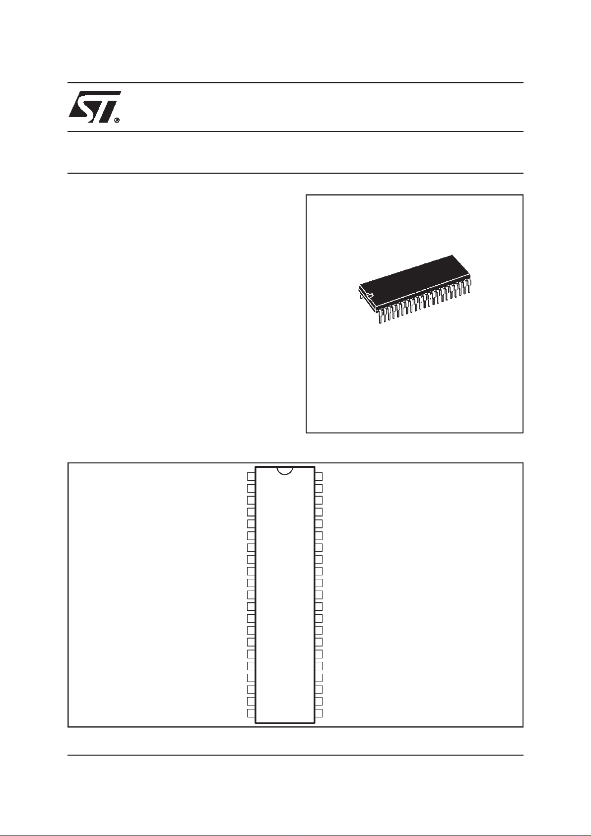
SHRINK42
(PlasticPackage)
ORDER CODE :
STV2112B
STV2112B
PIN CONNECTIONS
CHROMA/SCANNING GROUND
CHROMA LOOP FILTER
ACC CONTROL CAP ACITOR
CLOCHE FILTER TUNING
VOLUME AND MUTE CONTROL VOLTAGE
IF STANDARD AND SWITCH S ELECTION
EXTERNAL BLUE INPUT
EXTERNAL GREEN INPUT
EXTERNAL RGB INSERTION
CVBS OR LUMINANCE INPUT
XTAL2 SELECTION
4.43MHz XTAL
DATAWIRE I
CLOCK WIRE I
OSD GREEN INPUT
OS D RGB INSERTION
EXTERNAL RED INPUT
2
C BUS
2
C BUS
FILTER TUNING
OS D BLUE INPUT
OS D RED INPUT
ACC
SDA
SCL
VOL
SWI
1
2
3
4
5
6
7
8
9
10
11
12
13
14
15
16
17
18
19
20
21 22
GND2 V
SELECT
CXTL1
CLPF
FTUN1
FTUN2
BOSD
GOSD
ROSD
FBOSD
BEXT
GEXT
REXT
FBEXT
Y/CVBS
GND1
42
41
40
39
38
37
36
35
34
33
32
31
30
29
28
27
26
25
24
23
CC2
BYO
RYO
RYI
BYI
LFB/SC
HOUT
VOUT
VAMP
SLPF
SXTL
BCL
ICAT
RO
GO
BO
CR
CB
CG
CHR/SVHS
V
CC1
CHROMA/SCANNING/BUS SUPP LY
B-Y OUTPUT
R-Y OUTPUT
R-Y INPUT
B-Y INPUT
LINE FLYBACK INPUT/SANDCASTLE OUTP UT
HORIZONTAL OUTP UT
VERTICAL OUTPUT
AMPLITUDE CONTROL VOLTAGE
SCANNING LOOP FILTER
503kHz CERAMIC
BEAM CURRENT LIMITER
CATHODE CURRENT MEASUREMENT
RED OUTPUT
GREEN OUTPUT
BLUE OUTPUT
RED CUT-OFF CAPACITOR
BLUE CUT-OFF CAPACITOR
GREEN CUT-OFF CAPACITOR
CHROMINANCE INPUT/SVHS S ELECTION
VIDEO SUP PLYBUS/VIDEO GROUND
2112B-01.EPS
August 1998
1/24
Page 2

STV2112B
BLOCKDIAGRAM
CB
25
CG
24
CR
26
ICAT
30
R
G
292827
B
BCL
VOUT
VAMP34
31
35
HOUT
36
EXTERNAL OSD
15 14 13 12
FB RG BFBRGB
R-Y B-Y
STV2112B
BLANKING
AUTO CUT-OFF
BLACK&WHITE
RGB SWITCHES
Contrast
MATRIX
SATURATION
BRIGHTNESS
CONTROL
CONTRAST
FRAME
SCANNING
VIDEO
IDENTIFICATION
SYNC
SEPARATOR
LINE
CUT-OFF
DRIVE
STD
CONT
SAT
BRIG
BUS
SHARP
PAL
DEMODULATORS
SCANNING
DECODER
6 7 11 10
LFB/SC
SXTAL SLPF
SDA SCL
GND2 SWI VOLCLPF R-Y B-Y
2/24
CC2
V
CC1
22 42 19 18 17 1639 38
V
TUNING
CLOCHE
89
FILTER
TUNING
LINE
DELAY
SHARPNESS
Y
CLOCHE
FILTER TUNING
TRAP BANDPASS
20
Y/CVBS
SVHS SWITCH
23
CHR
STANDARD
IDENTIFICATION
ACC5
CHR
ACC
PAL
KILLER
KILLER
SECAM
DELAYLINE INTERFACE
SECAM
DEMODULATORS
PLL
2
3
CXTAL1
SELECT
21 1 373332
GND1
44041
2112B-02.EPS
Page 3

FUNCTIONAL DESCRIPTION
1 - DEFLECTIONCIRCUIT
Note :
[X,Y] : line number referred to the internal
line counternumbering
- Fully integratedsynch. separator , with a low pass
filter,a blacklevelalignm entof theY/CVBSinput,a
slicinglevelat2/3,1/3ofthesync.pulseamplitude.
- Frame sync. pulse locked on 2 f
frequency to
H
perfect interlace.
- 500kHzVCOwith an externalceramicresonator.
- Two phase locked loops
•
the first PLL locks theVCO on the video signal
frequency,
•
the secondPLLcompensatestheline transistor
storage time.
- Three time constantsfor the first PLL.
• thelongtimeconstantisusedfornormaloperation
• the short time constant is automatically used
duringthe frameretrace andin searchmodeof
VCRwhen the frame pulseis outside[258,264]
and [309,314].
• verylongtimeconstantwhennovideorecognition
Timeconstantsin normaloperation
(automaticselectionof timeconstants):
50Hz input signal:
- short time constant : [306,21]
- long timeconstant : the restof thefield
• inhibition of the firstPLL:
the first locked loop is openedfrom line 309 to
line 4.5 (or 314)in 50Hzmode.
• thetimeconstantsvaluesarechosenby means
of externalcomponents.
• possibility to force the short time constant
throughthe bus.
• possibility to force the very long time constant
throughthe bus.
- Video identification : coincidence detector between the line synchro top and a line frequency
windowfromthefirstPLL.The videoidentification
status isavailablein the output registerof theI
2
C
bus decoder.
- Generation of burst gate pulses and line frequency signals from the first PLL to drive the
chroma and video circuits. The burst gate pulse
is also sent to thesandcastlegenerator.
- Frame synchrowindow :
[248,352] catching
- Field frequencyselection windows:
[288,352] 50Hzmode selection window
- frame blankingpulse:
from line 0 to 21 in 50Hzmode
- Verticaloutputpulse is 10.5 lines long.
- Horizontal output pulse : 28µs line pulse on an
open collectoroutput;
- Start up circuit : the horizontaloutput is at a high
STV2112B
level when V
shutting down, horizontal pulses are disabled
when V
CC
- Soft-start circuit : the duty cycleof the horizontal
outputis78%(Thigh/(Thigh+TLow))whenV
is lower than(0.75x V
During the falling time, a 78% duty cycle HOUT
pulse is provided when V
(0.60 x V
CC2
- Possibility to disable the horizontal output pulse
through the bus (forcea high levelon HOUT).
- Horizontal position adjustmentcontrolledby bus.
- Bus controlledoutputvoltageto adjustthevertical
amplitude;thisvoltagepermitsto adjusttheslope
of the verticalsawtoothgeneratedbytheexternal
framebooster.
- Bus controlled vertical position ; the high level of
the vertical pulse permits to adjust the vertical
position.
- Bus controlled 4/3-16/9 selection : the low level
of theverticalpulseis 0.1Vwhen16/9 isselected,
2V when4/3 isselected.
- Combined flyback input and sandcastle output
(Pin 37). Two thresholdson LFB/SCOPin : The
lowestthreshold(0.7V) permitsto extractthe line
blanking pulse ; the highest threshold (2V) permits to extractthe line pulsefor PLL2. Thesandcastle signal at Pin 37 is used to control the
externalbasebandchroma delayline.
2 - FILTERS
- Integratedtrap filter:
f
−3dB
1
f
o
−
Q =
Center frequency :
- 4.43MHzfor PAL
- 4.25MHz,for SECAM (f
rejectionbetween 4.1MHzand 4.4MHz)
- Integratedchroma bandpass:
Q = 3.5, Centerfrequency=4.43MHz
- Integratedcloche filterfor SECAM:
Q = 16, Centerfrequency = 4.286MHz
- Integrateddelay line : Bandwidth= 8MHz
- Integratedlow pass filter for deflectionpart.
- Allfil t ersaretunedwitharefer e ncephaselockedloop.
ThePLLconsistsofa lowpassfilter,aphasecomparator,a loopfilter(withanexternalcapacito r) .Thereferencesign alisthecont i nuouscarr i erwavefromthe
VCO (4.43MHz). The PLL adjusts the center frequency of the lowpass so that it is equal to the
referencesignal.ThetuningvoltageofthePLLisused
toadjustallotherfilters.Theclochefilterisfinetuned
withasecondPLLoperatingduringframeretrace.
increases from 0 to 6.8V. On
CC
isbelow 6.2V.
),duringtherisingtime.
CC2
CC1
).
Q = 1.7 at sharp.min
f
−
3dB
f
o
Q =3.0 atsharp. max
= 3MHz; -20dB
-3dB
CC1
is lower than
3/24
Page 4

STV2112B
FUNCTIONAL DESCRIPTION(continued)
3 - VIDEO CIRCUIT
- 2 RGB inputs : RGB (OSD) input has priority
against the RGBext. Maximum contraston RGB
(OSD).-12dB range contrast controlonRGBext.
Possibility to disable the RGBext insertion
throughthe bus.
- Oversizeblanking capabilityon FB(OSD)(Pin15)
input. TheRGB ouputswill be blankedwhenthe
voltage on Pin 15 willexceed the secondthreshold at1.9V (blanking threshold) : the wholefield
is blankedbutnottheinsertedcut-offpulses.The
OSD insertionthresholdis0.7V.
- Automaticcut-off current loop : 2V cut-off range.
Sequential cut-off current measurement during
the three lines after the frame blanking signal.
Leakage currentmeasurement during the frame
blanking,memorizationon an internalcapacitor.
- Warm up detector.
- Beam current limiterDC voltageinput.
The beam current limiter control voltage will act
on contrast first, then the brightness will be decreasedwhencontrastattenuationreaches-5dB.
- Bus control of the red, green and blue channel
gain (Whitepoint adjustment)
- Bus controlof the red andgreenDC levels(black
point adjustment)
- PALand SECAM matrix).
- Switch-off of the trapfilterin SVHS mode.
- Buscontrolledcontrastonluminance(20dBrange)
- Bus controlledsaturation (50dBrange)
- Bus controlled brightness : 40% range at maximum contrast.
- Bus controlled sharpness (peaking) ; sharpness
active in PALstandardonly.
- Noise coring function on sharpness.
4 - CHROMA CIRCUIT
4.1 - PAL/SECAMDecoders
- SVHSinputs ; bus controlledSVHS mode.
- 30dB range ACC
- Use of an external ba se b and de lay line
(STV2180 recommended)
- Automaticstandard identification,with possibility
to forcethe standardthroughthe bus.
4.2 - PALDecoder
- ACC done by peak detector on synchronousdemodulationof the burst
- Fully integratedkillerfunctions.
- VCO using crystal4.43MHz
XTALSPECIFICATION:
Frequency:
4.433619MHz(PAL/SECAM)
Vibrationmode :Fondamental,seriesresonance
(no serial capacitor)
Motional capacity : 13fF ±3fF
Resonance resistance: < 70Ω
Shunt capacitance: < 7pF
Spuriousresponse: Noresonance at 3*f
o
and±90odemodulationangles forPAL
-0
±3kHz
o
4.3 - SECAMDecoder
- ACC
- Fully integratedkiller
- Two integrateddiscriminatorswith two PLL
- Integrateddeemphasis
4.4 - StandardIdentification
- Sequentialidentification.
- 2 identificationsequences:
PALmode, SECAMmode
- PALpriority
- the SECAM mode is locked after two identified
SECAMsequences
- the SECAM mode can be selectedin 50Hzonly
- Blanking of the (R-Y) and B-Y) outputs during
color searchmode.
5 - OTHER FUNCTIONS :
IF CONTROLS
5.1 - VolumeControl and Mute
Thevolumecontrolvoltagerangeon Pin10is from
0.5V to5V.
Alow voltageon Pin 10 (below 0.2V)will mute the
FM demodulatorof the IF circuit STV8224.
It will put thevolumeat theminimumleveland thus
there willbeno soundeitherinTVmodeor SCART
mode.
The volume control voltageand the mute levelare
controlledby the bus.
5.2- IF Standardand TV/SCARTMode Selection
The selection of IF standard (positive or negative
visionmodulation)andtheTV/SCARTmode iscontrolledbythe bus.Theselectionis convertedinfour
voltageson Pin 21.
The lowest voltage selects the TV mode and the
NEGATIVEvision modulation.
The highest voltage (open collector output with
internalpull-upresistorto V
) selects the SCART
CC
mode and the NEGATIVE vision modulation.
The two other intermediate voltages select either
TV mode and POSITIVE vision modulation or
SCARTmode and POSITIVEvision modulation.
4/24
Page 5
STV2112B
I2C BUS SPECIFICATION
GeneralComments
SlaveAddress: 8A(HEX)(1000101X)
WRITEMODEDATAFORMAT
Slave Address Register Address Data
1000 1010
(8A)
Thenot usedbits in data byte mustbe put to ”0”.
READ MODEDATAFORMAT
Slave Address Data
1000 1011
(8B)
MSB on the left, LSB on the Right.
MSB LSB
XXXXXXXX
X: not significantbit - S : significantbit
XXXS SSSS
(from 00 to 11HEX)
XXSS SSSS
(6 significant bits Max.)
SSSS SSSS
(8 significant bits)
InputSignals
(Write Mode)
VIDEO
Address
Dec (HEX)
0 (00) Contrast 5 XXX0 0000 = -20dB
0 (00) External Fast Blanking Enable 1 XXSX XXXX
1 (01) Saturation 6 XX00 0000 = -44dB
2 (02) Brightness 5 XXX0 0000 = -20%
2 (02) RGB Outputs Blanking 1 XXSX XXXX
3 (03) Red Drive Adjust (white point red adjust) 6 XX00 0000 = -6dB
4 (04) Red Cut-off Adjust 6 XX00 0000 = +150mV
5 (05) Green Drive Adjust (white point green adjust) 6 XX00 0000= -6dB
6 (06) Green Cut-off Adjust 6 XX00 0000 = +150mV
7 (07) Blue DriveAdjust (white point blueadjust) 6 XX00 0000 = -6dB
8 (08) Sharpness 3 XXXX X000 = Peaking Min.
Description
Data
(Bits)
Comments
XXX1 1111 = 0dB
0 = RGBext insertionenable
1 = RGBext insertiondisable
XX11 1111 = +6dB
XXX1 1111 = +20%
0 = Normal mode
1 = Blanking active
XX11 1111 = 0dB
XX11 1111 = -150mV
XX11 1111 = 0dB
XX11 1111 = -150mV
XX11 1111 = 0dB
XXXX X111 = PeakingMax.
5/24
Page 6

STV2112B
I2C BUS SPECIFICATION(continued)
InputSignals (Write Mode) (continued)
CHROMA
Address
Dec (HEX)
9 (09) Not used
10 (0A) Standard Selection 4 XXXX SSSS
10 (0A) SVHS Selection 1 XXXS XXXX
Description
Data
(Bits)
0000 = PAL/XTAL1 (4.43MHz)
0100 = SECAM/XTAL1
011X = Auto/90
0001 = Not allowed
0010 = Not allowed
0011 = Not allowed
0101 = Not allowed
1000 = Not allowed
1001 = Not allowed
1010 = Not allowed
1011 = Not allowed
111X = Not allowed
1100 = Not allowed
1101 = Not allowed
0 = No SVHS (CVBS mode)
1 = SVHS mode
Comments
o
DEFLECTION
Address
Dec (HEX)
11 (0B) Horizontal Shift 6 XX00 0000 = -2.5µs
12 (0C) Vertical Amplitude 6 XX00 0000 = 1.2V
13 (0D) Vertical Position 3 XXXX X000 = 3.8V
13 (0D) 50/60Hz Selection 2 XXXS SXXX
13 (0D) Horizontal Output (HOUT) Safety 1 XXSX XXXX
14 (0E) PLL1 Time Constant 2 XXXX XXSS
14 (0E) Interlace 1 XXXX XSXX
14 (0E) 4/3 16/9 Selection 1 XXXX SXXX
Description
Data
(Bits)
XX11 1111 = +2.5µs
XX11 1111 = 6.2V
XXXX X111 = 6.3V
00 = Automode
01 = Not allowed
10 = 50Hz
11 = Not allowed
0 = Normal mode
1 = HOUT disabled (high level)
00 = Normal mode (Auto)
01 = Short time constant
10 = Very long time constant
11 = PLL1 inhibition(open loop)
0 = Interlace
1 = DE-Interlace
0 = 4/3 (V
1 = 16/9 (V
OUT-Low
OUT-Low
Comments
= 2V)
= 0.1V)
6/24
Page 7

I2C BUS SPECIFICATION(continued)
InputSignals (Write Mode) (continued)
OTHERS
Address
Dec (HEX)
15 (0F) Volume 6 XX00 0000 = 0.5V
16 (10) Mute 1 XXXX XXXS
16 (10) IF Standard / AV Switch 2 XXXX XSSX
16 (10) Not Used 1 XXXX SXXX
16 (10) Cut-off Pulse Position 1 XXXS XXXX
17 (11) Only for Test 6 XXSS SSSS
Description
Data
(Bits)
XX11 1111 = 5V
0 = Mute not active
1 = Mute active
00 = INT/FM (negative)
01 = INT/AM (positive)
10 = EXT/AM (positive)
11 = EXT/FM (negative)
S = 0 default value
0 = lines 23/24/25in50Hz, 1 = Not allowed
00 0000 = Test mode notactive
STV2112B
Comments
OutputSignals
(ReadMode)
READ REGISTER
Description Data (Bits) Comments
Field Frequency 1 XXXX XXXS
Video Identification 1 XXXX XXSX
SVHS Status 1 XXXX XSXX
Standard Status 3 XXSS SXXX
Circuit Identification 2 SSXX XXXX
1 = 50Hz
0 = not 50Hz
1 = No Identification
0 = Video Identification
1 = No SVHS
0 = SVHS
111 = PAL/XTAL1 (4.43MHz)
110 = not to be used
101 = SECAM/XTAL1
011 = not to be used
010 = not to be used
X00 = Color off
11 = STV2118A/2116/2112
10 = STV2116A
01 = STV2112B
00 = STV2216
7/24
Page 8
STV2112B
I2C BUS SPECIFICATION(continued)
Bus Register Initial Conditions
Notused bitsare presetto ”0”.
Address
Dec (HEX)
0 (00) XX01 0000 Mid. contrast ; RGBext insertionenable
1 (01) XX10 0000 Mid. saturation
2 (02) XX01 0000 Mid. brightness ; Blanking :normal mode
3 (03) XX10 0000 Mid. RED driveadjust
4 (04) XX10 0000 Mid. RED cut-off adjust
5 (05) XX10 0000 Mid. GREEN drive adjust
6 (06) XX10 0000 Mid. GREEN cut-offadjust
7 (07) XX10 0000 Mid. BLUE drive adjust
8 (08) XX00 0100 Mid. sharpness
9 (09) XX10 0000 Not used
10 (0A) XX00 0110 Auto search color standard ; no SVHS
11 (0B) XX10 0000 Mid. horizontal shift
12 (0C) XX10 0000 Mid. vertical amplitude
13 (0D) XX00 0100 Mid. vertical position ; Auto search field frequency ; HOUT : normal mode
14 (0E) XX00 0000 PLL1 time constant : normal mode ; Interlace; 4/3 selection
15 (0F) XX10 0000 Mid. volume
16 (10) XX00 0000 Mute not active ; INT/FM IF mode; Not used ;
17 (11) XX00 0000 Test mode not active
Data Initial
Value
Comments
Cut-off pulses on lines23/24/25 in 50Hz
8/24
Page 9

STV2112B
ABSOLUTE MAXIMUMRATINGS
Symbol Parameter Value Unit
V
CC
T
oper
T
stg
Supply Voltage(Pins 22-42) (V
Operating Temperature 0, +70
Storage Temperature -55, +150
THERMALDATA
Symbol Parameter Value Unit
R
th(j-a)
Junction-ambient Thermal Resistance (PD= 1.3W) Typ. 40
CC1(22)
≤ V
)12V
CC2(42)
o
C/W
o
C
o
C
2112B-01.TBL
2112B-02.TBL
ELECTRICALCHARACTERISTICS
(V
CC
=9V,T
=25oC, unless otherwisespecified)
amb
Symbol Parameter Test Conditions Min. Typ. Max. Unit
SUPPLY
V
V
I
CC1
I
CC2
P
Video Supply Voltage (V
CC1
Chroma & Scanning & Bus Supply Voltage 8.1 9 9.9 V
CC2
V
Current Consumption 55 75 95 mA
CC1
V
Current Consumption PAL mode 50 70 90 mA
CC2
Power TotalDissipation 1305 1700 mW
tot
CC1
≤ V
) 8.1 9 9.9 V
CC2
LUMINANCE /CVBS INPUT (Pin 20)
DC
V
20PP
DC Operating Voltage No input signal 3.55 3.7 3.95 V
20
CVBS or Y Input Voltage 1 1.41 V
GY Luma Gain Contrast Max., Drive Max. 4.1 -
CTRY Luma Contrast Range 18 20 22 dB
-I
I
Negative ClampingCurrent During sync. pulse -20 -25 -35 µA
20
Clamping Current 5 10 µA
20
COMBINED CHROMINANCE ANDSVHS SELECTION INPUT (Pin 23)
V
V
CLIP23
V
DC23
V
TH23
I
low23
V
min23
G
Killer Colour Killer on Threshold
Chrominance Input Voltage Burst Amplitude,
23
100/75 colourbar
0.3 V
Input Amplitudebefore Clipping 1.0 V
DC Voltage SVHS mode 1.6 V
SVHS Threshold Voltage 0.5 0.7 V
Output Current 0V at Pin 23 120 170 µA
Minimum Burst Signal Amplitudewithin
30 mV
the ACC Control Range
ACC Control Range Change of Burstover whole
ACC
ACC control range < 2dB
30 dB
Burst amplitude on Pin 20 or
5
Pin 23, S/N > 40dB
Colour killer off hysteresis
+3
RGB INPUTS (Pins 12-13-14-16-17-18)
V
CLAMP
V
G
CTR
∆Black Difference of Black Level of Internal and
Clamp Level Contrast Max., Drive Nom. 1.5 1.8 2.1 V
RGB Input Voltage 0.7 1 V
RGB
RGB Gain Contrast Max., Drive Max. 4.0 -
RGB
RGB Contrast Range On external RGB (16-17-18) 11.5 dB
RGB
200 mV
External signals at the Outputs
I
RGB
Clamping Current 60 100 140 µA
mV
PP
PP
PP
PP
PP
dB
PP
2112B-03.TBL
9/24
Page 10

STV2112B
ELECTRICALCHARACTERISTICS
(V
CC
=9V,T
=25oC, unless otherwisespecified) (continued)
amb
Symbol Parameter Test Conditions Min. Typ. Max. Unit
OSD FAST BLANKING INPUT (Pin 15)
V
THFB1-15
V
THFB2-15
T
swi1-15
T
swi2-15
I
FB-15
Insertion ThresholdVoltage 0.5 0.7 0.85 V
Blanking ThresholdVoltage 1.6 2.0 2.4 V
Insertion Switching Delay 30 ns
Blanking Switching Delay 50 ns
Input Current 0V at Pin 15 50 µA
EXTERNAL FAST BLANKING INPUT (Pin 19)
V
THFB-19
I
FB-19
T
swi-19
Threshold Voltage 0.5 0.7 0.85 V
Input Current 0V at Pin 19 50 µA
Switching Delay 30 ns
CATHODE CURRENT INPUT (Pin 30)
V
LEAK
V
Coff
V
SB
I
Low-30
Leakage Current Reference Voltage 1.80 2.0 V
Cut-off Current Reference Voltage
250 mV
refered to Leakage Current Reference
Start Beam Current Detection
2.1 2.3 V
Reference Voltage
Source current 150 250 µA
AUTOMATIC CUT-OFF CAPACITORS(Pins 24-25-26)
I
24-25-26
Control Current 70 100 130 µA
BEAM CURRENT LIMITER VOLTAGE (Pin 31)
V
TH1-31
V
TH2-31
V
TH3-31
CTR-BCL Contrast Attenuation at V
V
TH4-31
BRIG-BCL BrightnessAttenuation at V
CLP
Contrast Attenuation Starting 6.0 V
Brightness Attenuation Starting 5.5 V
Contrast Attenuation Ending 5.0 V
31=VTH3-31
14.0 dB
Brightness Attenuation Ending 4.5 V
31=VTH4-31
High ClampingVoltage 6.5 V
31
100 %
RGB OUTPUTS (Pins 27-28-29)
V
BW
Output SignalAmplitude (B to W) 0.7V B/W at Pin 20, Drive Max.,
Contrast Max., Brightness Typ.,
2.85 V
Saturation Typ.
I
S27-28-29
V
M27-28-29
V
Black27-28-29
Output SinkingCurrent 1.5 2 mA
Maximum Peak White Level 7.8 V
Blanking Level No load 0.3 0.45 0.6 V
RCO Cut-off Output Range 2 2.6 V
DCCO Cut-off Adjustment Range On Red and Green ouputs
300 mV
Pins 29 and 28, Drive Max.
DRIV Drive Adjustment Range 6.5 dB
R BRIG BrightnessRange Relative to B/W amplitude on
30 40 50 %
R,G,B outputs at Contrast Max.
∆V
∆V
∆V
CTR
SAT
REL
Variation of Black Level with Contrast 100 mV
Variation of Black Level with Saturation 50 mV
Relative Variation in Black Level
between the three Channels
- during Variation of Contrast(20dB)
- during Variation of Brightness
(total range)
Drive Max.
0
10
5
2040mV
- during Variation of Vcc (+/-10%)
∆VTemp Black Level Thermal Drift 1 mV/
mV
mV
o
C
2112B-04.TBL
10/24
Page 11

STV2112B
ELECTRICAL CHARACTERISTICS
(V
CC
=9V,T
=25oC, unlessotherwisespecified)(continued)
amb
Symbol Parameter Test Conditions Min. Typ. Max. Unit
RGB OUTPUTS (Pins 27-28-29) (continued)
Track Tracking between Luminance and
Chrominance Signals
From Max. contrast (0dB)
to -10dBcontrast
2dB
Bwidth Bandwith of Output Signals at -3dB
- CVBS Input (no SVHS) PAL
- CVBS Input(no SVHS) SECAM
- Y Input SVHS Mode
- RGB Inputs
S/N Signalto Noise Ratio of Output (V
4.43MHz PAL Signal
on Y/CVBSInput
PP/VRMS
= 4.43MHz, Sharp Typ.
f
OSC
= 4.43MHz, no sharp
f
OSC
No trap Filter, Sharp Typ.
)
No signal on R-Y, B-Y inputs
Contrast Max., Drive Max.,
Saturation Typ., Sharp Typ.,
3.6
3.0
8
8
50 dB
Bandwidth 5MHz
Res Residual Frequency atf
at 2f
and Higher Harmonics
OSC
OSC
PAL/SECAM
PAL/SECAM
25
10
10050mV
FILTERS
V
V
TUN1
TUN2
Tuning Voltage Range (Pin 8) 3.2 to 4.8 V
Cloche Tuning Voltage Range (Pin 9) 2.5 to 6.5 V
Y DELAYLINE
t
t
d1p
t
d2
d3p
t
d4
Delay TimePAL SVHS mode 330 370 400 ns
Delay TimeSECAM SVHS mode 500 540 580 ns
Delay TimePAL CVBS mode 390 425 460 ns
Delay TimeSECAM CVBS mode 550 590 630 ns
SHARPNESS CIRCUIT (PAL only)
f
G
Sharp
Sharp
Center Frequency SVHS mode 2.5 MHz
Gain Variation from Min. to Max.Sharp at f
Sharp
6dB
Overshoot Amplitude Variation compared to B/W 2T pulse, Sharp Max. 150 %
Pre-shoot Amplitude Variation compared to B/W 2T pulse, Sharp Max. -15 %
After-shoot Amplitude Variation compared to B/W 2T pulse, Sharp Max. -40 %
Coring Coring Range comparedto B/W 10 %
Y TRAPFILTER
f
Trap
Trap Frequency PAL -0.2 f
OSC
+0.2 MHz
Trap Frequency SECAM -0.2 4.25 +0.2 MHz
Q
Trap
Trap Quality Factor
(Q=1/(fo/f-3dB - f-3dB/fo))
Sharpness Min.
Sharpness Max.
1.7
3
CRejPN Color Subcarrier Rejection PAL mode, Sharpness Min. 20 dB
CrejS Color Rejection SECAM Mode at 4.1MHz
at 4.4MHz
18
18
CHROMINANCE BANDPASS
f
Q
Center Frequency -0.25 f
C
Bandpass Quality Factor 2.8 3.5 4.2 -
BP
osc
+0.25 MHz
CLOCHE FILTER
f
Cloche
Q
Cloche
Resonant Frequency 4.286 MHz
Cloche Quality factor 14 16 18 -
ACC CAPACITOR (Pin 5)
I
C5
I
L5
Charging Current During burst gate window 250 µA
Leakage Current 0.2 1 µA
CHROMA PLL (Pins 2-3)
CR
Catching Range Q = 4.43MHz (Pin 3) ±600 Hz
2-3
MHz
MHz
MHz
MHz
mV
dB
dB
PP
PP
-
-
2112B-05.TBL
11/24
Page 12

STV2112B
ELECTRICALCHARACTERISTICS
(V
CC
=9V,T
=25oC, unless otherwisespecified) (continued)
amb
Symbol Parameter Test Conditions Min. Typ. Max. Unit
PLL LOOP FILTER (Pin 4)
I
I
Control Current During burstgate window 400 µA
C4
Leakage Current 5 µA
L4
COLOR DIFFERENCE OUTPUT SIGNALS (Pins 40-41)
PAL DEMODULATOR
o
V
V
G
V
P40
P41
PAL
PNDC
R-Y Outputsignal Amplitude (Pin40) |RED-BLUE| axes = 90
100/75 colour bar
B-Y Output SignalAmplitude (Pin 41) |RED-BLUE| axes = 90
100/75 colour bar
Gain Ratioof both Demodulators (B-Y)/(R-Y) |RED-BLUE| axes = 90
100/75 colour bar
Output Voltagewhen colourkilled 5.6 5.8 6.0 V
0.40 0.52 0.60 V
o
0.50 0.66 0.80 V
o
1.15 1.27 1.45 -
SECAM DEMODULATORS
V
V
G
SECAM
V
R-Y OutputSignal Amplitude (Pin40) 100/75 Colour Bar 0.8 1.05 1.20 V
S40
B-Y Output SignalAmplitude (Pin 41) 100/75 Colour Bar 1.00 1.33 1.40 V
S41
Gain Ratioof both Demodulators (B-Y)/(R-Y) 1.00 1.27 1.35 Output Voltagewhen colourkilled 5.4 5.6 5.8 V
SDC
PAL /SECAM MATRIX
G/R (G-Y)/(R-Y) -0.6 -0.51 -0.4 -
G/B (G-Y)/(B-Y) -0.28 -0.19 -0.15 -
SATURATION CONTROL
SAT
SAT
SAT
Maximum Saturation Control (3F) 1VPPCVBS on Pin 20 5 +6.5 8 dB
Max.
Nominal Saturation Control (20) 1VPPCVBS on Pin 20 0 dB
Nom.
Minimum SaturationControl(00) 1VPPCVBS on Pin 20 -44 dB
Min.
COLOUR DIFFERENCE INPUT SIGNALS (Pins 38-39)
DCRYI DC Voltage Pin 39 No colour 2.6 2.8 3.0 V
DCBYI DC Voltage Pin 38 No colour 2.6 2.8 3.0 V
VRYI Input SignalAmplitude Pin 39 100/75 color bar 1.05 V
VBYI Input SignalAmplitude Pin 38 100/75 color bar 1.33 V
I
CL38-39
Clamping Current During burst key 150 µA
SYNC. SEPARATOR
VSync Sync. Pulse Amplitude On Pin 20 50 300 mV
HORIZONTAL OSCILLATOR
f
f
Rang
f
Frequency afterDivider 50Hz input signal 15625 Hz
H50
Frequency Control Range Low Frequency
Free RunningFrequency when PLL1 open Value 03hex
free
High Frequency
in register0Ehex
14500
16100
14850
16300
15000 15800 Hz
15200
16500HzHz
FIRST LOOP FILTER (Pin33)
I
LOW-33
I
HIGH
I
VLOW
Long TimeConstant Output Current 0.12 0.15 0.18 mA
Short TimeConstant Output Current 0.35 0.45 0.55 mA
Very LongTime Constant 0.02 0.03 0.05 mA
SECOND CONTROL LOOP
CRQ
t
shift
Control Range from Startof Horizontal
2
Output toFlyback
Horizontal Shift Range 4 µs
Horizontal position
centered
2to 14 µs
PP
PP
PP
PP
PP
PP
2112B-06.TBL
12/24
Page 13

STV2112B
ELECTRICALCHARACTERISTICS
(V
CC
=9V,T
=25oC, unless otherwisespecified) (continued)
amb
Symbol Parameter Test Conditions Min. Typ. Max. Unit
LINE FLYBACKINPUT/SANDCASTLE OUTPUT (Pin 37)
V
V
t
t
V
TH1-37
V
TH2-37
SCO
CL37
WBG
dBG
I
Output Voltageduring Burst Key 4.0 5.0 V
Clamped Input Voltage during Flyback 2.5 3.1 V
Burst KeyPulse Width 3.7 3.8 3.9 µs
Delayof Start of Burst Keyto Startof Sync. 5.2 µs
Blanking ThresholdVoltage 0.5 0.7 0.9 V
PLL2 ThresholdVoltage referred to Line
Level V
CL37
Input Current During flyback pulse 0.1 1 mA
37
PLL2VTH/V
CL37
80 %
HORIZONTAL OUTPUT (Pin 36)
T
W36
V
Low36
V
CC StartVCC Start
V
CC StopVCC Stop
I
36 Max.
V
36 Max.
T
Output PulseWidth Normal operation 26 28 30 µs
Voltage Output Low R pull-up = 1kΩ 1.1 V
Level Voltage on Pin 42 6.7 V
Level : hysteresis Voltage on Pin 42,
V
CCstart-VCCstop
0.60 V
Maximum Allowed Output Current 10 mA
Maximum Allowed Output Voltage
(open collector)
Output PulseDuty Cycle in soft-start
ss
mode (Thigh/(Thigh + Tlow))
V
(V
CC2
CC1
= 9V, V
rising)
CC1
< 6.0V
78 %
12 V
VERTICAL OUTPUT (Pin 35)
T
V
Low35
W35
Output PulseWidth 10.5 Lines
Low Level Output Voltage 4/3
Low Level Ouput Voltage 16/9
XXXX0XXX (bin)in Reg. 0Ehex
XXXX1XXX (bin)in Reg. 0Ehex
1.5 2
0.1
2.5
0.5
FR35 Locking Range 248 352 Lines
f
FR-50
V
HIGH35
I
sink
Free Frequency (no Video Signal) 50Hz 314 Lines
High Level Range
(vertical position control)
Output SinkingCurrent 4/3
XXXXX000(bin) in Reg. 0Dhex
XXXXX111(bin) in Reg. 0Dhex
16/9
3.5
5.7
3.8
6.3
0.2
0.5
4.2
7.0
VERTICAL AMPLITUDE CONTROL (Pin 34)
V
Output VoltageRange XX000000(bin) in Reg. 0Chex
34R
XX111111(bin) in Reg. 0Chex
1.0
5.6
1.2
6.2
1.5
6.7
VOLUME CONTROL AND MUTE (Pin 10)
V
Output VoltageRange
R10
(volume control)
XX000000(bin) in Reg. 0Fhex
XX111111(bin) in Reg. 0Fhex
0.35
4.2
0.5
4.7
0.7
5.2
MUT Output Voltage when MUTE 0.02 0.1 V
V
V
V
V
mA
mA
V
V
V
V
2112B-07.TBL
13/24
Page 14

STV2112B
ELECTRICAL CHARACTERISTICS
(V
CC
=9V,T
=25oC unlessotherwisespecified)(continued)
amb
Symbol Parameter TestConditions Min. Typ. Max. Unit
IF STANDARD CONTROL & SWITCH SELECTION (Pin 11)
V
TV/NEG
V
TV/POS
V
Start/Pos
V
Start/Neg
R
TV/Neg
R
TV/Pos
R
Scart/Pos
R
Scart/Neg
2
I
C BUS INPUTS (Pins6-7)
V
TH6-7
C
I
Leak6-7
Output Voltagein TV Mode and
Negative Vision Modulation
Output Voltagein TV Mode and
Positive VisionModulation
Output Voltagein SCART Mode and
Positive VisionModulation
Output Voltagein SCART Mode and
Negative Vision Modulation (open collector mode)
Output Resistance in TV Mode and
Negative Vision Modulation
Output Resistance in TV Mode and
Positive VisionModulation
Output Resistance in Scart Mode and
Positive VisionModulation
Output Resistance in Scart Mode and
Negative Vision Modulation (pull-up resistorto V
Threshold Voltage 1.5 2.25 3 V
Capacitance of each Pin 5 10 pF
L6-7
Leakage Current Write Mode,
VCC= 9V 0.1 0.7 V
VCC= 9V 2.90 3.37 3.80 V
VCC= 9V 5.20 5.62 6.10 V
VCC= 9V 7.88 9 V
200 Ω
6.7 kΩ
11 kΩ
18 kΩ
)
CC
0 levelon SDA or SCL
50 µA
2112B-08.TBL
14/24
Page 15

USER CONTROLS
Figure1 : ContrastControl Curve
%
120
STV2112B
Figure2 : SaturationControl Curve
%
250
100
80
60
40
20
0
00 10 1F
Code (HEX)
Figure3 : BrightnessControl Curve
%
30
20
10
0
(10)
(20)
200
150
100
50
0
00 20 3F
2112B-03.EPS
10 30
Code (HEX)
Figure 4 : PeakingControl (2T overshoot)
%
160
150
140
130
120
110
100
2112B-04.EPS
(30)
00 10 1F
Code (HEX)
Figure5 :
Output Voltage (Pin 10)
6
5
4
3
2
1
0
00 20 3 F
2112B-05.EPS
VolumeControlCurve
10 30
Code (HEX)
90
07
123 456
Code (HEX)
2112B-07.EPS
2112B-06.EPS
15/24
Page 16

STV2112B
INPUT/OUTPUTPIN CONFIGURATION
Figure6 : Pins2, 3 - CXTL1,SELECT
V
CC2
Pins 2-3
Figure7 : Pin 4 - CLPF
V
CC2
4
Figure8 :
Figure10 :
Pin 5 - ACC
Pin7 - SCL
V
CC2
GND2
GND2
V
CC2
GND2
2112B-08.EPS
Figure9 :
Pin 6 - SDA
V
CC2
2112B-09.EPS
6
5
2112B-10.EPS
Figure11 :
GND2
Pin8 - FTUN1
V
CC2
V
CC1
2112B-11.EPS
16/24
GND2
8
7
2112B-12.EPS
GND2
2112B-13.EPS
Page 17

INPUT/OUTPUTPIN CONFIGURATION(continued)
Figure12 : Pin9 - FTUN2
V
CC2
9
Figure13 : Pin10 - Volume
V
CC2
STV2112B
10
GND2
Figure14 : Pin11- SWI
V
CC2
11
GND2
Figure16 : Pins15,19 - FBOSD,FBEXT
V
CC1
GND2
2112B-14.EPS
Figure15 : Pins12,13,14,16,17,18- RGBInputs
V
CC1
Pins 12-13-14
16-17-18
2112B-16.EPS
GND1
Figure17 : Pin20 - Y/CVBS
V
CC1
V
CC2
2112B-15.EPS
2112B-17.EPS
GND1
Pins 15-19
20
2112B-18.EPS
GND1
2112B-19.EPS
17/24
Page 18

STV2112B
INPUT/OUTPUTPIN CONFIGURATION(continued)
Figure18 : Pin23 - CHR/SVHS
V
CC2
V
CC1
23
Figure19 : Pins24, 25, 26 - CG, CR, CB
V
CC1
Pins 24-25-26
30
Figure20 :
Figure22 :
V
CC1
GND2
Pins27, 28, 29 - BO,GO, RO
V
CC1
Pins 27-28-29
GND1
Pin31 - BCL
V
CC1
2112B-20.EPS
Figure21 :
2112B-22.EPS
Figure23 :
GND1
Pin30 - ICAT
GND1
Pin32 - SXTL
2112B-21.EPS
V
CC1
30
2112B-23.EPS
V
CC2
18/24
GND1
31
32
2112B-24.EPS
GND2
2112B-25.EPS
Page 19

INPUT/OUTPUTPIN CONFIGURATION(continued)
Figure24 : Pin33 - SLPF
V
CC2
33
Figure25 : Pin34 - VAMP
V
STV2112B
CC2
34
Figure26 :
Figure28 :
Pin 35 - VOUT
V
CC2
Pin37 - LFB/SC
GND2
V
CC2
GND2
35
2112B-26.EPS
Figure27 :
2112B-28.EPS
Figure29 :
GND2
Pin36 - HOUT
GND2
Pins38, 39 - BYI, RYI
V
CC2
V
CC1
2112B-27.EPS
V
CC2
36
2112B-29.EPS
GND2
37
Pins 38-39
2112B-30.EPS
GND2
2112B-31.EPS
19/24
Page 20

STV2112B
INPUT/OUTPUTPIN CONFIGURATION(continued)
Figure30 : Pins40, 41 - RYO, BYO
V
CC2
Figure31 : Pins42, 22 - V
CC2,VCC1
GND2
Pins 40-41
V
CC2
42
1
V
CC1
22
21
GND2 GND1
2112B-32.EPS
2112B-33.EPS
20/24
Page 21

APPLICATIONDIAGRAM
100nF
330kΩ
FROM
OSD
+
TXT
OBLK
(ove rsize
blan king)
FROM
EXTERNAL
RGB
TO Pin42
I2C BUS
TO STV8224
3.9k
3.9k
3.9k
2.2k
Ω
Ω
Ω
Ω
SDA
SCL
VOL
SWI
390
390
390
1kΩ
75
75Ω
75
270k
Ω
100Ω100
Ω
47pF
100
Ω
47pF
Ω
Ω
Ω
Ω
Ω
18k
Y/CVBS
Input 1V
Ω
4.7nF
PP
3.58MHz
1
3.3pF
2
3
4.43MHz
4
33nF
5
6
7
8
100nF
9
100nF
10
11
22nF
12
22nF
13
22nF
14
15
22nF
16
22nF
17
22nF
18
19
220nF
20
75
Ω
21 22
GND2
S ELEC T
CXTL1
CLPF
SDA
SCL
FTUN1
FTUN2
VOL
SWI
BOSD
GOSD
ROSD
FBOSD
BEXT
GEXT
REXT
FBEXT
Y/CVBS
GND1
F
470
µ
16V
100nF
S
T
V
2
1
1
2
B
CHR/S VHS
100nF
470
F
µ
16V
V
BYO
RYO
RYI
LFB/SC
HOUT
VOUT
VAMP
SLPF
S XTL
BCL
ICAT
V
STV2112B
9V
1
2
42
CC 2
10nF
41
10nF
40
10nF
39
10nF
38
BYIACC
37
36
35
34
33
503kHz
32
31
30
RO
29
GO
28
BO
27
100nF
CR
26
100nF
25
CB
100nF
CG
24
23
1k
CC 1
9V
1k
47k
470
470
470Ω
Ω
9V
Ω
Ω
Ω
Ω
10nF
TO
DEFLECTION
STAGES
F
1
µ
50V
220k
Ω
75
Ω
15k
Ω
1µF
4.7k
18k
Ω3.3nF
22k
Pin 22
CHROMA INPUT (S-VHS)
3
4
5
4.7nF
6
78
9V
4.7kΩ
Ω
1N4148
Ω
Pin 42
TO
CRT
AMPLIFIERS
S
T
V
2
1
8
0
100nF
14
13
12
11
100nF
10
9
Ω
680
1N4148
1N4148
100nF
1nF
LFB (He ater)
FROM
HORIZONTAL
STAGE
9V
4.02k
1%
10
Ω
F
47
µ
16V
Ω
75
Ω
Notes :
- STV2112B requires only 1 XTAL(4.43MHz).
- Recommended 4.43MHz XTAL is JAUCH Number 10080082.
- XTAL2 selection pin (Pin 2) : werecommend the connection toVCC2 (Pin 42).
Inthe case of STV2112B version, this pin can be left open.
2112B-34.EPS
21/24
Page 22

STV2112B
90oCRT APPLICATIONSVERTICALSTAGE
22
VOUT
(From STV2112B
Pin 35)
VAMP
(From STV2112B
Pin 34)
1k
+12V
15k
Ω
Ω
Ω
1000µF
25V
100nF
1N4148100k
47nF
47µF
25V
15k
3.9k
270
1.8kΩ
+9V
BC547
Ω
2W
Ω
Ω
Ω
27k
15k
Vertical Yoke
470
Ω
1000µF
25V
1.2
Ω
620k
620k
Ω
Ω
160k
330k
Ω
1.3k
Ω
Ω
Ω
220nF2.2
Ω
4.7k
1
OUT
2
V+
Ω
3
V.SYNC
4
V.SIZE
T
D
5
GND
Ω
47nF
6
SAW
A
1
7
7
7
10kΩ
8
BUFF
FEEDB
1
+9V
56k
470k
Ω
100k
Ω
BC557
OPTIONAL4/3 - 16/9 SWITCHING
4.7µF
100k
Ω
Ω
BC547
560k
9
V
100µF
Ω
+24V
1000µF
25V
35V1N4004
CC
10
FLYB
2112B-35.EPS
22/24
Page 23

110oCRT APPLICATIONS: Vertical System with East-West
CC
HFLY
220k
R28
100
C36
10nF
6.2k
R56
Ω
R45
Ω
R43
1k
Ω
+12V
Ω
V
CC
R2
10
3W
C5
2200µF
R46
100k
From
STV2112B
Pin35
+12V
+9V
C20
47µF
SCL
SDA
VOUT
R81
2.4k
100pFF
Ω
C34
T5
BC547
R52
4.7kΩ
C56
220nF
R3
330
Ω
R31
330
330
470
R18
R17
R30
Ω
1
SCL
Ω
2
SDA
Ω
3
VRET
S ENS M
SENS P
FROUT
100
16
15
14
S
REG
V
CC
LPF
CVER T
GND
T
V
2
1
4
5
4
V
CC
5
C44
220nF
6
C48
4.7nF
7
C51
33nF
89
EWOUT
EWIN
OBLK
HFLY
BREATH
13
12
11
10
C54
1nF R54
Vertical
Yoke
R19
1.2
Ω
R20
3.6
Ω
Ω
C39
10nF
C37
1nF
R57
22k
Ω
V
R55
100k
Ω
680k
Ω
Ω
C46
3.3nF
R50
1.5k
1N4148
Ω
D8
BCL
C4
1000µF
25V
T6
TIP122
Ω
V
CC
OBLK
R12
1.5
Ω
C10
220nF
R47
39k
Ω
R41
3.3k
Ω
To STV2112B
Pin15
+24V
D2
1N4148
D4
1N4148
C31
1.5nF
E/W MODULATOR
C68
4.7µF
160V
C43
22pF
1000µF
C23
100µF
D1
1N4004
R36
3.3k
10k
R26
35V
+24V
C9
Ω
Ω
STV2112B
IN-
1
V
2
CC
FLYBACK
3
GND
4
OUT
5
OUTV
6
CC
IN+
7
+12V
T
D
A
8
1
7
2
2112B-36.EPS
23/24
Page 24

STV2112B
PACKAGE MECHANICAL DATA
42 PINS - PLASTICSHRINK DIP
A2
A1
E
E1
LA
42
1
Dimensions
BeB1
D
22
21
c
SDIP42
Millimeters Inches
Min. Typ. Max. Min. Typ. Max.
e1
e2
E
.015
0,38
Gage Plane
e3
e2
A 5.08 0.200
A1 0.51 0.020
A2 3.05 3.81 4.57 0.120 0.150 0.180
B 0.36 0.46 0.56 0.0142 0.0181 0.0220
B1 0.76 1.02 1.14 0.030 0.040 0.045
c 0.23 0.25 0.38 0.0090 0.0098 0.0150
D 37.85 38.10 38.35 1.490 1.5 1.510
E 15.24 16.00 0.60 0.629
E1 12.70 13.72 14.48 0.50 0.540 0.570
e 1.778 0.070
e1 15.24 0.60
e2 18.54 0.730
e3 1.52 0.060
L 2.54 3.30 3.56 0.10 0.130 0.140
Information furnished is believed to be accurate and reliable. However, STMicroelectronics assumes no responsibility for the
consequences of use of such information nor for any infringement of patents or other rights of third parties whichmay result from
its use. No licence is granted by implication or otherwise under any patent or patent rights of STMicroelectronics. Specifications
mentioned in this publication are subject to change without notice. This publication supersedes and replaces all information
previouslysupplied.STMicroelectronicsproducts are notauthorizedfor use ascriticalcomponentsin lifesupport devicesor systems
without express written approval of STMicroelectronics.
The ST logo is a registered trademark of STMicroelectronics
PMSDIP42.EPS
SDIP42.TBL
1998 STMicroelectronics - All Rights Reserved
2
Purchase of I
Rights to use thesecomponents in aI
C Components of STMicroelectronics,conveys a licenseunder the PhilipsI2C Patent.
2
the I
C StandardSpecifications as defined byPhilips.
2
C system,is granted providedthat the system conformsto
STMicroelectronics GROUP OF COMPANIES
Australia - Brazil - Canada- China - France - Germany - Italy - Japan - Korea- Malaysia - Malta - Mexico - Morocco - The Netherlands
Singapore - Spain- Sweden - Switzerland- Taiwan- Thailand - UnitedKingdom - U.S.A.
24/24
 Loading...