

Page 1
STV2110B
PAL-SECAM LUMA-CHROMA& DEFLECTIONPROCESSOR
PRELIMINARY DATA
■
RGB ANDFAST BLANKINGINPUTS
■
AUTOMATIC CUT-OFF CONTROL
■
DC-CONTROLLED BRIGHTNESS, CONTRAST
AND SATURATION
■
CERAMIC 500kHz VCO FOR LINE DEFLECTION
■
CHROMA STANDARD AUTOMATIC IDENTIFICATION
■
BIDIRECTIONAL I/O FOR CHROMA STANDARD
■
PHASE-LOCKED REFERENCE OSCILLATOR
USING ASTANDARD 4.43MHz
■
OSD CAPABILITYON OUTPUTS
■
VIDEO IDENTIFICATIONGENERATOR
DESCRIPTION
The STV2110Bis a PAL-SECAMchromadecoder,
videoand H/V deflection processorfor CTV.
UsedwiththeTDA8222,this ICpermitsacomplete
lowcost solutionwith external output stages.
It is pincompatible with STV2102BPAL only processor.
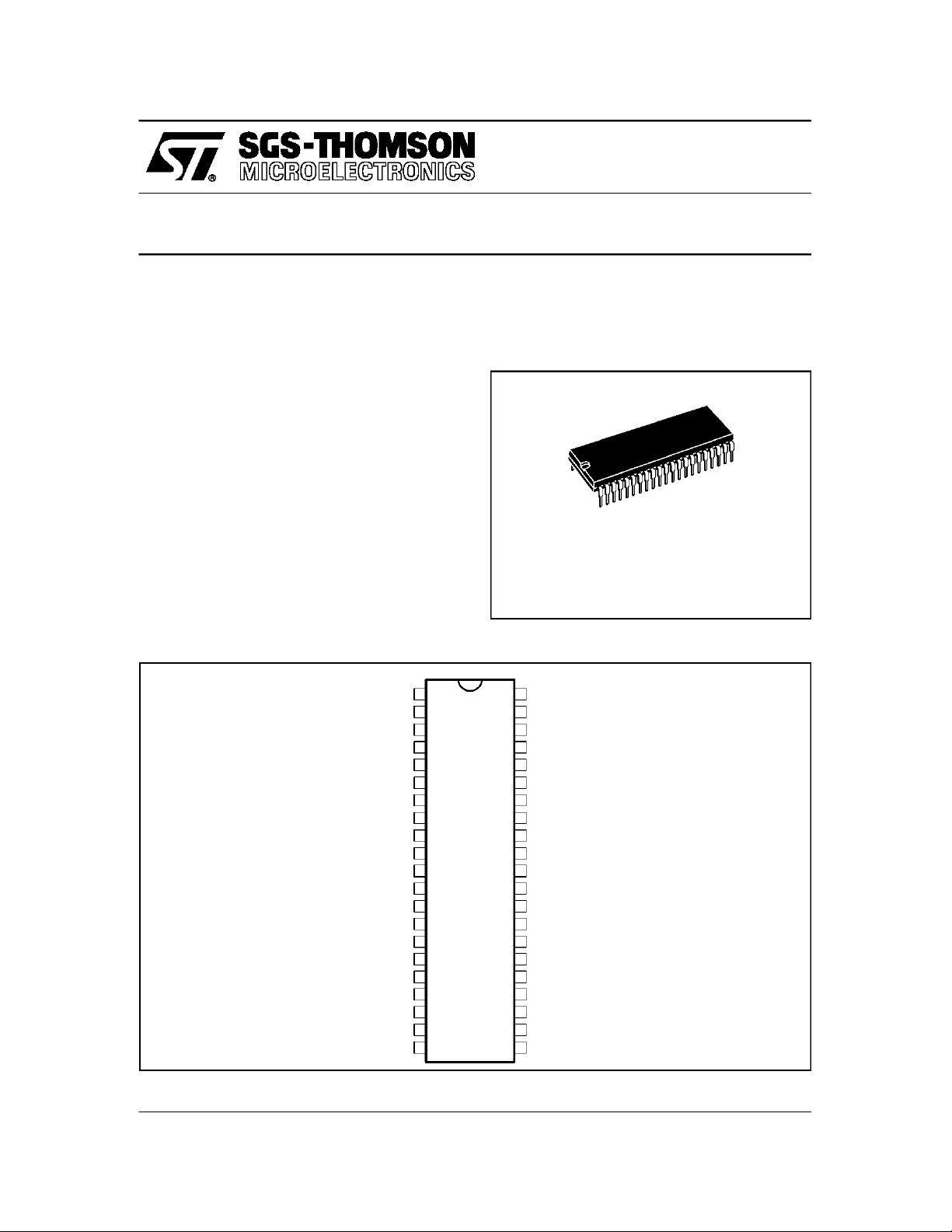
SHRINK 42
(Plastic Package)
ORDER CODE : STV2110B
PINCONNECTIONS
GREEN CUT-OFF CAPACITOR
SUPPLYVOLTAGE
HORIZONTAL Vcc
GREENOUTPUT
BLUE OUTPUT
BLUE CUT-OFF CAPACITOR
LUMINANCE SIGNAL INPUT
SCANNING LOOP FILTER
SCANNING XTAL
COMPOSITEVIDEO SIGNAL
LINE FLYBACK INPUT
VERTICAL OUTPUT
HORIZONTAL OUTPUT
CONTRAST CONTROL
SECAMCHROMA INPUT
GROUND GND
DELAY CHROMA INPUT
CHROMA STANDARD I/O
Vcc
BLKBLANKING INPUT
COG
ROUTRED OUTPUT
HVcc
GOUT
BOUT
COB
YIN
SLPF
SXTL
CVBS
LFB
VOUT
HOUT
CTR
SECIN
PALINPAL CHROMA INPUT
DLI
1
2
3
4
5
6
7
8
9
10
11
12
13
14
15
16
17
18
19
20
PS
21
ICAT CATHODECURRENT
42
SUPPLY VOLTAGE INPUT
Vcc
41
BLUE INPUT
BIN
40
GIN GREEN INPUT
39
RED CUT-OFF CAPACITOR
COR
38
RIN REDINPUT
37
BRIGHTNESS CONTROL
BRIG
36
FAST BLANKING INPUT
FBL
35
34
33
32
31
30
29
28
27
26
25
24
23
22
CHROMA LOOP FILTER
CLPF
CHROMA XTAL
CXTL
PAL KILLER CAPACITOR
CKP
F425
4.25MHzFILTER
ACC ACC CONTROLCAPACITOR
RED DEEMPHASIS CAPACITOR
CDR
4.40MHz FILTER
F440
SATURATION CONTROL
SAT
CDB
BLUEDEEMPHASIS CAPACITOR
F432 4.32MHz FILTER
GROUND
GND
CKS
SECAM KILLER CAPACITOR
CHROMA OUTPUT
DLO
2110B-01.EPS
April 1996
This is advance information on a new product now in development or undergoingevaluation. Detailsare subject to change without notice.
1/15
Page 2
STV2110B
BLOCK DIAGRAM
BRIG
CTR
BIN
GIN
RIN
FBL
SAT
35 16 36
ROUT
4
STV2110B
Blk. RGB
CONTRAST
GOUT
BOUT
6
7
BRIGHTNESS BLANKING
+ CLAMP
MATRIX
COR
COG
3388
RGB
CUT-OFF
MEAS.
LEAK. CURRENT
MEAS.
TUBE TEMP
RGB
SWITCH
SATURATION
COB
ICAT
42
BLK
2
BLANKING
COMPENSATION
DECODER
SEPARATOR
FRAME SYNC.
PAL
FLIP-FLOP
SECAM
DEMODULATION
VOUT
14
FRAME
OUTPUT
LINE
COUNTER
SECAM
FLIP-FLOP
SECAM
IDENTIFICATION
HOUT
15
LINE
OUTPUT
SHIFT
PHASE
PHASE
COMP. 2
BURST
GENERATOR
VCO
DIVIDER
PHASE
COMPARATOR 1
SYNC.
SEPARATOR
MUTE
PERMUTATOR
SAT
CONTROL
STANDARD
SXTL
SLPF
LFB
CVBS
F440
CDR
F432
CDB
F425
3121 26 29 28
CKS
23
PS
2/15
BLACK
INSERTION
CC
HV
5
CC
V
CC
V
YINPUT
CONTRAST
12741 37 39 40
9
YIN
BLACK
REFERENCE
CLAMP
PAL
DEMODULATION
XVCO
33
CXTL
– 90DEG
PHASE
DETECTOR
34
CLPF
KILLER
BURST
DETECTOR
30
ACC
32
CKP
DL
MATRIX
ACC
18
PALIN
17
SECIN
DLI
DLO
22 252024 1312 10 11
GND
19
GND
2110B-02.EPS
Page 3

FUNCTIONAL DESCRIPTION
DEFLECTION
SynchronizationSeparator
The synchronization separator is based on the
bottom of synchronizationpulses alignment to an
internal reference voltage. An external capacitor
permitstoalign synchro.pulses,two externalresistors determinesthe detectionthresholdof synchro
pulses. The frame synchronization pulses are
locked to a 32µs referencesignal to perfect interlacing.
HorizontalScanning
Thehorizontalscanningfrequencyisobtainedfrom
a 500kHz VCO. The circuituses twophase-locked
loops (PLL). The first onecontrols the frequency;
the second one, fully integrated, controls the relative phase of the synchronization and the line flyback signals.
The first PLLhas two times constants: a long time
constant during the picture to have a good noise
immunity, a short timeconstantat the beginningof
the frame to recapturefaster the phase in case of
VCR video signal. More over, the PLL is in short
time constantthree lines before frame pulses occured, it permits to ensure good interlacing when
the video signalcomes from a VCR tape with high
phase error.
The horizontal output signal is 28µs width. On
starting up, horizontal pulses are enabled at
= 6.8V. On shutting down, horizontal pulses
V
CC
are inhibited for V
CC
=6.2V.
VerticalScanning
The windows for the frame sync detection are
generatedby a count down system. Theselection
of the windows is determinedby the IC status :
- videoidentificationoff - window: 248/314
- videoidentificationon - window: 248/352
When a sync pulse is detected inside the window
a 10.5 lines longpulse is providedto V
OUT
pin.
The count downsystem provides also the needed
signals for the time constant switch, the line PLL
inhibitionand servicesignals to the rest of the IC.
CHROMA
ACC Amplifier, DL Matrix, Permutator and Demodulator
The correct chroma subcarrier input, issued from
bandpassorbellfilter,isinternallyselectedwith the
standa rd. The ACC amplifier envolves three
stages : the first one select the correct input, the
second one the -6dB in picture (PAL mode), the
third one is controledby the ACC voltage.
STV2110B
The dynamic rangeis over than 30dB.
The chrominance output signal is fed to the delay
line.
- PALmode :
the adding and substracting direct and delayed
signalsare performedby the DL matrix function.
Two synchronous demodulators multiplies
the (B-Y) signal with the 0 degree phase
4.43MHz reference signal and the (R-Y) signal
with the alternate ±90 deg. 4.43MHz phase referencesignal.
- SECAM mode :
thepermutatorseparatesthetwo(B-Y)and(R-Y)
subcarriers.These signals are demodulatedby
two FM demodulators with two external L, C
centered on f
4.406MHz.
4.43MHz Phase Locked Loop
The oscillating frequency of the 4.43MHz crystal
oscillator is controlledby the output voltage of the
loop filter. The phase detector will lock the 90 degree reference signal to the direct burst signal.
A 90 degree phase shifter permits to recover the
0 degree reference signal. Aflip-flopdriven by line
pulses permits to generate the alternate ±90 degree signal.
ACC Control and Color Killer
PALmode :
the directburst signalis demodulatedwiththe ±90
degree reference signal. The demodulationresult
is used by ACCcontrol and killer function.
SECAM mode:
ACC control is done by a X
identificationthe burst signals of the red and blue
lines are demodulated by the external LC connected on Pin 31, it is centered at4.32MHz. This
give positive and negative signals which are inverted by the signal coming out of the SECAM
flip-flop.
In both standard, if the demodulationresult is always positive, the killer capacitor is charged and
the standard is identified (color ON). When demodulation resultis alwaysnegative, the killer capacitorvoltage reachestheflip-flop inhibitionlevel,
so the alternace sequence is reversed and the
capacitor is charged again.
In case of no video signal, both killer capacitors
voltage are maintained about V
color offthreshold.
In PAL or SECAM, the ACC control voltage is
obtainedby thepeakdetectionof the demodulated
burst.
= 4.25MHz and f
O(blue)
O(red)
2
demodulator. For
/2, below the
CC
=
3/15
Page 4
STV2110B
FUNCTIONAL DESCRIPTION (continued)
AutomaticStandard Identification
Thecircuitis alternatelyforcedineachmode during
two fields (PAL mode, SECAM mode disabled or
SECAM mode,PALmode disabled).
If PALsignalisidentified,thealternatePAL/SECAM
sequency is locked in PALmode.
To have a SECAM identification, the circuit must
memorizesa first SECAM identification, than test
the PALmodeand confirma secondSECAM identification. The SECAM identificationwill take from
four to six fields.
OutputPin 21,namedPS,ishighlevelinPALmode
and low level in SECAMmode.
Forced standard : Pin 21 can be used for the
purpose:
- Pin 21 to HVCC : PAL mode
- Pin 21 to ground : SECAMmode
VIDEO
Input Stage
The luminance input is controlled by the contrast
controlstage whichrange is 20dB.
The luminance and color difference signals are
added in the video matrixcircuit toobtain the color
signals.
Thecolor signalsare sent to anRGB switch which
willdrive to theoutputs eitherinternal RGB signals
or external RGB signals.
Automatic Cut-off Control
Theblack levels ofthe RGBoutputsare controlled
withthe cut-offloopsduring threeline periodsafter
the frame retrace. The cut-off measurements are
sequentiallyachievedduringthese threelines.The
leakage current measurement is achieved during
the frame retrace and memorized on an internal
capacitor, thus the circuit is able to extract the
cut-offcurrentfrom thetotal currentmeasurement.
Warm-upDetector
At the start-up, the cut-off loops are switch off, a
whitelevel isinserted onthe luminancesignaluntil
a cathode current is detected. Then the cut-off
loopsare released.
RGB Inputs
To avoid the black level of the inserted signal
differing from the black level of the normal video
signal,the external RGB are clamped to the black
level of the luminance signal. Therefore, an AC
coupling isrequired for the RGB inputs.
The RGB inputs are controlled by a 12dB range
contrast controlstage.
ABSOLUTEMAXIMUM RATINGS
Symbol Parameter Value Unit
HV
V
H
T
T
Horizontal Supply Voltage (Pin 5) 12 V
cc
Video & Chroma Supply Voltage (Pins 1-41) HVCC+ 0.5 V
cc
Horizontal Output (Pin 15) 12 V
OUT
Storage Temperature -55, +150
stg
Operating Temperature 0, +70
oper
THERMAL DATA
Symbol Parameter Value Unit
R
th (j-a)
Junction-ambient Thermal Resistance Max. 60
DC AND AC ELECTRICALCHARACTERISTICS
(HV
CC=VCC
Symbol Parameter Test Conditions Min. Typ. Max. Unit
HV
cc
V
cc
I
cch
I
ccv&c
P
D
=9V,T
Scanning Supply Voltage (Pin5) 8.1 9 9.9 V
Video & Chroma Supply Voltage (Pins 1-41) 8.1 9 9.9 V
Scanning Supply Current (pin 5) No load 25 35 mA
Video & Chroma Supply Current (Pins 1-41) No load 45 55 mA
Total Power Dissipation No load 630 890 mW
=25oC unlessotherwise specified)
amb
o
C/W
o
C
o
C
2110B-01.TBL
2110B-02.TBL
2110B-03.TBL
4/15
Page 5
STV2110B
DC AND AC ELECTRICALCHARACTERISTICS (continued)
(HV
CC=VCC
=9V,T
Symbol Parameter Test Conditions Min. Typ. Max. Unit
LUMINANCE INPUT (Pin 9)
V
V
G
InputVoltage 350 490 mV
BW9
DC Level No input signal 2.6 V
DC9
InputCurrent •During burst period
I
g
Luma Gain 7.4
9
BW467 Bandwidth (Y to R, G, Boutputs) -3dB 6 MHz
CONTRAST CONTROL (Pin16)
V
V
16 (Max.)
G
Contrast Control Voltage 2 to 4 V
16
Allowed Control Voltage 5 V
ContrastControl Range 20 dB
16
InputCurrent 10 µA
I
16
BRIGHTNESS CONTROL (Pin 36)
V
V
36 (Max.)
Brightness Control Voltage 1.8 to 4.3 V
36
Allowed Control Voltage 5 V
InputCurrent 10 µA
I
36
SATURATION CONTROL INPUT (Pin27)
V
V
27 (Max.)
G
V
Saturation Control Voltage 2 to 4 V
27
Allowed Control Voltage 5 V
Saturation Control Range -50 dB
27
Mute Level 0.5 V
27M
InputCurrent 10 µA
I
27
RGB OUTPUTS (Pins 4-6-7)
V
BW 4-6-7
I
4-6-7
VM
V
blank4-6-7
V
CO min.
V
CO max.
Output Signal Amplitude
(black to white)
Individual Output Sinking Current 2 mA
Maximum Peak White Level 7.8 V
4-6-7
Blanking Level 0.5 V
Minimum Level of Inserted Cut-offLines 2.5 V
Maximum Level of Inserted Cut-off Lines 4.5 V
Relative Variation in Black Level with Various
CONT. SAT. BRIG between the 3channels
∆V
Black Level Thermal Drift 0.5 mV/oC
temp
Tracking between Luminance and Chrominance
Signals over 10dBContrast Control
RGB INPUTS (Pins 37-39-40)
V
BW37-39-40
V
clamp
37-39-40
I
37-39-40
I
i37-39-40
BW
37-39-40
G
G
37-39-40
InputAmplitude (B to W) 0.7 2 V
Clamp Level Contrast max 1.8 V
ControlCurrent ±150 µA
Leakage Current 1 µA
Bandwidth -3dB 8 MHz
RGB Contrast Control Range 14 dB
CTR
RGB Gain 3.7
=25oC unless otherwisespecified)
amb
•Out of burst period
•0.35V B to W @ Pin 9
•Contrast @ 4V
•Sat. & Brig. @3V
±150
1
2.6 V
20 mV
2dB
PP
µA
µA
2110B-04.TBL
5/15
Page 6

STV2110B
DC AND AC ELECTRICALCHARACTERISTICS (continued)
(HV
CC=VCC
=9V,T
Symbol Parameter Test Conditions Min. Typ. Max. Unit
FAST BLANKING INPUT (Pin 35)
V
TH1-35
V
TH2-35
T
T
First Threshold (switching) 0.7 V
Second Threshold (blanking) 2.1 V
Switching Delay 50 ns
switch
Blanking Delay 100 ns
blank
CATHODE CURRENT INPUT (Pin 42)
V
∆V
REF42
V
Leakage Current Reference Voltage 1.75 V
CO Reference refered to Leakage Current
REF42
Reference
Output Current 150 µA
I
42
Start-beam Current Detection Reference
sb42
Voltage
AUTOMATIC CUT-OFF (Pin3-8-38)
Cut-off Capacitor Clamping Current ± 100 µA
PAL CHROMINANCE INPUT (Pin 18)
V
Input Level 0.3 1.0 V
18
V
burst-18
G
R
V
Minimum Burst Signal Amplitude within the
ACC Control Range
ACC Control Range Change of burst over whole
ACC
Input Impedance 8 kΩ
18
DC Level No input signal 3.5 V
DC-18
SECAM CHROMINANCE INPUT (Pin 17)
V
Input Level 0.3 1.0 V
17
V
burst-17
R
V
Minimum Burst Signal Amplitude within the
ACC Control Range
Input Impedance 20 kΩ
17
DC Level No input signal 3.5 V
DC-17
ACC CAPACITOR (Pin 30)
I
Charging Current During burst gate period 250 µA
30
Leakage Current Out of burst gate period 1 µA
I
i30
PLL LOOP FILTER (Pin 34)
I
Control Current 400 µA
34
CHROMAXTAL (Pin 33)
CR
Catching Range ±700 Hz
33
SUBCARRIER OUTPUT (Pin 22)
V
burst-22
Output Burst Amplitude (PAL mode) WithinACC Control Range 2 Vpp
PAL KILLER CAPACITOR (Pin 32)
V
OFF-32
V
V
INH-32
V
nom-32
Color off Threshold 5.0 V
Color on Threshold 5.4 V
ON-32
PAL Flip-flop Inhibition Level 3.2 V
Control Current 250 µA
I
32
Voltage with Nominal Input Signal 6.0 V
=25oC unlessotherwise specified)
amb
250 mV
2.4 V
30 mV
30 dB
ACC Control Range < 1dB
30 mV
PP
PP
PP
PP
2110B-05.TBL
6/15
Page 7

STV2110B
DC AND AC ELECTRICALCHARACTERISTICS (continued)
(HV
CC=VCC
=9V,T
Symbol Parameter Test Conditions Min. Typ. Max. Unit
SECAM KILLER CAPACITOR (Pin 23)
V
OFF-23
V
V
INH-23
V
nom-23
Coloroff Threshold 5.6 V
Coloron Threshold 6 V
ON-23
SECAM Flip-flopInhibition Level 3.2 V
ControlCurrent 250 µA
I
23
Voltagewith Nominal input Signal 7.3 V
DELAYED CHANNEL INPUT (Pin 20)
V
R
DC Level No input Signal 2.2 V
DC-20
InputImpedance PAL standard
20
4.25MHz AND 4.40MHz FILTER (Pins 28-31)
V
DC-28-31
R
DC Level No input signal 2.3 V
InputImpedance 20 kΩ
28-31
RED AND BLUE DEEMPHASIS CAPACITORS (Pins 26-29)
V
DC-26-29
R
DC Level No input signal 6.4 V
InputImpedance 6 kΩ
26-29
4.32MHz FILTER (Pin 25)
V
R
DC Level No input signal 3.5 V
DC-25
InputImpedance 40 kΩ
25
FORCING/STANDARD IDENTIFICATION (Pin 21)
Max.Current on PS Output PAL
DC Output Voltage PAL
DC input Voltage PAL
COMPOSITE VIDEO BASE BAND SIGNAL (Pin 12)
V
REF-12
Clamp Voltage I12=-1µA 1.6 1.85 2.1 V
VideoInput Signal(sync to white) 1 V
V
12
I
Sync Threshold 12 µA
12
SCANNING XTAL (Pin11)
F
Frequency after Divider 15.625 kHz
11
CR
Frequency Control Range after Divider ±700 Hz
11
PLL LOOP FILTER (Pin 10)
I
iow-10
I
high-10
Output Current Long time constant 0.15 mA
Output Current Short time constant 0.40 mA
DELAYED LINE FLYBACK INPUT (Pin 13)
V
Threshold 0.6 V
TH-13
Allowed Voltage Range - 0.4 HV
V
13
InputCurrent V13< 0.6V 5 µA
I
13
=25oC unless otherwisespecified)
amb
SECAM standard
SECAM
SECAM
SECAM
+5
-5
HV
20
7.5
1.5
0.0
8
CC
CC
kΩ
kΩ
mA
mA
V
V
V
V
PP
V
2110B-06.TBL
7/15
Page 8

STV2110B
DC AND AC ELECTRICALCHARACTERISTICS (continued)
(HV
CC=VCC
=9V,T
Symbol Parameter Test Conditions Min. Typ. Max. Unit
DIRECT BLANKING INPUT (Pin 2)
V
Threshold 0.6 V
TH-2
Allowed Voltage Range - 0.4 HV
V
2
Input Current V2< 0.6V 5 µA
I
2
HORIZONTAL OUTPUT (Pin 15)
T
Output Pulse Width 26 28 29 µs
15
V
V
V
∆t
Output Voltage (open collector) I15= 10mA 1.5 V
low-15
HVCCStartThreshold 6.8 V
5 start
HVCCStopThreshold 6.2 V
5 stop
ϕ2 Phase Range 12 µs
15
VERTICAL OUTPUT (Pin 14)
T
Output Pulse Width 10.5 line
14
T
V
Frame Synchro. Window (search) 248 to 352 line
sync1
Output Voltage (open collector) 1 V
low-14
Figure1 : Contrast Control Curve
RGB Output Signal
100%
=25oC unlessotherwise specified)
amb
CC
Figure2 : SaturationControl Curve
RGB OutputSignal
100%
V
2110B-07.TBL
50%
V
(V)
16
0%
2345
Figure3 : Differencebetween Black Level and
MeasuringLevel at RGB Outputs as
a Functionof the BrightnessControl
Input
∆V
2V
1V
0V
(V)
V
-1V
2345
36
50%
0%
2110B-03.EPS
2110B-05.RPS
V
(V)
27
2345
2110B-04.EPS
8/15
Page 9

Figure4 : Pins 3-8-38-42 (COG, COB,COR, ICAT)
42
Figure5 : Pins 37-39-40 (RIN, GIN, BIN)
STV2110B
3-8-38
2110B-06.EPS
Figure6 : Pins4-6-7 (ROUT, GOUT, BOUT)
37-39-40
Figure7 : Pin 9 (YIN)
9
2110B-07.EPS
Figure8 : Pin 10 (SLPF)
10
2110B-09.EPS
4-6-7
2110B-08.EPS
2110B-10.EPS
9/15
Page 10

STV2110B
Figure9 : Pin 11(SXTL)
Figure11 : Pins 2-13 (BLK, LFB)
2-13
11
Figure10 : Pin 12(CVBS)
12
2110B-11.EPS
Figure12 : Pins 14 (VOUT)
14
V
REF
2110B-12.EPS
Figure13 : Pin15 (HOUT)
15
2110B-13.EPS
Figure14 : Pins 16-27 (CTR, SAT)
16-27
Mute
(Pin 27)
2110B-15.EPS
2110B-14.EPS
2110B-16.EPS
10/15
Page 11

Figure15 : Pin20 (DLI)
Figure16 : Pin21 (PS)
STV2110B
20
V
REF1
V
REF2
IPAL ISEC
2110B-17.EPS
Figure17 : Pin 25 (F432)
V
REF
21
2110B-18.EPS
25
2110B-19.EPS
11/15
Page 12

STV2110B
Figure18 : Pins 17-18(SECIN, PALIN)
V
REF2
V
REF
Figure20 : Pins 26-29(CDB, CDR)
17
18
Figure19 : Pins 28-31 (F440, F425)
V
REF
2110B-20.EPS
Figure21 : Pins 23-32 (CKS, CKP)
28
31
2110B-21.EPS
26
29
Figure22 : Pin22 (DLO)
22
V
REF
23-32
2110B-22.EPS
2110B-23.EPS
Figure23 : Pin 36 (BRIG)
36
2110B-24.EPS
2110B-25.EPS
12/15
Page 13

Figure24 : Pin30 (ACC)
IPAL ISEC
Figure25 : Pin33 (CXTL)
30
Figure26 : Pin 34(CLPF)
Base Current
Compensation
STV2110B
2110B-26.EPS
Phase
Comparator
33
Figure27 : Pin35 (FBL)
35
2110B-27.EPS
34
2110B-28.EPS
2110B-29.EPS
13/15
Page 14

STV2110B
APPLICATION DIAGRAM
22kΩ
39kΩ
Vcc
Vcc Vcc
SAT
39kΩ
39kΩ
ICAT
100nF
15kΩ
22kΩ
BRIG
22kΩ
CTR
47kΩ
MUTE
15kΩ
15kΩ
100nF 100nF
1kΩ
BRIG
CTR
ICAT
22kΩ
18kΩ
CC
V
H
1µF
VERTICAL
DEFLECTION
LINE
YOKE
+V
3.3nF
2Vpp
CVBS
56pF
560kΩ
5.6kΩ
10nF
10nF
4.7nF
10kΩ
150pF
1kΩ
10µH
10µH
1kΩ
12
BLK
13
LFB
25
F432F425CDRCDB
SAT
(TDA1771)
BOUT
7
CC
V
H
RAMP GENERATOR
1.2kΩ
VOUT
14
CC
V
H
ROUT
GOUT
470Ω
470Ω
470Ω
4
6
27
1kΩ
390Ω
47nF
1.2kΩ
HOUT
SXTL
15
11
503kHz
SLPF
10
Ω
3.9k
100nF
CVBS
16
FBL
HVcc
RIN GIN BIN
9V
22nF
F
µ
100
100Ω
100nF100nF100nF
75Ω
75Ω
75Ω
COR COG COB
22nF
22nF
22nF
75Ω
RIN GIN BIN
FBL
2 x 1N4148
HVcc
Vcc
22nF100µF
9V
Vcc
38 3 8 36
35 395
41
13740 42
9
33
YIN
CXTL
4.43MHz
10nF
1kΩ
&
DL
TRAP
270kΩ
CC
V
1kΩ
Ω
18k
CVBS
34
CLPF
ACC
33nF
30
330kΩ
100nF 4.7nF
STV2110B
23
32
CKS
CKP
6.8nF
47nF
PALIN
10nF
1kΩ
18
CVBS
SECIN
10nF
10µH
17
120pF
2kΩ
CVBS
21
PS
10µH
330pF
DLO
100pF
10µH
10nF
1kΩ
F440
100pF
26
1kΩ
180pF 180pF
Ω
DLI
10nF
19 29 28 31 2
GND
680
DL
24 20
390Ω
GND
22
10nF
750Ω 8.2µH 10µH
2110B-30.EPS
14/15
Page 15

PACKAGE MECHANICAL DATA
42 PINS- PLASTICSHRINK DIP
A2
A1
STV2110B
E
E1
LA
Dimensions
BeB1
D
42
1
22
21
c
SDIP42
Millimeters Inches
Min. Typ. Max. Min. Typ. Max.
e1
e2
E
.015
0,38
Gage Plane
e3
e2
A 5.08 0.200
A1 0.51 0.020
A2 3.05 3.81 4.57 0.120 0.150 0.180
B 0.36 0.46 0.56 0.0142 0.0181 0.0220
B1 0.76 1.02 1.14 0.030 0.040 0.045
c 0.23 0.25 0.38 0.0090 0.0098 0.0150
D 37.85 38.10 38.35 1.490 1.5 1.510
E 15.24 16.00 0.60 0.629
E1 12.70 13.72 14.48 0.50 0.540 0.570
e 1.778 0.070
e1 15.24 0.60
e2 18.54 0.730
e3 1.52 0.060
L 2.54 3.30 3.56 0.10 0.130 0.140
PMSDIP42.EPS
SDIP42.TBL
Information furnished is believed tobe accurate and reliable. However,SGS-THOMSON Microelectronics assumes no responsibility
for the consequences of use of suchinformation nor forany infringement of patents or other rights ofthird parties which may result
from its use. No licence is granted by implication or otherwiseunder anypatent or patent rights ofSGS-THOMSON Microelectronics.
Specifications mentioned in this publication are subject to change without notice. This publication supersedes and replaces all
information previously supplied. SGS-THOMSON Microelectronics products are not authorized for useas critical components in life
support devicesor systems without express written approval of SGS-THOMSON Microelectronics.
1996 SGS-THOMSON Microelectronics - All Rights Reserved
Purchase of I
2
I
C Patent.Rights to use these components in a I2C system,is granted provided that the system conforms to
2
C Components of SGS-THOMSON Microelectronics, conveys a licenseunder the Philips
2
the I
C Standard Specifications as defined by Philips.
SGS-THOMSON Microelectronics GROUP OF COMPANIES
Australia - Brazil - Canada - China - France -Germany -Hong Kong - Italy- Japan - Korea - Malaysia - Malta- Morocco
The Netherlands - Singapore - Spain - Sweden - Switzerland -Taiwan - Thailand - United Kingdom - U.S.A.
15/15
 Loading...