

Page 1
PALLUMA-CHROMA& DEFLECTION PROCESSOR
n
RGB AND FAST BLANKINGINPUTS
n
AUTOMATIC CUT-OFF CONTROL
n
DC-CONTROLLED BRIGHTNESS, CONTRAST ANDSATURATION
n
CERAMIC 500kHz VCO FOR LINE DEFLECTION
n
PHASE-LOCKED REFERENCE OSCILLATOR
USING ASTANDARD 4.43MHz
n
OSD CAPABILITY ON OUTPUTS
n
VIDEO IDENTIFICATIONGENERATOR
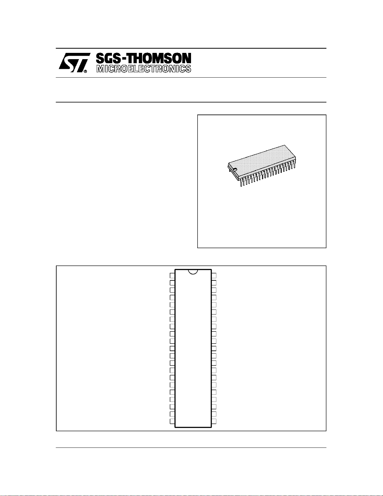
STV2102
PRELIMINARY DATA
DESCRIPTION
The STV2102isa PALchroma decoder,video and
H/V deflection processor forCTV.
Usedwith theTDA8222,this IC permitsacomplete
low cost solution with external output stages.
It is pin compatible with STV2110 PAL/SECAM
processor.
PINCONNECTIONS
VccSUPPLY VOLTAGE
1
BLKBLANKING INPUT
2
GREEN CUT-OFFCAPACITOR
HORIZONTAL Vcc
BLUE OUTPUT
BLUE CUT-OFF CAPACITOR
LUMINANCE SIGNAL INPUT
SCANNING LOOP FILTER
SCANNING XTAL
COMPOSITEVIDEO SIGNAL
LINE FLYBACKINPUT
VERTICAL OUTPUT
HORIZONTAL OUTPUT
CONTRASTCONTROL
GROUND GND
DELAY CHROMAINPUT
CHROMASTANDARD
COG
ROUTRED OUTPUT
HVcc
GOUTGREEN OUTPUT
BOUT
COB
YIN
SLPF
SXTL
CVBS
LFB
VOUT
HOUT
CTR
PALINPAL CHROMA INPUT
NCNOT CONNECTED
DLI
3
4
5
6
7
8
9
10
11
12
13
14
15
16
17
18
19
20
PS
21
(Plastic Package)
ORDER CODE : STV2102
ICAT CATHODE CURRENT
42
SUPPLY VOLTAGEINPUT
Vcc
41
BIN
40
39
38
37
36
35
34
33
32
31
30
29
28
27
26
25
24
23
22
BLUE INPUT
GIN GREEN INPUT
RED CUT-OFF CAPACITOR
COR
RIN RED INPUT
BRIGHTNESS CONTROL
BRIG
FAST BLANKINGINPUT
FBL
CHROMA LOOP FILTER
CLPF
CXTL
CHROMA XTAL
CKP
PAL KILLER CAPACITOR
NC NOT CONNECTED
ACC ACC CONTROL CAPACITOR
NC NOT CONNECTED
NC NOT CONNECTED
SAT
SATURATION CONTROL
NC NOT CONNECTED
NC NOT CONNECTED
GND GROUND
NC NOT CONNECTED
DLO
CHROMA OUTPUT
SHRINK 42
2102-01.EPS
May 1992
This isadvance information on anewproduct now in developmentor undergoingevaluation. Details are subject to changewithout notice.
1/12
Page 2

STV2102
BLOCK DIAGRAM
ROUT
4
GOUT
6
BOUT
7
COR
COG
3388
COB
ICAT
42
HOUT
BLK
2
VOUT
14
15
Line
Output
Counter
Output
Shift
Phase
Phase
Comp. 2
Blank.
Comp.
Blanking
Blk. RGB
36
BRIG
Brightness
RGB
Cut-off
Meas.
Leak. Current
Meas.
Tube Temp
Separator
FrameSync.
Decoder
Frame
Line
VCO
Divider
Phase
Comp. 1
Sep.
Sync.
11
SXTL
10
SLPF
12
CVBSPS LFB
16
13
40
RGB
Contrast
39
+ Clamp
Switch
PAL
Flip-Flop
Generator
Burst Gate
Mute
SAT
37
35
Matrix
Saturation
28
29
2/12
SAT FBL RIN GIN BIN CTR
Black
Insertion
5
HVccVcc Vcc
Y Input
Contrast
12741
YIN 9
Black
Reference
Clamp
PAL
XVCO
33CXTL
Demod.
90deg
Phase
Detector
34
CLPF
Killer
Burst
30
ACC
Detector
32
CKP
DL
ACC
18
PALIN
Matrix
17
NC
21 26
31
NC
23
NC
20
19
GND
24
GNDDLO DLI
22 25
2102-02.EPS
NC NC NC NC
Page 3

STV2102
FUNCTIONAL DESCRIPTION
DEFLECTION
SynchronizationSeparator
The synchronization separator is based on the
bottom of synchronizationpulses alignment to an
internal reference voltage. An external capacitor
permitsto alignsynchro.pulses,twoexternalresistorsdetermines the detection threshold ofsynchro
pulses. The frame synchronization pulses are
locked to a 32µs reference signal to perfect inter-
lacing.
HorizontalScanning
Thehorizontalscanningfrequencyisobtainedfrom
a 500kHzVCO. The circuit uses twophase-locked
loops (PLL). The first one controls the frequency;
the second one, fullyintegrated, controls the relative phase of the synchronizationand the line flyback signals.
The first PLLhas twotimesconstants: a long time
constant during the picture to have a good noise
immunity, a shorttime constantat thebeginningof
the frame to recapture faster the phasein case of
VCR video signal. More over,the PLL is in short
time constant three linesbefore frame pulses occured, it permits to ensure good interlacingwhen
the video signalcomesfrom aVCR tape with high
phaseerror.
The horizontal output signal is 28µs width. On
starting up, horizontal pulses are enabled at
V
= 6.8V. On shutting down, horizontal pulses
CC
areinhibited for V
CC
= 6.2V.
The vertical output signal is 10.5 lines width. It
permits to drive a sawtooth generator such as
TDA1771.
A video recognition function permits to sent the
informationof no video identificationto SATpin : it
forcesa lowlevel when no video detectionoccurs.
CHROMA
ACC Amplifier,DL Matrix and Demodulator
The correct chroma subcarrier input, issued from
bandpass,is internallyselected with the standard.
The ACC amplifier envolves three stages :the first
one select the correct input, the second one the
-6dB in picture (PAL mode), the third one is controledby theACC voltage.
The dynamic range is overthan 30dB.
The chrominanceoutput signalis fed to the delay
line.
The adding and substracting direct and delayed
signals are performed by the DL matrix function.
Two synchronous demodulators multiplies
the (B-Y)signalwith the 0 degree phase4.43MHz
referencesignaland the (R-Y) signalwiththealternate ±90 deg.4.43MHz phase referencesignal.
4.43MHz Phase Locked Loop
The oscillating frequency of the 4.43MHz crystal
oscillatoris controlledby the outputvoltage of the
loop filter.The phase detector will lock the 90 degree reference signal to the direct burst signal.
A 90 degree phase shifter permits to recover the
0 degreereferencesignal.Aflip-flop driven byline
pulses permits to generate the alternate ± 90degree signal.
ACC Control and Color Killer
Thedirectburstsignalisdemodulatedwiththe± 90
degree referencesignal. The demodulationresult
is usedby ACCcontrol and killer function.
If the demodulation result is always positive, the
killercapacitoris charged and thestandardis identified (color ON). When demodulation result is always negative, the killer capacitor voltagereaches
the flip-flop inhibition level, so the alternace sequence is reversed and the capacitor is charged
again.
In case of no video signal, the killer capacitor
voltage is maintained about V
/2, below thecolor
CC
off threshold.
VIDEO
The luminance input is controlled by the contrast
controlstage which range is 20dB.
The luminance and color difference signals are
added in the video matrix circuit toobtainthe color
signals.
The colorsignals are sent to anRGBswitchwhich
will drive to the outputs either internal RGB signals
or externalRGB signals.
Automatic Cut-off Control
The blacklevelsof the RGB outputsarecontrolled
with the cut-off loops duringthree line periodsafter
the frame retrace. The cut-off measurements are
sequentiallyachievedduringthese threelines.The
leakage current measurement is achieved during
the frame retrace and memorized on an internal
capacitor, thus the circuit is able to extract the
cut-offcurrentfromthe total currentmeasurement.
Warm-up Detector
At the start-up, the cut-off loops are switch off, a
white level is insertedon the luminance signal until
a cathode current is detected. Then the cut-off
loops are released.
3/12
Page 4
STV2102
RGB Inputs
To avoid the black level of the inserted signal
differing from the black level of the normal video
signal,the externalRGB are clamped to the black
level of the luminance signal. Therefore, an AC
couplingis required for the RGB inputs.
The RGB inputs are controlled by a 12dB range
contrast control stage.
ABSOLUTE MAXIMUM RATINGS
Symbol Parameter Value Unit
V
T
T
SupplyVoltage 12 V
cc
Storage Temperature -55, +150
stg
Operating Temperature 0, +70
oper
THERMALDATA
Symbol Parameter Value Unit
R
th (j-a)
DC AND ACELECTRICAL CHARACTERISTICS (VCC=9V,T
Symbol Parameter Test Conditions Min. Typ. Max. Unit
HV
V
I
I
ccv&c
LUMINANCE INPUT (Pin 9)
V
VDC9 DC Operating Voltage No inputsignal 2.5 V
CONTRAST CONTROL (Pin 16)
V
V
16 (Max.)
G
BRIGHTNESS CONTROL (Pin 36)
V
V
36 (Max.)
SATURATION CONTROL INPUT (Pin27)
V
V
29 (Max.)
G
RGB CLAMP CAPACITORS (Pins 4-7-39)
I
4-7-39
I
i4-7-39
RGB OUTPUTS (Pins 4-6-7)
V
BW 4-6-7
Junction-ambient Thermal Resistance Max. 70
=25oC unlessotherwise specified)
amb
Scanning Supply Voltage (Pin 5) 8.1 9 9.9 V
cc
Video& Chroma Supply Voltage(Pins 41-42) 8.1 9 9.9 V
cc
Scanning Supply Current(pin 5) No load 20 30 mA
cch
Video& Chroma Supply Current (Pins 41-42) No load 45 55 mA
P
TotalPower Dissipation No load 580 850 mW
D
InputLevel before Clipping (black to white) 350 mV
BW9
I
InputCurrent •During burst period
g
Luma Gain 5.5
G
9
Contrast Control Voltage 2 to 4 V
16
•Out of burst period
±100
Maximum Allowed Control Voltage 5 V
Contrast Control Range 20 dB
16
I
InputCurrent 10 µA
16
Brightness Control Voltage 1.5 to 4.5 V
36
Maximum Allowed Control Voltage 5 V
I
InputCurrent 10 µA
36
InputCurrent 10 µA
I
29
Saturation Control Voltage 2 to 4 V
29
Maximum Allowed Control Voltage 5 V
Saturation Control Range -50 dB
29
ControlCurrent ±150 µA
Leakage Current 1 µA
Output Signal Amplitude (black to white) •0.35V B to W @Pin9
2V
•Contrast @ max
•Sat. & Brig. @ 3V
5
o
C/W
o
o
µA
µA
C
C
2102-01.TBL
2102-02.TBL
PP
2102-03.TBL
4/12
Page 5

STV2102
DC ANDAC ELECTRICAL CHARACTERISTICS (continued)
=9V,T
(V
CC
Symbol Parameter Test Conditions Min. Typ. Max. Unit
RGB OUTPUTS (Pins 4-6-7) (continued)
-I
4-6-7
VM
4-6-7
V
blank4-6-7
∆V
temp
BW
4-6-7
RGB INPUTS (Pins 37-39-40)
V
BW37-39-40
V
clamp
37-39-40
BW
37-39-40
G
CTR
G
37-39-40
FAST BLANKING INPUT (Pin 35)
V
TH1-35
V
TH2-35
I
35
T
switch
T
blank
CATHODE CURRENT INPUT (Pin 42)
AUTOMATIC CUT-OFF (Pin3-8-38)
V
4-6-7
CHROMINANCE INPUT (Pin 18)
V
18
V
burst-18
G
ACC
R
18
V
DC-18
ACC CAPACITOR (Pin 30)
I
30
I
i30
PLL LOOP FILTER (Pin 34)
I
34
I
i34
CHROMAXTAL (Pin 33)
CR
33
=25oC unless otherwisespecified)
amb
Individual Output Sinking Current 2 mA
Maximum Peak White Level 7.8 V
Blanking Level 0.7 V
Relative Variation in Black Levelwith Various
20 mV
CONT. SAT. BRIG between the 3 channels
Black Level Thermal Drift 0.5 mV/oC
Bandwith - 3dB 5 MHz
Tracking between Luminance and Chrominance
2dB
Signals over 10dBContrast Control
Maximum Input Level (B to W) 2 V
Clamp Level Contrast max 1.5 V
Bandwidth -3dB 8 MHz
RGB Contrast Control Range 12 dB
RGB Gain 4
First Threshold (switching) 0.7 V
SecondThreshold (switching) 2.1 V
InputCurrent 0V @Pin 35 50 µA
Switching Delay 50 ns
Blanking Delay 50 ns
Leakage Current Reference Voltage 1.75 V
CO Reference refered to Leakage Current
250 mV
Reference
Low Voltage Output Current 200 µA
Capacitor Cut-off Positive Negative Clamping 100 µA
Start-beam Current Detection Reference
2V
Voltage
Cut-off Output Range 3 V
InputLevel BeforeClipping 900 mV
Minimum Burst Signal Amplitude within the
30 mV
ACC Control Range
ACC Control Range Change of burst over whole
30 dB
ACC ControlRange < 1dB
InputImpedance 8 kΩ
DC Operating Voltage No input signal 3.5 V
Charging Current During burst gate period 250 µA
Leakage Current Out of burst gate period 1 µA
ControlCurrent 400 µA
Leakage Current 5 µA
Catching Range 700 Hz
PP
PP
2102-04.TBL
5/12
Page 6

STV2102
DC AND AC ELECTRICAL CHARACTERISTICS (continued)
=9V,T
(V
CC
Symbol Parameter Test Conditions Min. Typ. Max. Unit
SUBCARRIER OUTPUT (Pin22)
V
burst-22
KILLER CAPACITOR (Pin 32)
V
OFF-32
V
ON-32
V
INH-32
I
32
I
i32
V
nom-32
DELAYED CHANNEL INPUT (Pin 20)
V
DC-20
R
20
COMPOSITE VIDEO BASE BAND SIGNAL (Pin 12)
V
REF-12
V
12
SCANNING XTAL (Pin 11)
F
11
CR
11
PLL LOOP FILTER (Pin 10)
I
iow-10
I
high-10
DELAYED LINE FLYBACK INPUT (Pin 13)
V
TH-13
V
13
V
DC-13
I
13
DIRECT BLANKING INPUT (Pin2)
V
TH-2
V
2
V
DC-2
I
2
Ph2
2
HORIZONTAL OUTPUT (Pin15)
T
15
V
low-15
V
start-15
V
stop-15
∆t
15
VERTICAL OUTPUT (Pin 14)
T
14
T
sync
V
low-14
=25oC unless otherwisespecified)
amb
Output Burst Amplitude (PAL mode) Within ACC Control Range 2.2 Vpp
Collor offVoltage No chroma signal 4.9 V
Color on Voltage 5.4 V
PAL Flip-flopInhibition Level 3.2 V
Control Current 250 µA
Leakage Current 5 µA
Voltage withNominal Input Signal 6.0 V
DC Operating Voltage No input Signal 2.2 V
Input Impedance PAL standard 8 kΩ
Voltage Reference I12=-1µA 0.6 0.8 1.0 V
Video InputSignal 2.5 V
Frequency afterDivider 15.625 kHz
Frequency ControlRange after Divider ±700 Hz
Low Loop Gain Output Current 0.15 mA
High Loop Gain Output Current 0.40 mA
Window Pulse Width 4 µs
Threshold 0.6 V
Line Flyback Amplitude 1.5 V
Minimum Negative Voltage -0.4 V
Input Current 5 µA
Threshold 0.6 V
Line Flyback Amplitude 1.5 Vpp
Minimum Negative Voltage -0.4 V
Input Current 5 µA
External Adjustment Appli. Adjust. 2 4 6 µs
Output Pulse Width 26 28 29 µs
Output Voltage(open collector) I15= 10mA 1 V
Vcc Start Level 6.8 V
Vcc Stop Level 6.2 V
ϕ2 Phase Range 10 µs
Output Pulse Width 10.5 lines
Frame Synchro. Window 248to
352
Output Voltage(Open collector) 1 V
PP
PP
line
2102-05.TBL
6/12
Page 7

Figure1 : Pins 3-8-38-42(COG, COB, COR, ICAT)
42
Figure2 : Pins 37-39-40(RIN, GIN,BIN)
STV2102
3-8-38
2102-03.EPS
Figure3 : Pins 4-6-7 (ROUT, GOUT,BOUT)
37-39-40
Figure4 : Pin 9 (YIN)
4-6-7
2102-04.EPS
2102-05.EPS
Figure5 : Pin 10 (SLPF)
10
9
2102-06.EPS
2102-07.EPS
7/12
Page 8

STV2102
Figure6 : Pin 11(SXTL)
Figure8 : Pins 2-13 (BLK, LFB)
2-13
Figure7 : Pin 12 (CVBS)
V
REF
11
2102-08.EPS
12
2102-09.EPS
Figure9 : Pins 14-15 (VOUT, HOUT)
14
15
Figure 10 : Pins16-27(CTR, SAT)
16
2102-10.EPS
Figure13 : Pin 18 (PALIN)
V
REF2
V
REF
2102-12.EPS
2102-11.EPS
18
2102-13.EPS
8/12
Page 9

STV2102
Figure11 : Pin 20 (DLI)
20
V
REF1
Figure14 : Pin 32 (CKP)
Figure12 : Pin 21 (PS)
21
2102-14.EPS
Figure15 : Pin 22(DLO)
2102-15.EPS
32
2102-16.EPS
22
2102-17.EPS
9/12
Page 10

STV2102
Figure16 : Pin 30 (ACC)
Figure 17 : Pin36 (BRIG)
30
2102-18.EPS
Figure18 : Pin 33(CXTL)
36
Figure19 : Pin 34 (CLPF)
Base Current
Compensation
34
Phase
Comparator
33
2102-19.EPS
Figure20 : Pin 35 (FBL)
35
2102-20.EPS
10/12
2102-21.EPS
2102-22.EPS
Page 11

APPLICATIONDIAGRAM
22kΩ
39kΩ
Vcc
Vcc
Vcc
HVcc
SAT
39kΩ
39kΩ
ICAT
BIN
RIN GIN
FBL
22nF100
F
µ
100nF
15kΩ
BRIG
CTR
Vcc
22kΩ
47kΩ
100nF 100nF 22kΩ
100nF
75Ω
75Ω
Ω
75
75Ω
22nF100µF
MUTE
15kΩ
15kΩ
22nF
22nF
22nF
BRIG
CTR
ICAT
COB
COR COG
BIN
GIN
RIN
FBL
HVcc
Vcc
36
16
42
8
38 3
40
37
35 39
5
41
1
10nF
DL
1kΩ
SAT
YIN
27
9
&
CVBS
TRAP
ROUT
GOUT
Ω
470Ω470Ω470
6
4
33
CXTL
4.43MHz
1kΩ
CC
V
BOUT
7
470kΩ
Ω
10k
CC
V
34
CLPF
VERTICAL
DEFLECTION
(TDA1771)
RAMP GENERATOR
VOUT
1kΩ min.
30
ACC
33nF
6.8nF
3.3nF 680kΩ
47nF
+V
1kΩ min.
CC
V
14
STV2102
32
23
CKP
CKS
6.8nF
10nF
1kΩ
390Ω
HOUT
18
PALIN
CVBS
STV2102
V1
V2
LINE
YOKE
Ω
1k
500kHz
47nF
SXTL
15
11
21
Vcc
H
µ
10
120pF
EHT
µF
1
TRANSFORMER
3.9kΩ
10nF
3kΩ
100pF
2.2µF
CVBS
SLPF
500kΩ
10
12
BLK
13
LFB
CVBS
LBF
5.6kΩ
1kΩ
4.7nF
19 2
GND
2420
GND
330Ω
10nF
1kΩ
390Ω
DL
10µH10µH
Ω
DLI
10nF
22
PS
DLO
750
2102-22.EPS
11/12
Page 12

STV2102
PACKAGE MECHANICAL DATA
42 PINS- PLASTICSHRINK DIP
e4
F
A
I
a1
L
b1
e
Stand-off
22
21
E
Dimensions
b2
b
e3
D
42
1
Millimeters Inches
Min. Typ. Max. Min. Typ. Max.
A 3.30 0.130
a1 0.51 0.020
b 0.35 0.59 0.014 0.023
b1 0.20 0.36 0.008 0.014
b2 0.75 1.42 0.030 0.056
b3 0.75 0.030
D 39.12 1.540
E 15.57 17.35 0.613 0.683
e 1.778 0.070
e3 35.56 1.400
e4 15.24 0.600
F 14.48 0.570
i 5.08 0.200
L 2.54 0.100
PMSDIP42.EPS
SDIP42.TBL
Information furnished is believed tobe accurate andreliable. However, SGS-THOMSON Microelectronics assumes no responsibility
for the consequences of use of suchinformation norfor any infringement of patentsor otherrights of third parties which may result
from its use. No licence is granted by implication or otherwiseunder anypatent or patent rights of SGS-THOMSON Microelectronics.
Specifications mentioned in this publication are subject to change without notice. This publication supersedes and replaces all
information previously supplied.SGS-THOMSON Microelectronics products are not authorized for use as critical componentsin life
support devices or systems without express written approval of SGS-THOMSON Microelectronics.
1994 SGS-THOMSON Microelectronics - All Rights Reserved
Purchase of I
2
I
C Patent. Rights to usethese components in a I2C system,is granted provided that thesystem conforms to
2
C Componentsof SGS-THOMSON Microelectronics,conveys a license under the Philips
2
the I
C Standard Specificationsas defined by Philips.
SGS-THOMSON Microelectronics GROUP OF COMPANIES
Australia - Brazil -China - France - Germany - Hong Kong -Italy -Japan - Korea- Malaysia - Malta - Morocco
The Netherlands - Singapore -Spain - Sweden - Switzerland - Taiwan - Thailand - United Kingdom - U.S.A.
12/12
 Loading...