

Page 1
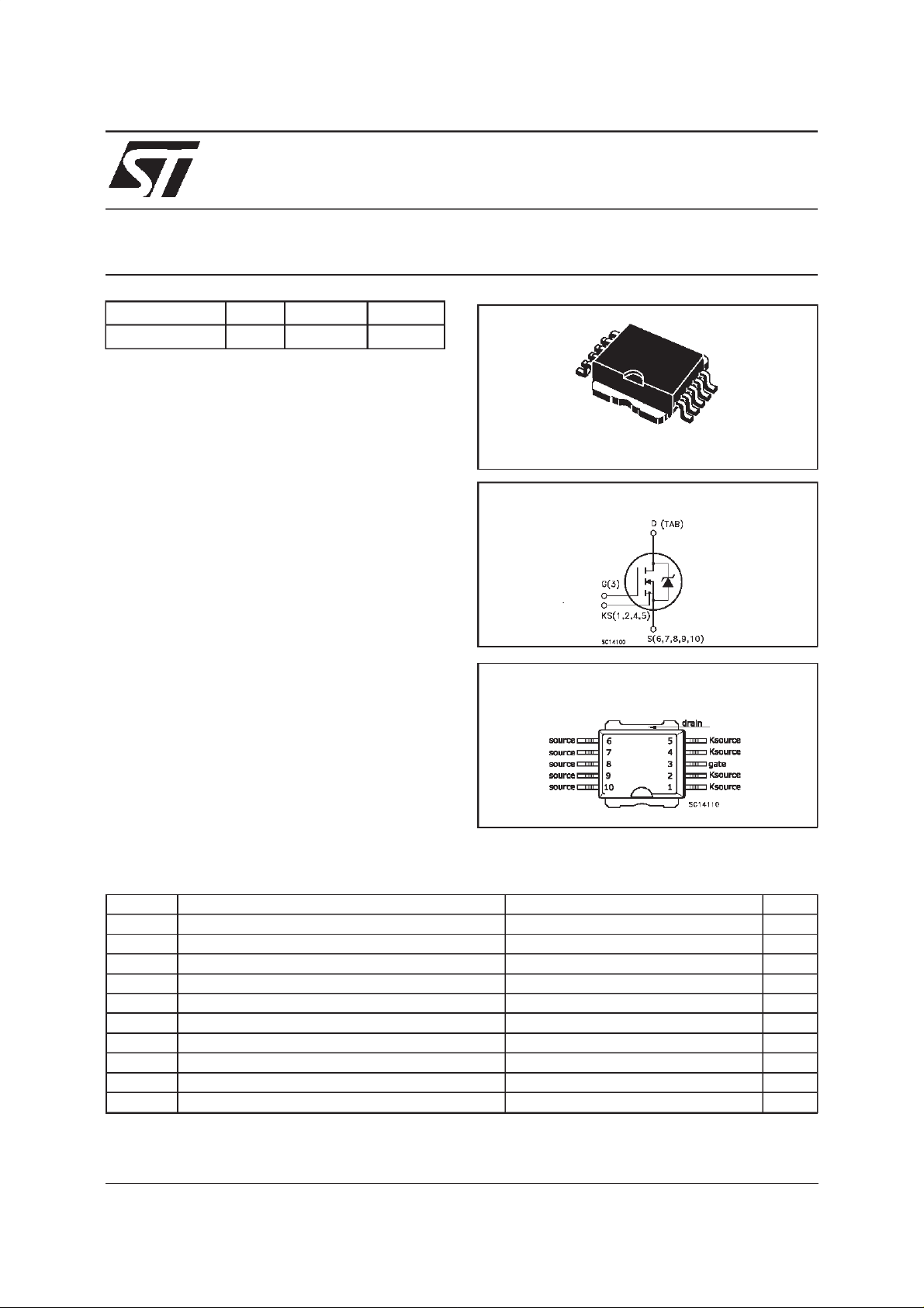
STV160NF02L
N - CHANNEL 20V - 0.0016Ω - 160A - PowerSO-10
STripFET MOSFET
TYPE V
DSS
R
DS(on)
I
D
ST V160NF02L 20 V < 0.0025 Ω 160 A
■ TYPICALR
■ ULTRA LOW ON-RESISTANCE
■ ULTRA FAST SWITCHING
■ 100%AVALANCHETESTED
■ VERYLOW GATE CHARGE
■ LOW THRESHOLDDRIVE
■ LOW PROFILE, VERY LOWPARASITIC
DS(on)
= 0.0016 Ω
INDUCTANCE PowerSO-10PACKAGE
DESCRIPTION
The STV160NF02L represents the second
generation of Application Specific
STMicroelectronics well established STripFET
process based on a very unique strip layout
design. The resulting MOSFET shows unrivalled
high packing density with ultra low on-resistance
and superior switching charactestics. Process
simplification also translates into improved
manufacturing reproducibility. This device is
particularly suitable for high current, low voltage
switchingapplicationwhere efficiency is crucial.
10
1
PowerSO-10
INTERNAL SCHEMATIC DIAGRAM
CONNECTIONDIAGRAM (TOP VIEW)
APPLICATIONS
■ BUCK CONVERTERSIN HIGH
PERFORMACETELECOMAND VRMs
DC-DC CONVERTERS
ABSOLUTE MAXIMUM RATINGS
Symbol Parameter Value Uni t
V
V
V
I
D
I
DM
P
T
(•) Pulse width limited by safe operating area (**) Limited only maximumjunction temperature allowed by PowerSO-10
June 1999
Drain-source Voltage (VGS=0) 20 V
DS
Drain- gate Voltage (RGS=20kΩ)20V
DGR
Gate - source V o lt age
GS
20 V
±
(**) Drain Current (cont inu ous) at Tc=25oC 160 A
I
Drain Current (cont inu ous) at Tc=100oC 113 A
D
(•) Drain Current (pulsed) 640 A
Tota l Dissipati on at Tc=25oC 160 W
tot
Derat ing F ac t or 1.07 W/
Stor age Tem perature -65 to 175
stg
Max. Operating Junct ion Tem perature 175
T
j
o
C
o
C
o
C
1/8
Page 2
STV160NF02L
THERMAL DATA
R
thj-case
R
thj-amb
T
Ther mal Resistance J unction- cas e Max
Ther mal Resistance J unction- ambient Max
Maximum Lead Temperatu re F or So lder ing Purpos e
l
0.9375
50
300
o
C/W
o
C/W
o
C
ELECTRICAL CHARACTERISTICS
=25oC unlessotherwisespecified)
(T
J
OFF
Symbol Parameter Test Conditions Min. Typ. M ax. Unit
V
(BR)DSS
Drain-source
ID=250µAVGS=0 20 V
Break dow n Volt age
I
DSS
I
GSS
Zero Gate Voltage
Drain Cur rent ( V
GS
Gat e- bod y L eak ag e
Current (V
DS
=0)
=0)
V
=MaxRating
DS
=MaxRating Tc=25oC
V
DS
V
=± 15 V
GS
1
10
100 nA
±
ON(∗)
Symbol Parameter Test Conditions Min. Typ. Max. U nit
V
GS(th)
R
DS(on)
I
D(on)
Gate Threshold Voltage VDS=VGSID= 250 µATc=25oC11.72.5V
Sta t ic Drain -s ource On
Resistance
VGS=10V ID=80A
=8V ID=80A
V
GS
V
=4.5V ID=40A
GS
=10V ID=80A Tj=175oC
V
GS
V
=8V ID=80A Tj=175oC
GS
=4.5V ID=40A Tj= 175oC
V
GS
On State Drain Current VDS>I
D(on)xRDS(on )max
1.6
1.7
3.5
160 A
2.5
3.5
6
5.7
7
11.4
VGS=10V
µA
µA
m
mΩ
m
mΩ
m
mΩ
Ω
Ω
Ω
DYNAMIC
Symbol Parameter Test Conditions Min. Typ. Max. U nit
gfs(∗)Forward
Tr ansc on duc tance
R
C
C
C
Gate re sistance VDS=15V f=1MHz VGS=0 0.9 Ω
g
Input Capac i t ance
iss
Out put Capacitanc e
oss
Reverse Tr ansfer
rss
Capacit a nc e
C
C
C
Input Capac i t ance
iss
Out put Capacitanc e
oss
Reverse Tr ansfer
rss
Capacit a nc e
2/8
VDS>I
D(on)xRDS(on )maxID
= 80 A 210 S
VDS=15V f=1MHz VGS= 0 4900
2950
565
VDS=0V f=1MHz VGS= 0 7200
13000
4220
pF
pF
pF
pF
pF
pF
Page 3

STV160NF02L
ELECTRICAL CHARACTERISTICS
(continued)
SWITCHING ON
Symbol Parameter Test Conditions Min. Typ. Max. U nit
t
d(on)
Tur n-on Delay Time
Rise Ti m e
t
r
VDD=15V ID=40A
R
=4.7
G
Ω
VGS=10V
23
350
(Resis t iv e Loa d, see fig. 3)
Q
Q
Q
Tot al Gat e Charge
g
Gat e- Source Charg e
gs
Gate-Drain Charge
gd
VDD=16V ID= 160 A VGS= 10 V 103
38
9
SWITCHING OFF
Symbol Parameter Test Conditions Min. Typ. Max. U nit
t
d(off)
Tur n-of f D ela y Time
t
Fall T ime
f
VDD=15V ID=40A
R
G
=4.7
Ω
VGS=10V
105
120
(Resis t iv e Loa d, see fig. 3)
t
d(off)
t
r(Voff)
t
t
Tur n-of f D ela y Time
Off-volt ag e Rise T ime
Fall T ime
f
Cross-over T im e
c
V
=16V ID=80A
clamp
R
=4.7
G
Ω
VGS=10V
(Indu ct iv e Load , see f ig . 5)
85
46
335
404
SOURCEDRAINDIODE
Symbol Parameter Test Conditions Min. Typ. Max. U nit
I
SD
I
SDM
V
SD
t
Q
I
RRM
(∗) Pulsed:Pulse duration= 300 µs, duty cycle 1.5%
(•) Pulse width limited by safe operating area
Source-drain Current
(•)
Source-drain Current
160
640
(pulsed)
(∗)ForwardOnVoltage ISD= 160 A VGS=0 1.5 V
Reverse Recovery
rr
Time
Reverse Recovery
rr
ISD= 80 A di/dt = 10 0 A/µs
=15V
V
DD
(see test circuit, fig. 5)
100
0.25
Charge
Reverse Recovery
5
Current
ns
ns
nC
nC
nC
ns
ns
ns
ns
ns
ns
A
A
ns
µ
A
C
SafeOperating Area ThermalImpedance
3/8
Page 4
STV160NF02L
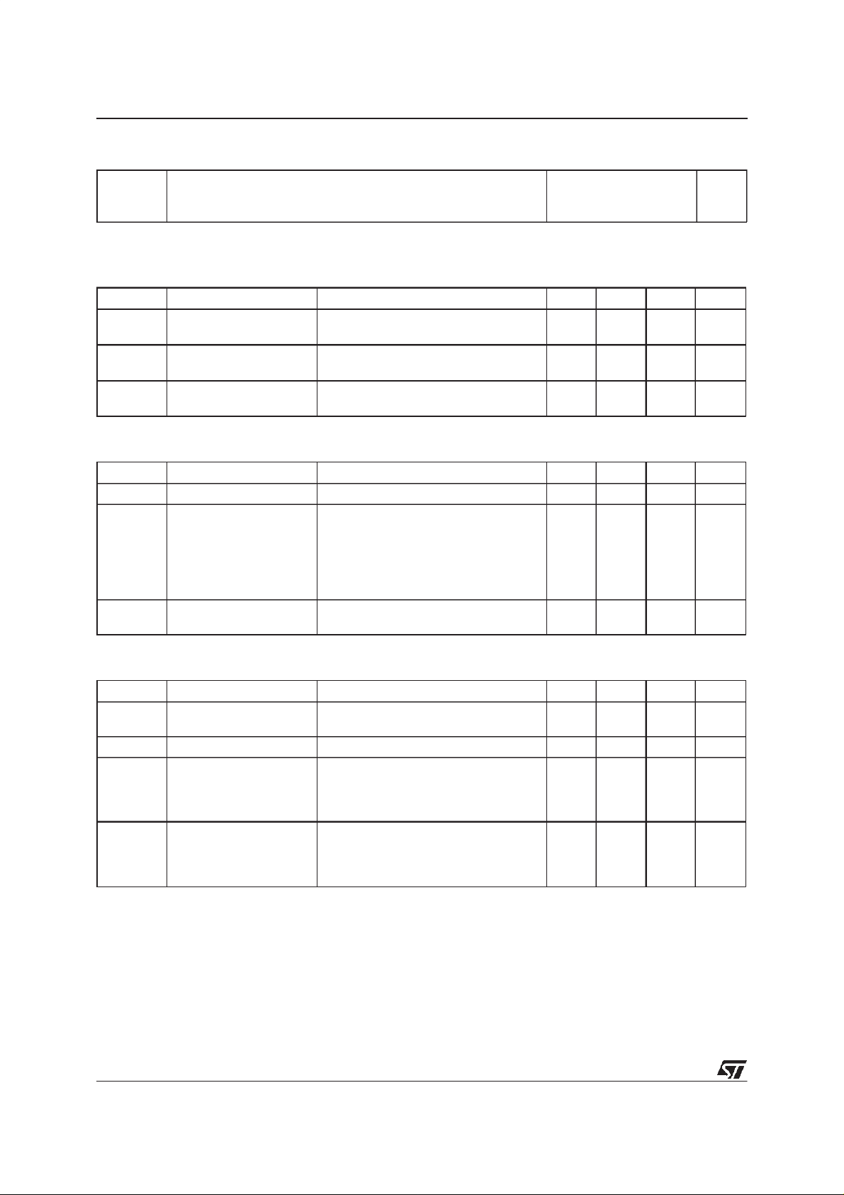
OutputCharacteristics
Transconductance
TransferCharacteristics
Static Drain-sourceOn Resistance
Gate Charge vs Gate-sourceVoltage
4/8
CapacitanceVariations
Page 5

STV160NF02L
NormalizedGate ThresholdVoltage vs
Temperature
Source-drainDiode Forward Characteristics
NormalizedOn Resistancevs Temperature
BasicSchematic For MotherboardVRM Whith
SynchronousRectification
BasicSchematic Mosfet Switch Used In
SecondarySideOf a FowardConvert
5/8
Page 6

STV160NF02L
Fig. 1
: UnclampedInductiveLoadTest Circuit
Fig. 3: SwitchingTimes Test Circuits For
ResistiveLoad
Fig. 2
: UnclampedInductive Waveform
Fig. 4: Gate Charge test Circuit
Fig. 5
: TestCircuit For Inductive Load Switching
And Diode Recovery Times
6/8
Page 7
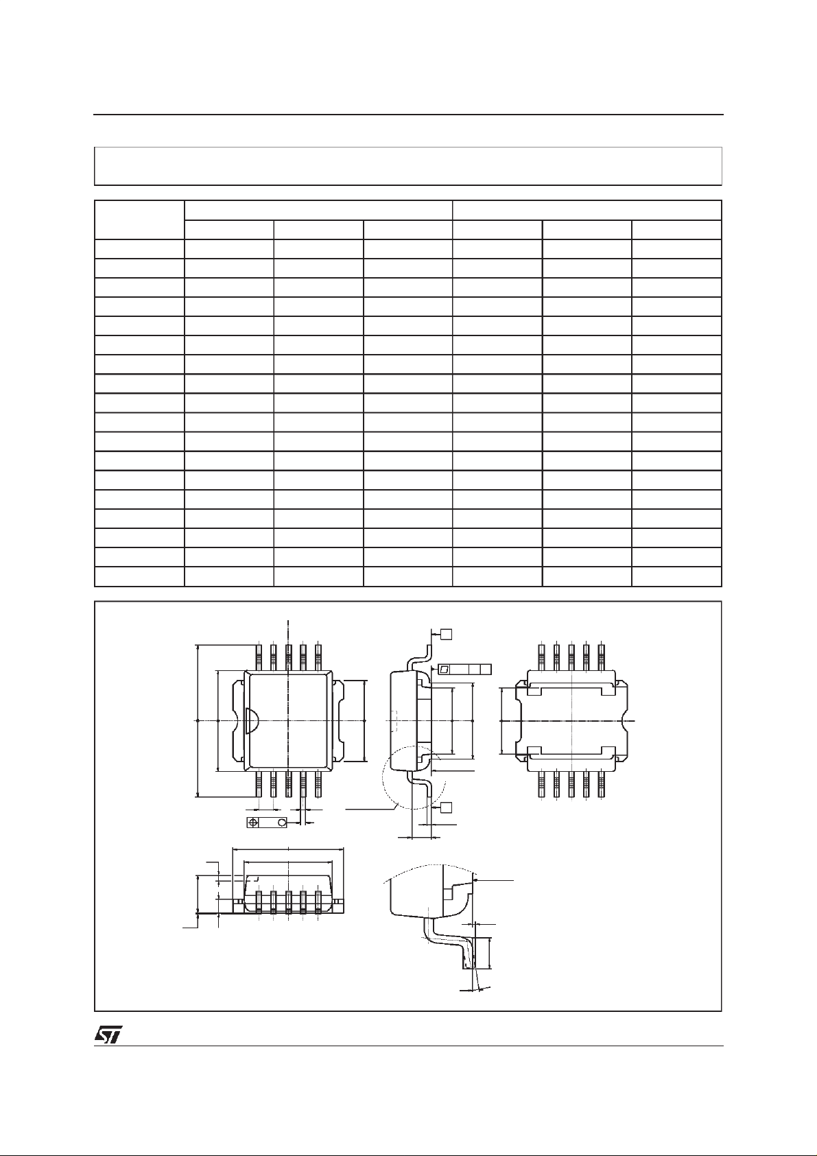
PowerSO-10 MECHANICAL DATA
STV160NF02L
DIM.
mm inch
MIN. TYP. MAX. MIN. TYP. MAX.
A 3.35 3.65 0.132 0.144
A1 0.00 0.10 0.000 0.004
B 0.40 0.60 0.016 0.024
c 0.35 0.55 0.013 0.022
D 9.40 9.60 0.370 0.378
D1 7.40 7.60 0.291 0.300
E 9.30 9.50 0.366 0.374
E1 7.20 7.40 0.283 0.291
E2 7.20 7.60 0.283 0.300
E3 6.10 6.35 0.240 0.250
E4 5.90 6.10 0.232 0.240
e 1.27 0.050
F 1.25 1.35 0.049 0.053
H 13.80 14.40 0.543 0.567
h 0.50 0.002
L 1.20 1.80 0.047 0.071
q 1.70 0.067
α 0
o
o
8
==
==
HE
h
A
F
A1
610
51
eB
M
0.25
D
==
D1
==
DETAIL”A”
E2
==
DETAIL”A”
Q
B
0.10 A
E1E3
==
SEATING
PLANE
A
C
α
B
E4
==
SEATING
PLANE
A1
L
==
0068039-C
7/8
Page 8
STV160NF02L
Information furnishedis believed tobeaccurate and reliable.However, STMicroelectronics assumes no responsibilityfor the consequences
of use of such information nor for any infringement of patents or other rights of third parties which may result from its use. No license is
granted by implication or otherwise under any patent or patent rights of STMicroelectronics. Specificationmentioned in this publication are
subjecttochange without notice. Thispublication supersedes and replaces all information previouslysupplied. STMicroelectronics products
are not authorized for use as critical components in lifesupport devicesor systemswithout express written approval of STMicroelectronics.
The STlogo is a trademark of STMicroelectronics
1999 STMicroelectronics – Printed in Italy – All Rights Reserved
STMicroelectronics GROUP OF COMPANIES
Australia - Brazil - Canada -China - France - Germany - Italy - Japan- Korea- Malaysia - Malta - Mexico - Morocco - The Netherlands -
8/8
Singapore - Spain - Sweden - Switzerland - Taiwan - Thailand - United Kingdom - U.S.A.
http://www.st.com
.
 Loading...