

Page 1
SERIALINTERFACE TRANSMISSION DECODER
BUILT-IN AUTOMATICEQUALIZER FOR UP TO
30dB ATTENUATION AT 135MHz (TYPICALLY
300m OF HIGH-GRADE COAXIAL CABLE), PLL
CIRCUITFORRECLOCKING,ANDSERIAL-PARALLELCONVERSIONCIRCUIT.
THIS SERIAL TRANSMISSION DECODER REQUIRESONLYFEWEXTERNALCOMPONENTS.
OTHERRELATEDIC’s INCLUDE:
.
STV1601A, A SERIAL TRANSMISSION ENCODER (PARALLEL-TO-SERIAL CONVERSION)
.
STV1389AQCOAXIALCABLE DRIVER
STV1602A
STRUCTURE
.
Hybrid IC
APPLICATIONS
SERIALDATA TRANSMISSION DECODER
.
100 to 270Mb/s
APPLICATIONSEXAMPLES
.
Serial data transmission of digital television
signals525-625 lines
.
4:2:2 component 270Mb/s(10-bit)
.
4*fscPALcomposite 177Mb/s (10-bit)
.
4*fscNTSC Composite 143Mb/s (10-bit)
FUNCTIONS
.
Cableequalizer
(maximumgain : 30dB at 135MHz)
.
PLL for serial clockgeneration
.
Reclocked repeater output (active loop
through)
.
Descrambler: modulo-2multiplicationby
G(x) = (x
.
Parallel-to-serial conversion
.
Syncmonitor output
.
Eye pattern monitoring
.
Input signal detector
DESCRIPTION
The STV1602Ais a Hybrid IC decoder which convertsserial data comingfroma serialtransmission
line into parallel data.
9+x4
+1)(x+1)
(Ceramic Package)
ORDER CODE : STV1602A
PIN CONNECTIONS
GND
AIX
27 26 25 24 23 22 21 20 19
CX
DIX
DIY
FV
28
29
30
31
32
33
34
35
ESI
36
37
123456789
ESO
GND
QFS
GND
MON
ADS
DPR
PGA37
AIY
SY
GND
SX
EE
V
QSW
RSE
TN1
EVR
EEVEE
V
SYN
PCK
18
17
16
15
14
13
12
11
10
D9
D0
D1
D2
D3
D4
D5
D6
D7
D8
1601A-01.EPS
December 1992
1/22
Page 2
STV1602A
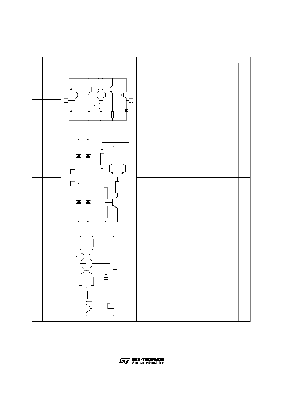
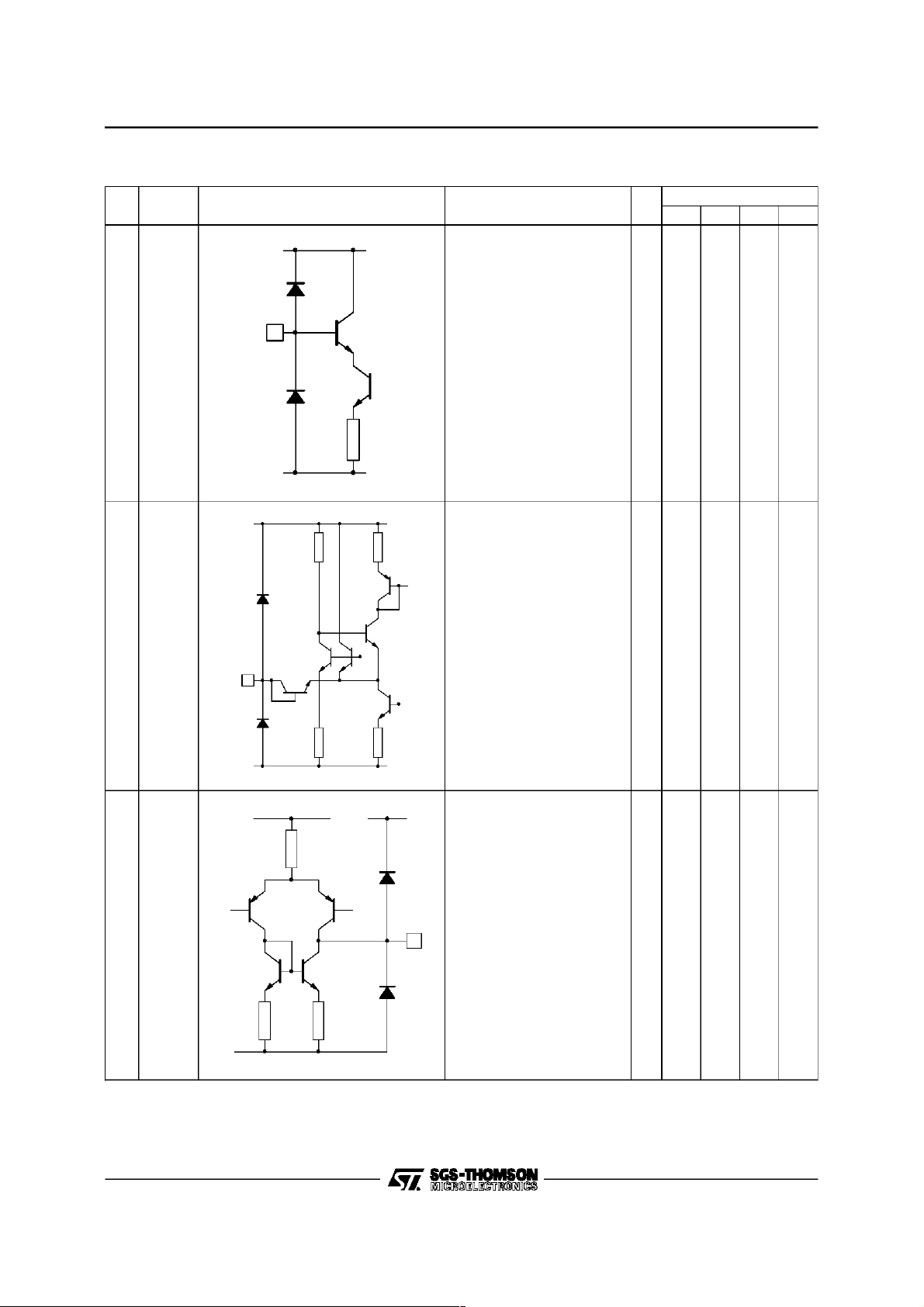
PIN DESCRIPTION
Pin
Symbol Equivalent Circuit Description I/O
o
N
GND
3SY
4SX
QSW
5
(GND)
30Ω 30Ω
34
V
R3
2kΩ 2kΩ
145Ω
V
EE
GND
1kΩ
36
Reclocked serial data output
in differential mode.
SX and SY are disabled
when TN1 is setHigh.
In this case, SX isset High
and SY is set Low
H
L
1602A-02.EPS
To be connected to GND I
Standard
Min. Typ. Max. Unit
O
-1.6
-2.4
V
V
36 FV
1 ESO
5
V
EE
1kΩ 1kΩ
2kΩ
10kΩ
10kΩ
2kΩ
GND
1
V
Adjustment of VCO Free
running frequency : V
gives the lowest frequency.
EE
level
I
To adjust it, set TN1 High.
1602A-03.EPS
Output of phase comparator
O -3.2 V
: must be connected to ESI
with the shortest distance
EE
1602A-04.EPS
1602A-01.TBL
2/22
Page 3
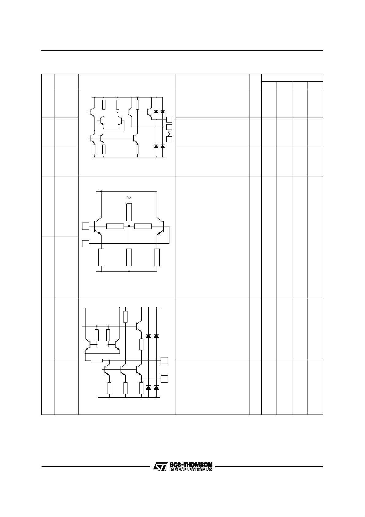
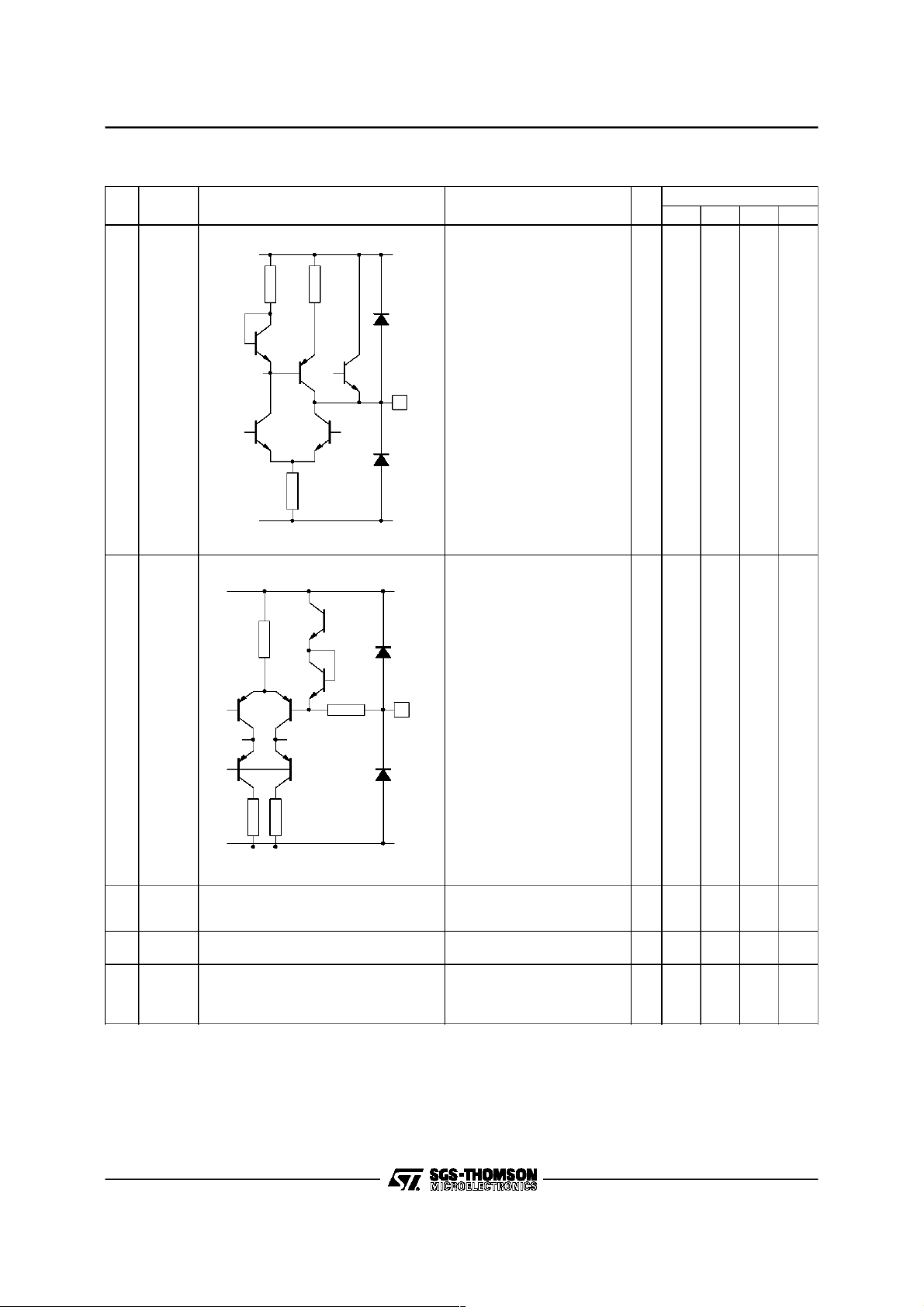
PIN DESCRIPTION(continued)
Pin
Symbol Equivalent Circuit Description I/O
o
N
STV1602A
Standard
Min. Typ. Max. Unit
9
D9
to
18
to
D0
19 PCK
21 EVR
26 AIX
25 AIY
GND
V
R3
V
GND
26
25
V
EE
EE
600Ω 600Ω 300Ω
210Ω 210Ω
300
Ω
10kΩ 10kΩ
3kΩ 4kΩ4kΩ
Parallel data output
H
L
21
Parallel clock output (rising
9
edge at data center)
18
H
L
Data output reference
O
-0.8
-1.6
O
-0.8
-1.6
O -1.2 V
potential
1602A-05.EPS
Equalizer differential input I -2.0 V
V
V
V
V
1602A-06.EPS
GND
2kΩ
28 NC To beleft open I -4.6 V
1kΩ
29
28
29 CX
16kΩ 2kΩ 2kΩ
Equalizer detectoroutput;
Input signal :
V
EE
1602A-07.EPS
absent
present
O
-2.4
-2.0
V
V
1602A-02.TBL
3/22
Page 4
STV1602A
PIN DESCRIPTION(continued)
Pin
Symbol Equivalent Circuit Description I/O
o
N
GND
1kΩ
31
Equalizer monitoroutput.
Connect 75Ω resistor
between MON-GND.
Observe using a 50Ω input
oscilloscope at the 75Ω
coaxial cable.
1602A-08.EPS
31 MON
V
GND
500Ω
R3
500Ω500Ω
V
EE
Standard
Min. Typ. Max. Unit
O
15 mV
(pp)
32 ADS
33 DIX
34 DIY
V
GND
33
34
V
EE
2kΩ2kΩ
32
?
V
R2
Serial data input selection
High : Digital input DIX/DIY
I
Low :Equalizer input
V
R3
2k
Ω
EE
500Ω 500Ω
1602A-09.EPS
L
Serial data digital differential
H
V
R1
V
R3
input
Selected when ADS is High.
H
L
500Ω
1602A-10.EPS
-0.5
-5VV
I
-1.0
-1.6VV
1602A-03.TBL
4/22
Page 5
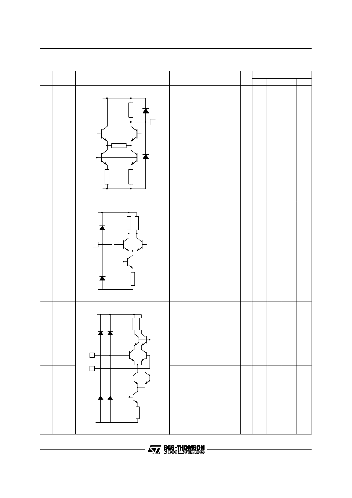
PIN DESCRIPTION(continued)
Pin
Symbol Equivalent Circuit Description I/O
o
N
GND
STV1602A
Standard
Min. Typ. Max. Unit
37 ESI
6TN1
GND
V
37
PLL error signalinput : must
i
be connected to ESO with
the shortest distance
2kΩ
V
EE
20kΩ
2kΩ
1602A-11.EPS
Serial data input activation
I
High : Input disabled (VCO
-3.2 V
-1.0
free running condition).
Low :Input enabled.
-4.0VV
During switch-on phase, by
6
4kΩ12kΩ
EE
temporarily hold High for
quick start-up
1602A-12.EPS
20 SYN
GND
4kΩ
V
CC
State changesat each TRS
O
Sync word
3FFH 000H 000H
20
2kΩ
V
EE
2kΩ
1602A-13.EPS
H
L
-1.0
-4.0VV
1602A-04.TBL
5/22
Page 6
STV1602A
PIN DESCRIPTION(continued)
Pin
Symbol Equivalent Circuit Description I/O
o
N
GND
1kΩ 1kΩ
Standard
Min. Typ. Max. Unit
35 DPR
22 RSE
Serial data detection output.
O
When there is an input
signal at theinput side
selected through ADS, this
pin goes High.
At no signal, it goes Low.
35
H
L
-1.0
-4.0VV
i.e.
- present : High
- absent : Low
6kΩ
V
EE
2kΩ
10kΩ
GND
22
1602A-14.EPS
Selects VCO frequency
range
H : High range
140 to 270MHz
I
L : Low range
100 to 145MHz
H
L
-0.4
-4.0VV
7
V
23
8V
2
24
GND GND
27
30
6/22
EE
EE
10kΩ10kΩ
V
EE
1602A-15.EPS
-5V supply
I/O buffer, PLL
-5.2 -5.0 -4.8 V
equalizer
-5V Supply
Logic part
-5.2 -5.0 -4.8 V
1602A-05.TBL
Page 7
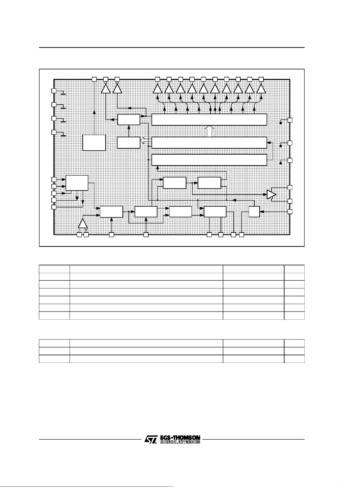
BLOCK DIAGRAM
STV1602A
GND
GND
GND
GND
AIX
AIY
QFS
CX
MON
EVR SYN PCK
21 20 19
2
INPUT
SELECT
Parallel clock
TIMING
GENERATOR
SYNC
DETECTOR
24
27
30
AUTOMATIC
26
25
EQUALIZER
28
29
31
ECL OUT
REFERENCE
VOLTAGE
CABLE
33 34 371363532 6
DIX DIY ADS TN1 DPR FV ESO ESI
D0 D1 D2 D3 D4 D5 D6 D7 D8 D9
18 17 16 15 14 13 12 11 10 9
10-BITLATCH
30-BIT SHIFT REGISTER
94
X + X + 1 DESCRAMBLER
DATA
RELAY
DATA
DETECTOR
Serial clock
EDGE
DETECTOR
NRZI TO NRZ
PHASE
DETECTOR
Reclocked serial data
VCO
V
7
EE
V
23
EE
V
8
EE
4
SX
3
SY
22
RSE
1602A-16.EPS
ABSOLUTEMAXIMUMRATINGS (T
=25oC)
A
Symbol Parameter Value Unit
Supply Voltage -6 V
Input Voltage VEEto 0 V
Output Current -30 mA
Operating Temperature 0 to 65
Storage Temperature -50 to 125
Allowable Power Dissipation 2.0 W
I
T
V
V
OUT
oper
T
P
EE
IN
stg
D
RECOMMENDED OPERATINGCONDITIONS
Symbol Parameter Value Unit
V
EE
T
oper
Supply Voltage -4.8 to -5.2 V
Operating Temperature 0 To 65
o
C
o
C
1602A-06.TBL
C
o
1602A-07.TBL
7/22
Page 8

STV1602A
ELECTRICALCHARACTERISTICS (VEE=-5V, TA=25oC unless otherwisespecified)
Symbol Parameter Test Conditions Test Circuit Min. TYp. Max. Unit
DC CHARACTERISTICS
I
V
V
V
V
V
V
V
V
V
V
V
V
V
V
V
AC CHARACTERISTICS
f
MAX1
f
MIN1
f
MAX2
f
MIN2
f
f
f
f
f
f
f
OP1
f
OP2
Frequency at 1/10 the value ofsignal frequency (Tested through Pin PCK)
Supply Current VEE= 5V Figure 4 185 mA
EE
IH
IL
IH
Input Voltage
IL
IH
IL
I
IH
Input Current Pin DIX, DIY Figure 5
I
IL
IH
Input Voltage Pin TN1 Figure 9
IL
OH
OL
M
Output Voltage
OH
OL
OH
OL
Pin ADS
Pin RSE Figure10
Pin DIX, DIY
Pin PCX, Dn
R
=1kΩ
P
Pin EVR, RP=1kΩ -1.2 V
Pin DPR, SYN
= -10µA, IOL= +10µA
I
OH
Figure 7 -1.0 V
Figure 8 -4.0 V
Pin SX, SY
= 220Ω
R
P
VCO Max. Oscillation Frequency 1 RSE = ”H”
VCO Min. Oscillation Frequency 1 RSE = ”H” 14.0 MHz
VCO Max. Oscillation Frequency 2 RSE = ”L” 15.0 MHz
Figure 6
-0.4 V
-0.4 V
-1.0 V
-1.0 +1.0 µA
-1.0 V
-0.8 V
-1.6 V
-1.6 V
-2.4 V
30.0 MHz
VCO Min. Oscillation Frequency 2 RSE = ”L” 10.0 MHz
HP1
LP1
HP2
PLL Pull in Range
LP2
HP3
LP3
PLL Generator Frequency
f signal = 270MHz
RSE = ”H”
f signal = 177MHz
RSE = ”H”
Figure 3
f signal = 143MHz
RSE = ”H”
RSE = ”H” 14.0 27.0 MHz
RSE = ”L” 10.0 14.5 MHz
27.7 MHz
18.5 MHz
15.0 MHz
-1.5 V
-4.0 V
-1.6 V
5.0 µA
-4.6 V
25.5 MHz
16.8 MHz
13.3 MHz
1602A-08.TBL
SWITCHINGCHARACTERISTICS (VEE= -5V, TA=25oC unless otherwise specified)
Symbol Parameter Test Conditions Test Circuit Min. Typ. Max. Unit
t
8/22
Rise Time
r
t
Fall Time 1.4 nsec
f
t
Rise Time
r
t
Fall Time 0.7 nsec
f
t
Delay Time Pins PCK, Dn -3 +3 nsec
d
Pins PCK, Dn
=1kΩ
R
P
Pins SX, SY
R
= 220Ω
P
Figure 3
0.8 nsec
0.7 nsec
1602A-09.TBL
Page 9

STV1602A
EQUALIZER(VEE=-5V, TA=25oC unlessotherwise specified)
Symbol Parameter Test Conditions Test Circuit Min. Typ. Max. Unit
V
G
C
R
Figure1 : tr,tf,tc,tdDefinition
Equalizer Max. Input Voltage Pins AIX, AIY
MAX
Equalizer Max. Gain 30 dB
MAX
Input Capacity Pins AIX, freq =100MHz pF
IN
Input Resistance Pins AIX, freq = 100MHz Ω
IN
80%
Dn
Figure 3
t/2
c
0.88 Vp-p
t
c
t/2
c
20%
1602A-10.TBL
tt
rf
SYN pin guaranteedoperation range.
SYNCpin andserial to parallel conversion operate
normally within the frequency and ambient temperatureranges according to the following considerations.
Reclockedoutput.
STV1602A may be used as a repeater. The re-
clocked output, providing characteristics almost
identical to the serialoutput of STV1601Ais available from SX (Pin 4) and SY (Pin 3).
When the reclocked output is used, it is recommendednot to usesimultaneouslyusethe parallel
outputs(data and clock) in order to avoidpossible
logic errors caused by an excessively high temperature which may result from additional power
dissipationcreated by the reclocked output circuit
under certainenvironnmental conditions.
If, for the sake of a design convenience, both
reclockedand parallel outputs are to be used, the
ambient temperature has to be kept as low as
possibleor, at least, the airflow around STV1602A
mustbe carefullyconsidered.In addition, it is recommended to put 220Ω resistors on all parallel
outputs including the clock as shown in Figure 2.
This reduces the magnitude of the spike current
resulting from the parallel output circuit inside the
chipandhelps reducethe probabilityof logicerrors
at high temperature.
Powersaving in repeatermode
Sincethe parallelloutput is not alwaysrequired for
PCK
t
d
t
w
50%
a reclocked repeater, the chip has been designed
suchthatthe uncessaryparallellogic circuit canbe
disabledby disconnectingPin 8, one of V
s, from
EE
thepower supply.Withthisarrangementthepower
dissipationis reducible to about 45 percent of that
of the fully functionalmode.
Inpractice,a testswitchshould beprovidedso that
some parallel signals may be available during adjustmentproceduresas shown in Figure 2.
Figure2 : ASuggestedParallelClock / Data
OutputCircuit
EVR
21
PCK
D0
STV1602A
D9
V
EE
8
Power save SW
1kΩ
19
1kΩ
18
1kΩ
9
1kΩ
220Ω
220Ω
220Ω
0.1µF
ECL line drivers or
ECL/TTL translators
V
(-5V)
EE
1602A-17.EPS / 1602A-18.EPS
1602A-19.EPS
9/22
Page 10

STV1602A
Figure3 :Test Circuit DiagramExample
HP8182A
SIGNAL
ANALYZER
LED
-5V
10/16V
0.1
0.1
TRS DETECTOR
SIGNAL
EE
V
GND
24 27 30 23 8 7
2
FREQENCY
MONITOR
20SYN
ADS
32
PCK 19
-5V
1kΩ
STV1602A
-5V
0.1
Ω
22k
9
11
D7
AIX
26
6
10
D8
D9
TN1
DIX
AIY
33
25
41pF
73Ω
330Ω
SW3
ON : AF FREQUENCY ADJUST
F
µ
10
5
0.1
10kΩ
-5V
-5V
R2
V
ADJUST
VCO FREQUENCY
QSW
35
DPR
100kΩ
36
FV
ESI
1 37
ESO
22
RSE
DIY
34
Ω
Ω
220
0.1
Ω 220
220
-5V
211918
EVR
SX4
SW2
A
10kΩ
-5V
CABLEINPUT
ABINPUTSELECT
PCK
ADS
32
DIGITAL INPUT
0.1
1kΩx8
-5V
17
B
D1
10µF
CX29
OUT
SERIAL
100Ω
1
75Ω
0.1
1615141312
D2D3D4D5D6
D.U.T.
STV1602A
QFS
MON31
28
41pF
IN
SERIAL
2
75Ω
0.1
D0
FREQENCY
0.1 0.1
TRS DETECTOR
SIGNAL
EE
V
GND
24 27 30 23 8 7
2
MONITOR
1kΩx4
20
SYN
SY
3
LED
0.1
22kΩ
6
TN1
DIX
33
Ω
330
SW3
ON : AF FREQUENCY ADJUST
RANGE SELECT
0.1
10kΩ
10/16V
-5V
-5V
-5V
R2
V
ADJUST
VCO FREQUENCY
10µF
5
QSW
35
DPR
100kΩ
36
FV
137
ESO ESIRSE
22
VCO
DIY
34
Ω
220
220Ω
-5V
0.1
220Ω
0.1
150Ω 150Ω
-5V
STV1389AQ
220Ω
0.1
0.1
VCORANGE SELECT
10/22
0.1
220Ω
Ω
220
-5V
1kΩ
FREQUENCYMONITOR
0.1
10/16V
EE
V -5V
R
V - .3V
0.1
37
N.C.
26
EE
V
CC
29 27
532
GND V
2
PCX
30
PCY
31
36
PCK
D9Y
D9X
678
PLLLOCK
DETECTOR
D8X
D8Y
9
1LST
D7Y
D7X
101112
3
SX
D6X
220Ω
220Ω 220Ω
4
SY
STV1601A
D4X
D5Y
D5X
D6Y
1314151617
-5V
0.1
150pF 0.22µH
-5V
TRP
D2Y
D2X
D3Y
D3X
D4Y
18
19202122232425 D0Y
SIGNAL
HP8180A
GENERATOR
SW2
ON : AF FREQUENCYADJUST
-5V
22kΩ
10µF/10V
35
34
TN1
28
RSE
33
FV
D0X
D1Y
D1X
SW1
VCORANGE SELECT
AB
10kΩ
HIGHRANGE
LOW RANGE
A
B
R1
V
VCO FREQUENCY
-5V
-5V
ADJUST
1602A-20.EPS
Page 11

Figure4
2
24 27 30 8 723
GND
ESO
371ESI
ADS
32 36
0.1
STV1602A
FVRSE
22
QSW
5
V -5V
V
EE
EE
A
EVR
PCX
D0
D9
TN1 6
I
EE
10/16V
0.1
21
19
18
9
1kΩ
1kΩ
220Ω
10µF
1kΩ
1k
STV1602A
Ω
-5V
0.1µF
SW1
Figure5
10kΩ
-5V
V1V2A1 A2
-1.6V
-0.8V
I
IH
I
IL
-0.8V
-1.6V
11 12
V
1V2
10kΩ
POSITION
SW1 ON
-5V
1602A-21.EPS
-5V
10/16V
0.1
0.1
I
IL
I
IH
24 27 30 8 723
2
GND
DIX
33
DIY
34
STV1602A
V
EE
TN1 6
ESO
371ESI
ADS
32 36 5
FVRSE
QSW
22
10kΩ
-5V
1602A-22.EPS
11/22
Page 12

STV1602A
Figure6
Figure7
2
24 27 30 8 723
ESO
371ESI
ADS
32 36
SW1
10kΩ
-5V
GND
STV1602A
FVRSE
22
AB
0.1
QSW
10kΩ
-5V
5
V
EE
-5V
EVR
PCX
D0
D9
TN1 6
10/16V
0.1
21
19
18
9
FREQUENCY
MONITOR
1kΩ
1kΩ
1kΩ
1kΩ
0.1µF
22kΩ
10µF
POSITION
SW1
VCO RANGE HIGH LOW
A
ON ONSW2
-5V
SW2
B
1602A-23.EPS
Serial
-5V
10/16V
0.1
0.1
24 27 30 8 723
10µF
IN
73Ω
41pF
41pF
2
29 CX
DIX
33
GND
V
STV1602A
DIY
34
ESO TN1 6
371ESI
ADS
32 36 5
FVRSE
22
10kΩ
-5V
EE
DPR 35
QSW
VI
VI
V
OH
V
OL
270Mb/s
IL
L
10µA
-10µA
SIGNAL
SERIAL IN
INPUT
OPEN
1602A-24.EPS
12/22
Page 13

Figure8
ONE - SHOT
TRS
GENERATOR
2
24 27 30 8 723
GND
DIX
33
DIY
34
STV1602A
ESO
371ESI
ADS
RSE
32 36 5
22
FV
0.1
QSW
STV1602A
-5V
10/16V
0.1
V
EE
20SYN
VI
TN1
6
VI
V
10µA
OH
L
V
-10µA
OL
L
Figure9
10kΩ
-5V
10kΩ
371ESI
-5V
V
1
10kΩ
22kΩ
10µF/16V
-5V
-5V
0.1
24 27 30 8 723
2
GND
TN16
DIX33
DIY34
STV1602A
ESO
ADS
22
32 36 5
V
EE
FVRSE
SW3
1602A-25.EPS
-5V
10/16V
0.1
D0 18
V
QSW
10kΩ
-5V
1602A-26.EPS
13/22
Page 14

STV1602A
Figure10
-5V
10/16V
0.1
0.1
2
24 27 30 8 723
GND
22
RSE
V
1
-5V
DIX
33
DIY
34
371ESI
STV1602A
ESO
ADS
32 36 5
10kΩ
FV
-5V
QSW
V
22kΩ
-5V
EE
TN1
6
19PCX
10µF/16V
FREQUENCY
MONITOR
1kΩ
-5V
0.1
SW3
1602A-27.EPS
STV1602AGENERAL
As shown in the overall block diagramon page 7,
STV1602Ais composedof the followingfunctions :
(1) Analog inputas a primaryinputwithautomatic
equalizer to meet the loss characteristics of
coaxialcable
(2) Digital input as a secondaryinput to receive
the encodedsignalfromshortdistanceswithin
the same printed circuit board or the same
equipment
(3) Phase lockedloop (PLL) variable oscillator
(4) Reclocked serialoutput
(5) Serial descrambler
(6) SYNC detector
(7) Deserializer
(8) Parallel outputbuffer amplifiers
(9) Three diagnosticsignals: eyemonitor,SYNC
monitorand input data presence monitor
Abrief explanation of each function is given in the
followingsections.
1. Cable equalizer
Transmission of high speed digital databy means
of coaxial cable can greatly attenuate high frequencycomponents.Accordingtothecablelength,
received signalscan widely differ fromthose sent;
in such conditions, clock extractionand data identificationcould be difficult.
Thecable equalizer overcomes this problem.
The IC performs up to 30dB (typical)equalization
at 135MHz, typically 300m of high-grade coaxial
cable.The equalizationis automaticallyperformed
accordingto thecoaxial cable length.
Theinput signal can be deliveredeither through a
transformeror through a capacitor.
Whenthe digital input is selected, the equalizeris
disabled.Typicalcharacteristicsofthe equalization
are given in Figure31.
Figure11 : Equalizer CapacitorCoupling Input
Circuit
Serial
IN
Monitor
OUT
75Ω
100
Ω
10µF
47pF
47pF
31
30
29
26
25
MON
GND
CX
STV1602A
AIX
AIY
1602A-28.EPS
14/22
Page 15

STV1602A
Figure12 : EqualizerTransformerInput Circuit
Serial
IN
75Ω
26
AIX
STV1602A
25
AIY
In both input circuit configurations,a consideration
is requiredina practicaldesigntoobtainasufficient
return-loss (at least 15dB over a frequency range
of 5MHzto the bitrate frequencyused). To achieve
this, it is effective to add a small inductance in
series with the 75Ω terminationresistor. Figure 13
showsan implementationexample.
Figure13 : An example of techniqueto improve
the return-lossfigure for the capacitor couplinginput case
Printedcircuit inductance
47pF
75
47pF
AIY
Pin25
AIX
Pin26
Coaxial
Cable
1mm
R = 6mm
Terminator
( Through-holeto aground plane)
MONPin (31)
Equalized signals can be observed at this pin by
connectingan oscilloscope input (50Ω).
Figure14 : EqualizedWaveformsMonitoring
MON
STV1602A
GND3530
50Ω coaxialcable
75
Ω
To 50Ω input
oscilloscope
CX Pin (29) Equalizer AGC time constant
Connect a 10µF capacitor in serial with 2.2kΩ
resistorbetweenthispinand GNDinordertoobtain
stable operation at all times. According to input
signals, voltage changes from -2V to -2.4V can
occur.
Figure15 : AGC TimeConstant
10µF/16V
2.2kΩ
29 CX
STV1602A
1602A-29.EPS
2. Digital input
The serial data input can be used without the
equalizer.
DIX(Pin 33)and DIY(Pin34) aredifferentialinputs
for ECL signals.
From these pins, input signals are differentially
amplified,therefore with no input signals, the data
detectionsignalscouldgoHighand erroneousdata
wouldbe transferredto theparallel output.
To avoid this, a voltage level conforming to ECL
specifications must be applied between DIX and
DIY pins.
Also,while the analog input is in use,digital input
must be kept ”quiet” in order to avoid possible
errors caused by cross-talk. This cross-talk problem naturally gets most severe when the analog
input cable length is close tothe limitof the transmission capability.
3. Serial input selection
Selection of the serial input is performed by ADS
(Pin32);whenHighthedigitalinputisenabled; this
1602A-30.EPS
inputcan beused for veryshort transmissionlines.
WhenLow,theequalizerinput isenabled;this input
mustbe used for long transmission lines.
4. PLL
In orderto extractclock signalsfrom the equalized
serialdata,it isprocessedto generateedgesignals
whichare sent to the phasecomparator.
When the PLL is locked, the identifier clock (D flipflop) will be in phase with the incoming clock.
The identifier clock rises at the center of the data
periodfor easyidentification.
The PLL detailed block diagram is shown in Fig-
1602A-31.EPS
ure 16.
ESIis theVCO controlinput (Pin37).Normally, the
phasecomparatoroutputESO(Pin1) isconnected
to ESI.
Sincethe VCO employed has a very high sensitivity, those two nodes must be connected with a
shortestdistanceand aminimumareaofconductor
1602A-32.EPS
15/22
Page 16

STV1602A
on the printed circuit board. Encircling those two
nodesby a ground guardingis an efficientmethod
to prevent errors caused by an ”antennaeffect”.
Through FV (Pin 35) one can adjust the free running frequency; when the FV Voltage is equal to
, the free running frequency is the lowest; the
V
EE
voltage adjustment can be performed by using a
variableresistor connectedbetween FV and VEE.
RSE (Pin 22) selects the VCO frequency range;
High : 140 to 270MHz, Low : 100 to 145MHz.
When TN1 (Pin 6) is set High, input signals are
disabled and the VCO free runs. The capacitor
connectedbetweenTN1 andGND avoidsmislocking problemwhenthepower supplyisswitchedon.
Figure16 : Serial Data Inputand PLL
Descrambler
E
From
equalizer
DIX DIN ADS TN1 ESO ESI FV
Datadetection
A
DL
DL
B
Figure18 : x9+x4+1 Descrambler
NZRI to NRZ
conversion
F
DC
D
Phase
Comparator
C
Serialdata edgesare detected andgo through low
D1 D2 D3 D4 D5 D6 D7 D8 D9
pass filter. The processed signal is available at
In
DPR(Pin 35).DPRgoesHigh when aninput signal
isdetected, otherwiseit staysLow.
The driving capability of this pin is weak. It is
recommended to load it with a high impedance
CMOSor equivalent.
Figure19 : Actualx9+x4+ 1 Descrambler
SX
SY
VCO RSE
Out
1602A-33.EPS
1602A-35.EPS
5. NRZI ToNRZ conversion,descrambler
Serialdata deliveredby theidentifieris availablein
differentialmode, SX (Pin 4) and SY (Pin 3). Atthe
same time, to recover the original data, NRZI to
NRZ conversionand descramblingare performed.
Figure17 : NRZI to NRZ conversion
Serial
Signal
16/22
Data
(NRZI)
PLL D
Clock
Data (NRZ)
D1 D2 D3 D4 D5 D6 D7 D8 D9
In D10
6. Serial to parallelconversion
After descrambling, serial data is sent to a 30-bit
registerto detect the sync word (TRS). When the
sequence 11111111 1100000000000000000000is
detected,sync word detectionsignal is output, the
counterwhich divides the clock frequency by 10 is
initializedand data is converted to parallel (10-bit
word) to be output.
1602A-34.EPS
Out
1602A-36.EPS
Page 17

STV1602A
Each timethe syncwordis detected, SYN(Pin 20)
changesstate as shown in Figure 20.
When a receiver using STV1602A is properly implemented and adjusted, the health of the implementation can be checked simply by looking at
SYN (Pin 20) output while an encoded signal is
presentat the input.
SYNis anoutputof aflip-flopwhichtogglesat each
detectionof TRS at the SYNC detector.Since the
4:2:2signal contains two kinds of TRSs,SAV and
EAV, when the output of SYN is observed by an
oscilloscopeit lookslike eithercase Aor case B as
shown in Figure 20 depending upon the initial
conditionof the Flip-Flop.
When bit erros are occurring somewhere in the
transmission path, SYN output is affected and
looks like as shown in caseC.
Figure 21 illustratesthe case for 4 fsc (D2 NTSC
and PAL).
Differing from the 4:2:2 case, SYN output has an
equal mark and space ratio due to the periodic
Figure20 : SYNC Output in 4:2:2 Case (not to scale)
1 TV line
occurence (once per one TV line) of the TRS
detection. However, transmission path bit errors
will cause the SYN output to appearsimilar to the
4:2:2 case.
If SYN signal is used other than for monitoring
purposes, buffering similar to that of DPR is required due to the high impedance nature of SYN
output.
7. Phaserelation ship between parallel data
and parallel clock
Parallel dataand clockare output so thatthe rising
edge of theparallel clockis locatedat the center of
the parallel data. Both parallel data and clock
(nearly identical to that of single ECL) have DC
levels depending on the temperature. In order to
simplify the driving amplifier, a reference level
(EVR)is availableat Pin21. PCX,Dn andEVR use
pull down resistors(identical values). A peripheral
circuit example is shown in Figure 23. Figure 24
shows a circuit to disablethe parallelclock output.
4:2:2 Data
Stream
SYN output
(case A)
SYN output
(case B)
SYN output
(case C)
E
A
V
H-
BLK
S
Active
A
Video
V
E
H-
A
BLK
V
Figure21 : SYNC Output in 4 fsc Case(not to scale)
1 TVline
4 fsc
DataStream
T
R
S
ActiveVideo
+ H- BLK
SYN output
S
A
V
T
R
S
Active
Video
Active Video
+ H- BLK
E
A
V
H-
BLK
T
R
S
S
Active
A
Video
V
ActiveVideo
+ H- BLK
E
A
V
1602A-37.EPS
1602A-38.EPS
17/22
Page 18

STV1602A
Figure22 : Phase Relationof ParallelClock, Data and EVR VoltageLevel
Parallel clock
Parallel data
V
OH
EVR output voltage
V
OL
Figure23 : ParallelClock Data Output Circuit
EVR
21
PCK
D0
STV1602A
1kΩ
19
1kΩ
18
1kΩ
with temperature.
FVpin voltageremainsalmostconstantregardless
of temperature.
Figure 25 shows an example of a temperature
compensationcircuit using a diode (transistorwith
C-B diode short-circuited) and a resistor between
FV and V
EE
.
PLL pull-in range (signal frequency 270, 177 and
143MHz)are givenby Figures32, 33 and 34.
1601A-39.EPS
D9
9
1kΩ
V
0.1µF
EE
Figure24 : A Circuit Example to DisableParallel
Clock
EVR
PCK
STV1602A
CMOS inverter
35DPR
6
1kΩ
21
1kΩ
10kΩ
10kΩ
V
EE
0.1µF
0.1µF
8. VCO temperaturecompensation and oscillationfrequency adjustment.
VCO oscillation frequency depends on the temperature as shown in Figures 29 and 30 ”Representative characteristics example”. Within the
normal range of operation, frequency increases
9. VCO free running frequencyadjustment
VCO free running frequency adjustment is performedat room temperature.
If TN1 is set High, VCO is free running. Wait for 5
to10 minutesafterturningpowersupplyON (warm
1602A-40.EPS
up time).
While monitoring PCK (Pin 19) output, adjust the
signal frequency (within ±1%) with the variable
resistorconnected between FV and V
EE
.
Figure25 : VCO TemperatureCompensation
and FreeRunning Frequency Adjustment
STV1602A
TN1 PCXFV
1602A-41.EPS
63619
Frequency monitor
1kΩ
10µF 22kΩ
Small signal
transistor
10kΩ
V
EE
1602A-42.EPS
18/22
Page 19

STV1602A
Using particular codes to check overall performance
Althroughthe scrambling method employed effectively randomizes the incoming data and puts out
a signal with a nearlyuniform spectrum, there still
exist some combinationsof codes that give somewhatunfriendlyconditionsto the transmissionpath
in terms of low frequency component or of a long
run without any transitions.
As shown in Figure26, it is knownthat if the code
words 300, 198 (hex, 10-bit) are given alternately
to the parallel input of the encoder, the largest
amount of DC component (nearly one TV line
period) can be produced at some place with a
certain probability (such a sequence is, however,
destroyed when different data is input to the encoder).
Even withsuchsignals,error-freereception ispossiblewiththeSTV1602Aif aproperimplementation
is made (refer to section 12 for a recommended
circuit).
Figure26
Inputdata : hex, 10-bit
(hex, 8-bit)
Serialoutputwhen
theworst sequence
onDC component
is occuring (case A)
(case B)
300
198
(CO)
(66)
1 bit 1 bit
19 bits
300
(CO)
198
(66)
Anotherparticularcombinationof words,but witha
differentnature, is200, 110(hex, 10-bit) which can
generate the sequencewhich is most vulnerable*
to bit slip of nearly one TV line period. Figure 27
illustratessuch a situation. Similar to the previous
case,the worst sequence stops upon an arrival of
a data other than the alternating 200, 110 at the
inputof theencoder.
Figure27 : ParticularData wordsfor checking
PLLbit slip
Input data : hex, 10-bit
(hex, 8-bit)
Serialoutputwhen
the worst sequence
on bit slip is occuring
110
200
(80)
110
(44)
(44)
20 bits 20 bits
200
(80)
* Stricly speaking the longest isolated run is 38
clocks for 4:2:2 and 43 clocks for 4 fsc NTSC
and PAL. However, the above sequence
generally shows the most critical situation for
the bit slipproblem.
Note : Actually there exists a family of such
particularcode as above described.They
will, however, create an identical
sequence in the serial domain since the
1602A-43.EPS
difference amongst the family is merely
which bit is regarded as the start bit of a
word.
1602A-44.EPS
19/22
Page 20

STV1602A
Figure28 : ApplicationCircuit Example
(-1.3V)
ParallelCK
18
17
D1
Test point-5V
19
20
D0
PCKSYNEVRGNDAIYAIXGND
16
D2
15
D3
14
D4
(ECL)
13
D5
Ω
1k
Paralleldata out
-5V
µF
0.1
12
11
10
D8
D7
D6
EE
V
9
8761234
Serial IN
Ω
10k
(from cable)
75
Ω
HIGH D1,D2 PAL
LOW
D2
NTSC
47pF 47pF
23 22 21
25 24
26
27
RSE
EE
V
(Rate select)
QFS
28
(open)
29
CX
Ω
2.2k
µF/16V
10
GND
30
Ω
100
STV1602A
MON
ADS
32
31
DigitalIN
Ω
10k
Eye monitoring
(DECODER MODULE)
(Inputselect)
SerialIN
-5V
DIX
33
ECL Pair Tx line
DIY
34
DPR
35
FV
36
-5V
Ω
10k
Q1
ESI
37
VCO Center freq. adj.
EE
V
TN1 D9
SX QSW
ESO GND SY
Ω
22k
5
Test
10µF/16V
jumper
1602A-45.EPS
20/22
Page 21

REPRESENTATIVECHARACTERISTICS EXAMPLE
STV1602A
Figure29 : VCO Oscillation Frequencyversus
FV PinVoltage
300
260
45°C
85°C
65°C
25°C
5°C
-15°C
FV pin Voltage (V)
220
180
140
VCO oscillationfrequency (MHz)
0.80 0.90 1.00 1.10 1.20 1.30
RSE: ”H”
Figure31 : An example of equalizer charac-
teristicsusing 5C - 2V coaxialcable
with respectto the gain for 0.5meter
20
15
10
Gain (dB)
5
100 2000
Frequency(MHz)
Figure33 : Pull-in Range and Free Run Fre-
quency (177Mb/s)
21
20
19
18
Freerun
17
16
Frequency(MHz)
15
14
-155 25456585
Ambienttemperature(°C)
High pullin
Lowpull in
Figure30 : VCO OscillationFrequency versus
FV Pin Voltage
25°C
5°C
-15°C
1602A-46.EPS
45°C
150
140
130
120
110
100
VCO oscillation frequency (MHz)
0.90 1.00 1.10 1.20 1.30
45°C
65°C
85°C
85°C
FV pin Voltage (V)
Figure32 : Pull-in Range and FreeRun Fre-
quency(270Mb/s)
30
Frequency (MHz)
1602A-48.EPS
29
28
27
26
25
24
23
-15 5 25 45 65 85
Freerun
Ambienttemperature(°C)
High pull in
Lowpull in
Figure34 : Pull-in Range and Free Run Fre-
quency(143Mb/s)
18
17
Highpullin
Lowpull in
Frequency(MHz)
1602A-51.EPS
16
15
Free run
14
13
12
11
-15 5 25 45 65 85
Ambienttemperature(°C)
RSE : ”L”
1602A-47.EPS
1602A-49.EPS
1602A-52.EPS
21/22
Page 22

STV1602A
PACKAGE MECHANICALDATA
37 PINS - CERAMICPGA
Dimensions in mm
3.8
1.15 0.15
4.2
25.4 0.5
0.2
Seating plane
0.46 0.051.2 0.1
2.54x 9= 22.86 0.25
Bottom
View
2.54 x 9 = 22.86 0.25
Pin 10 Pin 1
2.032 max.
Pin 37
2.54
Pin 28Pin 19
Pin 36
2.54
25.4 0.5
PM-PGA37.EPS
Information furnishedis believed tobe accurate and reliable. However,SGS-THOMSON Microelectronics assumes no responsibility
for the consequences of use of suchinformation nor forany infringement of patents or other rights of third parties which may result
from its use. No licence is granted by implication or otherwise under anypatent or patent rights ofSGS-THOMSON Microelectronics.
Specifications mentioned in this publication are subject to change without notice. This publication supersedes and replaces all
information previously supplied.SGS-THOMSON Microelectronics products are not authorized for use as critical components in life
support devices or systems without express written approval of SGS-THOMSON Microelectronics.
1994 SGS-THOMSON Microelectronics - All Rights Reserved
Purchase of I
2
I
C Patent.Rights to use these components in a I2C system, is granted provided that the system conforms to
2
C Components of SGS-THOMSON Microelectronics, conveys a license under the Philips
2
the I
C Standard Specifications as defined by Philips.
SGS-THOMSON Microelectronics GROUP OF COMPANIES
Australia - Brazil - China - France - Germany - Hong Kong - Italy -Japan - Korea - Malaysia - Malta - Morocco
The Netherlands - Singapore - Spain - Sweden - Switzerland - Taiwan - Thailand - United Kingdom - U.S.A.
22/22
 Loading...