

Page 1

STV1601A
SERIALINTERFACE TRANSMISSION ENCODER
THISICCONTAINSALLTHECIRCUITSNEEDED
FOR CONVERSION FROM PARALLEL DATA,
ANDPARALLELCLOCK, INTO SERIALDATA.
APPLICATIONS ARE STRAIGHTFORWARD AS
ONLY A FEW EXTERNAL COMPONENTS ARE
NEEDED.
OTHERRELATEDIC’s INCLUDE:
.
STV1602A, A SERIAL TRANSMISSION DECODER (WITH A BUILT-IN CABLE EQUALIZER AND PARALLEL-TO-SERIAL
CONVERSION)
.
STV1389AQCOAXIALCABLE DRIVER
STRUCTURE
.
Hybrid IC
APPLICATIONS
SERIALDATA TRANSMISSION ENCODER
.
100 to 270Mb/s
APPLICATIONSEXAMPLES
.
Serial data transmission of digital television
signal525-625 lines
.
4:2:2 component 270Mb/s(10-BIT)
.
4*FSCPALcomposite 177Mb/s (10-BIT)
.
4*FSCNTSC composite 143Mb/s (10-BIT)
CODELIMITATION
The word composing the Sync word listed above
shallnot appearduring data words.
This limitationincludes 00 and FF in 8-bit use and
000 through 003 and 3FC through 3FF in 10-bit
use.
DESCRIPTION
TheSTV1601AisaHybridICencoderthatconverts
parallel data into serial data for a serial transmissionline.
PGA37
(Ceramic Package)
ORDER CODE : STV1601A
PIN CONNECTIONS
EE
V
VEED0Y
D0X
D1Y
D1X
D2Y
D2X
D3Y
FUNCTIONS
.
Parallel-to-serial conversion
.
Scrambler: Modulo - 2 division by
G(x) = (x
.
PLL for serial clockgeneration
.
PLLlock detection
.
Sync word required with the parallel data
stream
1st word FFH 3FFH
2nd word 00H 000H
3rd word 00H 000H
Syncwordconversion(8-bittiming referencesignal
isinternally converted to 10-bit).
November 1992
9+x4
+1)(x+1)
8 bit 10 bit
RSE
V
CC
PCX
PCY
GND
FV
TRP
TN1
27 26 25 24 23 22 21 20 19
28
29
30
31
32
33
34
35
36
37
123456789
SX
GND
SY
GND
D9X
D9Y
LST
D8X
18
17
16
15
14
13
12
11
10
D8Y
D3X
D4Y
D4X
D5Y
D5X
D6Y
D6X
D7Y
D7XNCPCK
1601A-01.EPS
1/17
Page 2

STV1601A
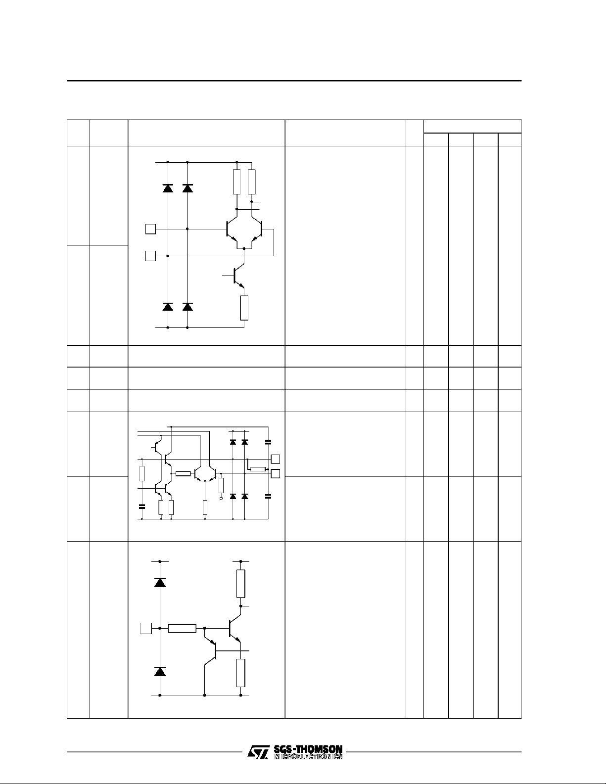
PIN DESCRIPTION
Pin
Symbol Equivalent circuit Description I/O
N
Standard
Min. Typ. Max. Unit
1 LST
36 PCK
GND
2kΩ
V
EE
GND
600Ω 600Ω
4kΩ
2kΩ
36
V
CC
PLL lock detection. Is High
while PLL locked. If
unlocked,becomes irregular.
At free running (TN1 H)
1
turnsLow
H
L
1601A-02.EPS
Clock output frequency
divided to 1/10 VCO output.
Used to check VCO free
running frequency
H
L
O
-1.0
-4.0VV
O
-0.8
-1.6
V
V
3SX
4SY
2/17
GND
240Ω
V
EE
V
CC
30Ω
100Ω 100Ω
30Ω
1601A-03.EPS
V
CC
Differential Serial Output
Inputparallel data is
34
converted to serial, then
O
from scrambled NRZ to
NRZI data
V
R3
2kΩ 2kΩ115Ω
V
EE
1601A-04.EPS
H
L
-1.6
-2.4
V
V
1601A-01.TBL
Page 3

PIN DESCRIPTION(continued)
Pin
Symbol Equivalent circuit Description I/O
N
Parallel data and clock input
buffers power supply. When
this pin is connectedto +5V,
29 V
6
7
8
9
10
11
12
13
14
15
16
17
18
19
20
21
22
23
24
25
CC
D9X
D9Y
D8X
D8Y
D7X
D7Y
D6X
D6Y
D5X
D5Y
D4X
D4Y
D3X
D3Y
D2X
D2Y
D1X
D1Y
D0X
D0Y
29
6
7
V
R3
2kΩ
V
EE
parallel data clockturns to
TTL mode. When this pin is
connected to GND, parallel
data clock turns to ECL
1kΩ
mode.
Parallel input ports:
LSB : D0X or Y
MSB: D9Xor Y
Signal :DnX
Return : DnY
For ECL mode, V
0V
H
L
ForTTL mode, VCC shall be
+5V
H
L
1601A-05.EPS
CC
shalll be
STV1601A
Standard
Min. Typ. Max. Unit
-
-1.0
-1.6
2.0
0.8
V
V
V
V
28 RSE
2kΩ
10kΩ 10kΩ
70kΩ
GND
28
V
EE
VCO range selection
H : highrange 140 to 270MHz
L : low range 100 to 145MHz
H
L
1601A-06.EPS
I
-0.4
-4.0VV
1601A-02.TBL
3/17
Page 4
STV1601A
PIN DESCRIPTION(continued)
Pin
Symbol Equivalent circuit Description I/O
N
V
CC
2kΩ 2kΩ
30 PCX
Standard
Min. Typ. Max. Unit
30
31
V
R3
31 PCY
V
EE
2, 5,
GND GND
32
26 V
27 V
EE
EE
GND
V
CC
33 FV
1kΩ
1kΩ
V
Ω
1k
1kΩ10k
9
Ω
34 TRP
1kΩ
2µF
V
EE
2kΩ
0.022µF
220Ω
0.1µF
Parallel clock (PCX) and its
return (PCY)
For ECL mode, V
H
CC
L
For TTLmode, V
CC
H
L
1601A-07.EPS
-5V power supply
I/O bufferPLL
-5V power supply
Logic part
VCO free runningfrequency
adjustment :
level gives the lowest
V
EE
frequency. Toadjust, set
34
TN1 high.
33
VCO input and phase
comparator outputshould be
connected to a parallel clock
frequency trapfilter to
minimize jitter
1601A-08.EPS
=0
= +5V
I
-1.0
2.0
-5.2 -5.0 -4.8 V
-5.2 -5.0 -4.8 V
I
-3.9 V
O
-3.2 V
-1.6
0.8
V
V
V
V
35 TN1
4/17
V
CC
GND
12kΩ
Test mode :
20kΩ
1
V
4k
Ω
V
High : VCO free running
condition (input disabled)
Low :Normal mode (input
enabled)
R3
EE
1601A-09.EPS
I
-1.0
-4.5VV
1601A-03.TBL
Page 5
BLOCK DIAGRAM
STV1601A
PCY PCX TN1 FV TRP RSE PCK
353031 33 34 28 36
37 N.C.
LST
SX
SY
1
3
4
PLLLOCK
DETECTOR
NRZ ⊗
NRZI
PARALELL TO SERIAL CONVERTER
6 7 8 9 10 11 12 13 14 15 16 17 18 19 20 21 22 23 24 2529
V
CC
D9X
D9Y
D8X
PHASE
DETECTOR
Parallel Clock
94
X +X + 1 SCRAMBLER
10-BITX3 WORD SHIFTREGISTER
D8Y
D7X
D7Y
D6X
D6Y
D5X
D5Y
VCO
D4X
D4Y
D3X
D3Y
Serial Clock
D2X
TIMING
GENERATOR
D2Y
D1X
Parallel Load
000hex
DETECTOR
D1Y
D0X
32
26
27
D0Y
ABSOLUTE MAXIMUM RATINGS
Symbol Parameter Value Unit
I
T
V
V
V
OUT
oper
T
P
EE
CC
IN
stg
D
Supply Voltage -6 V
Supply Voltage +6 V
Input Voltage VEEto V
CC
Output Current -30 mA
Operating Temperature 0 to 65
Storage Temperature -50 to 125
Allowable Power Dissipation 2.0 W
2
GND
5
GND
GND
V
EE
V
EE
1601A-10.EPS
V
o
C
o
C
1601A-04.TBL
RECOMMENDED OPERATINGCONDITIONS
Symbol Parameter Value Unit
V
EE
V
CC
T
oper
* For TTL input. Voltages are given with respect toGND
Supply Voltage -4.8 to -5.2 V
Supply Voltage * 4.8 to 5.2 V
Operating Temperature 0 to 65
o
C
ELECTRICALCHARACTERISTICS (VEE=-5V, VCC= GND/+5V, TA=25oC unless otherwise speciied)
Symbol Parameter Test Conditions Test Circuit Min. Typ. Max. Unit
DC CHARACTERISTICS
I
I
Supply Current 1
EE
Supply Current 2 7 mA
CC
Figure 2
140 mA
5/17
1601A-05.TBL
1601A-06.TBL
Page 6
STV1601A
ELECTRICALCHARACTERISTICS (VEE=-5V, VCC= GND/+5V, TA=25oC unless otherwise speciied)
Symbol Parameter Test Conditions Test Circuit Min. Typ. Max. Unit
DC CHARACTERISTICS
V
IH
V
IL
V
V
V
V
V
V
V
V
V
V
V
V
Input Voltage
IH
IL
I
IH
Input Current PCX, PCY, DnX, DnY Figure3
I
IL
IH
IL
Input Voltage
IH
IL
OH
OL
OH
Output Voltage
OL
OH
OL
AC CHARACTERISTICS
f
MAX1
f
MIN1
f
MAX2
f
MIN2
f
f
f
f
f
f
f
OP1
f
OP2
VCO Max. Oscillation Frequency 1
VCO Min. Oscillation Frequency 1 14.0 MHz
VCO Max. Oscillation Frequency 2
VCO Min. Oscillation Frequency 2 10.0 MHz
HP1
LP1
HP2
PLL Pull in Range
LP2
HP3
LP3
PLL Generator Frequency
tjit Jitter
Tested through PCK : 1/10 of serial clock.
= GND
V
CC
PCX, PCY, DnX, DnY
VCC= +5V
PCX, PCY, DnX, DnY
RSE Figure 7
TN1 Figure 6
PCK
=1kΩ
R
P
LST
= -10µA, IOL= +10µA
I
OH
Figure 5
SX, SY
= 220Ω
R
P
RSE = ”H”
Figure 4 30.0 MHz
RSE = ”L”
f signal = 270MHz
Figure 1 27.7 MHz
RSE = ”H”
f signal = 177MHz
RSE = ”H”
f signal = 143MHz
RSE = ”H”
RSE = ”H” 14.0 27.0 MHz
RSE = ”L” 10.0 14.5 MHz
f signal = 270MHz
RSE = ”H”
Figure 8 ±0.25 nsec
-1.0 V
-1.6 V
2.0 V
0.8 V
5 µA
-1 +1 µA
-0.4 V
-4.0 V
-1 V
-4.5 V
-0.8 V
-1.6 V
-1.0 V
-4.0 V
-1.6 V
-2.4 V
15.0 MHz
25.5 MHz
18.8 MHz
16.5 MHz
15.0 MHz
13.0 MHz
1601A-07.TBL
SWITCHINGCHARACTERISTICS (VEE= -5V, VCC=GND/+5V, TA=25oC unless otherwise speciied)
Symbol Parameter Test Conditions Test Circuit Min. Typ. Max. Unit
t
Rise Time
r
Fall Time 1.4 nsec
t
f
t
Rise Time
r
t
Fall Time 0.7 nsec
f
PCK
=1kΩ
R
P
SX, SY
= 220Ω
R
P
Figure 10
0.8 nsec
0.7 nsec
TIMING RELATIONOF INPUTCLOCK AND DATA
Symbol Parameter Test Conditions Test Circuit Min. Typ. Max. Unit
t
6/17
Pulse Width PCX, PCY
w
t
Delay Time PCX - Dn -5 +5 nsec
d
Figure11
-5 + tc/2 tc/2 +5 + tc/2 nsec
1601A-08.TBL
1601A-09.TBL
Page 7

Figure1 : TestCircuitDiagram Example
HP8182A
SIGNAL
ANALYZER
STV1601A
LED
-5V
0.1
22kΩ
9
6
10
D8
D9
TN1
AIY
AIX
26
-5V
-5V
DIX
33
25
41pF
73Ω
0.1
0.1
330Ω
ON : AF FREQUENCY ADJUST
SW3
10µF
5
0.1
10kΩ
-5V
-5V
R2
V
ADJUST
VCO FREQUENCY
QSW
DIY
34
DPR
FV
ESO ESIRSE
35
Ω
100k
36
37
1
22
0.1
220Ω
220Ω 220Ω
-5V
211918
EVR
SX4
SW2
A
Ω
10k
-5V
PCK
ADS32
17
D0
D1
10µF
B
0.1
1kΩ x8
-5V
CX
29
Ω
100
1
OUT
SERIAL
75Ω
0.1
STV1389AQ
0.1
Ω
220
16
D2
MON31
220Ω
15
14
D3
D4
STV1602A
QFS
28
SERIAL
2
75Ω
0.1
0.1
131211
D5D6D7
41pF
IN
Ω
150
Ω
150
Ω
220
Ω
220
FREQENCY
MONITOR
1kΩ x4
TRS DETECTOR
SIGNAL
10/16V
-5V
0.1 0.1
7
8
24 27 30 23
2
CABLE INPUT
A
INPUT SELECT
EE
GND V
20SYN
SY
3
DIGITAL INPUT
B
INPUT LEVEL
+5V
+1.4V
TTL
GND
-1.3V
ECL
SW2
ON : AF FREQUENCY ADJUST
-5V
-5V
Ω
22k
35
TN1
33 28
FV RSE
D0Y
25
SW1
VCO RANGE SELECT
A
B
HIGH RANGE
A
10kΩ
LOW RANGE
B
-5V
-5V
R1
V
ADJUST
VCO FREQUENCY
1601A-11.EPS
D6Y
13
4
SY
D.U.T.
STV1601A
D5Y
D5X
14
15
Ω
220
Ω
220
D4Y
D4X
161718
0.1
150pF 0.22µH
34TRP
D2Y
D2X
20
21
SIGNAL
GENERATOR
D1Y
D1X
222324
10µF/10V
D0X
-5V
D3Y
D3X
19
HP8180A
1kΩ
PLL LOCK
PCY
31
DETECTOR
1
36PCK
D9Y
D9X
6
7
3
SX
LST
D6X
D7Y
D7X
D8Y
D8X
8
9
101112
FREQUENCY MONITOR
0.1
10/16V
V -5V
10/16V
CC EE
V
0.1
R
V
0.1
37
N.C.
EE
V
CC
GND V
253229 27 26
PCX
30
7/17
Page 8

STV1601A
Figure2
Figure4
V +5V
CC
I
CC
AA
0.1
2 5 32 29
GND
V
CC EE
STV1601A
FV RSE TN1
10k
Ω
V
R1
-5V -5V
V -5V
EE
27 26
V
PCX
SX
SY
352833
10µF
22kΩ
I
EE
10/16V10/16V
0.1
1kΩ
30
220Ω
3
220Ω
4
-5V
0.1µF
POSITION
SW1 ON
SW1
1601A-12.EPS
V
-0.8V
-1.6V
1
V
2
-1.6V
-0.8V
11 12
V
1
A1 A2
I
IH
I
IL
V
2
I
IL
I
IH
2 5 32 29 27 26
GND
V
CC EE
3031PCX
STV1601A
PCY
FV RSE TN1
SW1
10kΩ
V
R1
-5V -5V
-5V
-5V
10/16V
0.1
V
1kΩ
30
PCX
220Ω
3
SX
220Ω
4
SY
352833
-5V
0.1µF
POSITION
SW1
10µF
SW2
ANY
ONSW2
AB
22k
Ω
1601A-13.EPS
8/17
Page 9

Figure4
STV1601A
-5V
10/16V
0.1
Figure5
V
-0.8V
-1.6V
2 5 32 29 27 26
GND
STV1601A
FV RSE TN1
SW1
10kΩ
V
R1
-5V -5V
V
V
2
1
V
-1.6V
-0.8V
OH
V
OL
V
CC EE
AB
-5V
352833
V
PCX
SX
SY
10µF
22k
FREQUENCY
MONITOR
1kΩ
30
220Ω
3
220Ω
4
-5V
0.1µF
POSITION
SW2
SW1
VCO RANGE
AONB
ONSW2
HIGH LOW
Ω
1601A-14.EPS
-5V
10/16V
0.1
2 5 32 29 27 26
GND
V
CC EE
V
3031PCX
STV1601A
PCY
1LST
V
V
V
1
2
FV RSE TN1
352833
POSITION
SW1
SW1 OFF
10µF
SW2
ANY
SW2
AB
10kΩ
V
R1
-5V -5V
-5V
22k
Ω
1601A-15.EPS
9/17
Page 10

STV1601A
Figure6
-0.8V -1.6V
Figure8
Figure7
-5V
10/16V
0.1
2 5 32 29 27 26
GND
V
V
V
1
3031PCX
PCY
TN131
CC EE
STV1601A
1LST
V
1
V
FV RSE
2 5 32 29 27 26
GND V
28 RSE
CC EE
STV1601A
FV TN1
2833
10kΩ
V
R1
-5V
1601A-16.EPS
10kΩ
V
R1
-5V -5V
3533
V
PCX
SX
SY
10µF
22k
-5V
Ω
10/16V
0.1
30
3
4
FREQUENCY
MONITOR
1kΩ
220Ω
220Ω
SW2
-5V
0.1µF
1601A-17.EPS
Parallel
clock
data
2 5 32 29 27 26
GND
V
CC EE
STV1601A
RSE
FV TN1
10kΩ
V
R1
-5V
3533
28
10µF
22kΩ
-5V
10/16V
V
PCX
SX
SY
-5V
0.1
FREQUENCY
MONITOR
1kΩ
30
3
4
220Ω 220Ω
-5V
SW2
0.1
0.1µF
-5V
220Ω
TRIGGER
STV1389AQ
-5V
0.1 75Ω
0.1
150Ω150Ω
0.1µF
SIGNAL 270Mb/s
75Ω
1
2
SERIAL OUT
SIGNAL
t
jitter = 1/2
1601A-18.EPS
10/17
Page 11

STV1601A
Figure9 : tr,tfDefinition
80%
20%
tt
rf
Figure10 : td,tWDefinition
t
c
t/2
c
t/2
c
50%
t
d
t
w
DESCRIPTION
STV1601A internally generates a 10 times clock
frequencylocked to the parallelinput clock thanks
toabuilt-inPLLand convertsinputparalleldatainto
Figure11 : PhaseRelation between Clock andData
serial data.
To easeclock extractionat thereceivingend,serial
datais scrambled.To minimize polarityeffect,serial
datais then convertedto NRZI andoutput in differential mode.
APLLlock detectioncircuit only enables the serial
output when locked.
1. Phase relation between input parallelclock
and data
1601A-19.EPS
Thephase relationbetween the parallel clock and
the dataisshown in Figure11.Both clockand data
are differentialinputs
Parallelclockanddataaresuchthattherisingedge
ofPCX should be atthe middleofthe data. Aclock
havingthe samephase as PCXis internallygeneratedin order to latch the data.
2. TTL input operation
Parallel clock and data can be either TTL or ECL
inputs. Touse as TTL inputsVCC (Pin 29) shallbe
connected to +5V. A fixed bias of +1.4V shall be
appliedto PCY and DnY (n = 0 to 9). TTL signals
and their parallel clock will be provided through
1601A-20.EPS
1kWresistors to each ”X”input. These1kW resistors are effective to minimize the influence of the
TTLinput signalsto the jittercharacteristics of the
serial outputsignal. For8-bit data, unused LSB(s)
must befixed Low. Fixedbias value can be higher,
for example,2.5V in case of CMOSinputs.
PCX (Input)
DATA (Input)
PCX (Output)
Figure12 : TTL Input Operation
+5V
STV1601A
V
CC
29 30 31 5 7 26 25
1kΩ 1kΩ 1kΩ
Parallel
Clock
Parallel
Data
TTLParallel Signal
D0YD0XD9YD9XPCYPCX
+ 1.4V for TTL
+ 2.5V for CMOS
1601A-21.EPS
1601A-22.EPS
11/17
Page 12

STV1601A
3. PLL block
PARALLELCLOCK INPUT CONTROL
PLL, PLL lock detection and the various blocks of
the serial output control are shown in Figure 13.
When TN1 is connected to GND (set High), the
parallel clock input is disabled.
The VCO turns to free running conditions and its
frequencycan be adjustedthrough FV.
This frequencydecreaseswhen the resistor value
between FV and V
is reduced. Oscillation fre-
EE
quency monotoring is performed through PCK
whichdelivers a frequencydivided byten.
When PLL is locked, PLL and PCX input signal
phases are nearly matched.The RC network connected to TN1, temporarily, disables the parallel
clockin orderto avoid mislocking problems.
VCO oscillationfrequency range selection isavailable through RSE ; High : from 140 to 270MHz ;
Low : from100 to 145MHz.
TRP (Pin 34) is the phase comparator output. To
minimize jitter, a trap circuit, consisting in a serial
tuned circuit at parallel clock frequency can be
used.
Figure13 : PLLand Serial Output ControlBlock
PLL LOCK DETECTION
The LSTsignalis generatedby latching theincom-
ing parallel clock by theinternal one (whichis 1/10
of theVCO frequency).LST is usedas a PLLlock
detection signal andalso controlsthe serialoutput.
If the parallel clockinput is disabled (by means of
TN1), LST turns Low and the serial output is disabled as described in the previous section (SX
(Pin 3) =High, SY (Pin4) = Low).
If the serial output has to be disabled while no
parallel clock input is provided, PCX must be set
Low and PCYmust beset High.
4. Sync word
Toconvert serial data back to parallel, insertion of
some timingreference data indicatingthe parallel
data word boundary in the serial data is needed.
This,called TRS (TimingReference Signal) in the
digital interface format, consists of the three consecutivewords 3FFH, 000H,000H.
Conversionto 10-bit TRS from 8-bit (TRS)
8-bit parallel data
8-bit paralleldatacan beconvertedinto 10-bitdata
by using the 8th bit as the MSB and by setting the
2 LSBs at logicalstates as shown in Figure 14.
LST
SX
SY
PCY PCX TN1 FVTRP RSE PCK
”0”
QDQD
PHASE
COMPARATOR
NRZToNRZI
CONVERSION
Serial Clock
VCO
SCRAMBLER
1/10 DIVIDER
1601A-23.EPS
12/17
Page 13

STV1601A
Figure14 : 8-bit Parallel Input Data (ECLlevel)
STV1601A
242322
9+x4
D0YD0X
25
+1.
621
8-bit Parallel Data
D1X D1Y
Ω
10k
V
EE
The conversion algorithm detects 2 successive
000H words and setsthe twoLSBs ofthe previous
word,which is supposedtobe FF, accordingto the
standard.
Figure10 : Conversionfrom 8-bit TRS to
10-bit TRS
Input Order
MSB
0
LSB
Parallel Data after ConversionInput Parallel Data
001
001
001
001
001
001
001
001
00
0011
Input Data
Fixed Data
001
001
001
001
001
001
001
001
00
000
Conversionin the caseof more than three successive ”000H” words.
If more than 3 consecutive words of 000 in D1
standard, or 4 consecutive words of 000 in D2
standardoccur atthe parallelinput (illegal according to the standard), thus no proper operation is
possible.
5. Scramblingand NRZ to NRZI conversion
Figures16 and17 show the scramblingcircuit,the
scrambling polynomialis as follows : x
Figure16 : (x9+x4+1) BasicScrambling Circuit
D1 D2 D3 D4 D5 D6 D7 D8 D9
Figure17 : (x9+x4+1)Basic Scrambling Circuit
D1 D2 D3 D4D5D6 D7 D8 D9
1601A-24.EPS
To eliminatesignal polarityofscrambleddata, conversionfrom NRZto NRZIis performed (Figures18
and 19).
Therefore, the polarity for output distribution or
receivingis not needed. This allows easy system
design.The NRZ toNRZI polynominalis x +1.
VCO temperature compensation and oscillation
frequencyadjustment
VCO oscillation frequency depends on the temperature as shown in Figures 22 and 23 ”Representative characteristics examples”. Within the
normal range of operation, frequency increases
with temperature.FV voltageremains almost constant regardless of temperature. Figure 20 shows
an exampleof atemperature compensationcircuit
using a diode (transistor with C-B diode short-circuited) and a resistorconnected between FV and
1601A-25.EPS
. Examplesof representativecharacteristicsfor
V
EE
varioustemperaturesare shown in Figures22 and
23concerningoscillationfrequencyandPLLpull-in
range (signalfrequency 270, 177and 143MHz).
VCO free running frequencyadjustment
VCO free running frequency adjustment is performedat room temperature.
If TN1 is set High, VCO free runs. Wait for 5 to
10 minutes after turning power supply ON (warm
up time). While monitoring PCK output (Pin 36)
adjust the signal frequency (within ± 1%) with the
variableresistor connected betweenFV and V
EE
1601A-26.EPS
1601A-27.EPS
.
13/17
Page 14

STV1601A
Figure19 : Relation between NRZ and NRZI Signals
Time scale
NRZ signal
NRZI signal
NRZ to NRZI conversion
NRZI signal
NRZI inverted signal
NRZ to NRZI conversion
Figure20 : VCO TemperatureCompensationand Free Running Adjustment
STV1601A
TN1
35 33 36
10µF 22kΩ
34
C1
Jitter trap
Sincethe internallygeneratedserialclockislocked
to the incomingparallel clock,there exists periodic
jitter components which are generated from the
phase comparisonprocess of the PLL.
Aserial resonantcircuit (trap)connected between
TRP (Pin 34) and V
tuned at the parallel clock
EE
frequency reduces effectively the fundamental
componentof the jitter well below the specification
(±0.25ns).
Recommendedvalues of C1 and L1 are given in
the followingtable.
L1
FV
Smallsignal
transistor
10k
PCKTRP
Frequency monitor
1kΩ
Ω
V
EE
RECOMMENDED VALUESOF THE TRAP CIRCUIT
COMPONENT
C1 (pF) 150 240 300
L1 (µH) 0.2 0.3 0.4
An important remark in a practicalimplementation
is that TRP node is an input of a very sensitive
voltage-frequency converter (VCO) which can be
easily disturbedby any pick-upnoise.
Hence, the trap circuit should be carefullylocated
and bekeptas short as possiblefrom the Pin 34 in
order to avoid noise problems.
D1
1601A-29.EPS
1601A-30.EPS
STANDARD
D2
PAL NTSC
14/17
Page 15

Figure21 : Application CircuitExample
68Ω
For signal
Processig
220Ω
220Ω
1kΩ
0.1µF
STV1601A
processing
68Ω
0.1µF
For coaxialcable
Test
Jumper
10µF/16V
-5V
150Ω
Recommendedvalues
34
TRP
nF
µH
Unit
0.4
300
NTSC
D2
0.3
PAL
D1
0.2
151 210
L1
C1
-5V
Q1
L1
C1
10kΩ
33
32
FV
GND
(Return)
0.1
31
PCY
Parallel
Clock In
30
PCX
0.1
51Ω
LOW
EE
V
EE
V
D0Y
D0X
-5V((115mA typical)
26 27
25
24
Ω
51
Ω
2.2k
Ω
4.7k
-5V
D2 NTSC
D1,D2 PAL
10kΩ
HIGH
29
28
CC
V
RSE
(Rateselect)
-5V
150Ω
0.1µF
0.1µF
STV1389AQ
22kΩ
1kΩ
35
TN1
LST
SX GND
SY
Ω 220Ω
220
ParallelClock
37
N.C.
0.1µF
-5V
-5V
Test Ponit
36
PCK
220Ω
123
4
5678
STV1601A
(ENCODERMODULE)
D9Y D9X GND
D8X
9
D8Y
D7X
10
D7Y
11
D6X
12
D6Y
13
D5X
14
D5Y
D4X
15
(ECL Balanced Pair)
Parallel Data IN
D4Y
17
16
D3X
18
D1YD1XD2Y
D2X
D3Y
23
22
21
2019
1601A-31.EPS
15/17
Page 16

STV1601A
EXAMPLEOF REPRESENTATIVECHARACTERISTICS
Figure22 : VCO Oscillation Frequencyversus
FV PinVoltage
RSE: ”H”
300
65°C
260
220
180
140
VCO oscillationfrequency(MHz)
0.80 0.90 1.00 1.10 1.20 1.30
85°C
FV pin Voltage (V)
25°C5°C
45°C
-15°C
Figure24 : Pull in Rangeand Free Run Fre-
quency (270Mb/s)
30
29
28
27
26
25
Frequency(MHz)
24
23
-155 25456585
Highpull in
Free run
Low pull in
Ambienttemperature(°C)
Figure26 : Pull in Rangeand Free Run Fre-
quency (143Mb/s)
18
17
16
15
Freerun
14
13
Frequency(MHz)
12
11
-155 25456585
Ambienttemperature(°C)
Highpull in
Low pull in
Figure23 : VCO OscillationFrequency versus
FV Pin Voltage
25°C
45°C
5°C
-15°C
1601A-32.EPS
150
140
130
120
110
100
VCO oscillationfrequency(MHz)
0.90 1.00 1.10 1.20 1.30
65°C
85°C
FV pin Voltage (V)
Figure25 : Pull in Rangeand Free Run Fre-
quency(177Mb/s)
21
Highpullin
Low pull in
1601A-34.EPS
1601A-36.EPS
20
19
18
Freerun
17
16
Frequency (MHz)
15
14
-15 5 25 45 65 85
Ambienttemperature(°C)
RSE : ”L”
1601A-33.EPS
1601A-35.EPS
16/17
Page 17

PACKAGE MECHANICALDATA
37 PINS - CERAMICPGA
Dimensions in mm
3.8
1.15 0.15
4.2
STV1601A
25.4 0.5
0.2
Seating plane
0.46 0.051.2 0.1
2.54x 9=22.86 0.25
Bottom
View
2.54 x 9 = 22.86 0.25
Pin 10 Pin 1
2.032 max.
Pin 37
2.54
Pin 28Pin 19
Pin 36
2.54
25.4 0.5
PM-PGA37.EPS
Information furnished is believed tobe accurate and reliable. However, SGS-THOMSON Microelectronics assumes no responsibility
for the consequences of use of suchinformation nor forany infringementof patents or other rights of third parties which may result
from its use. No licence is granted by implication or otherwise under anypatent or patent rights ofSGS-THOMSON Microelectronics.
Specifications mentioned in this publication are subject to change without notice. This publication supersedes and replaces all
information previously supplied.SGS-THOMSON Microelectronics products are not authorized for use as critical components in life
support devices or systems without express written approval of SGS-THOMSON Microelectronics.
1994 SGS-THOMSON Microelectronics - All Rights Reserved
Purchase of I
2
I
C Patent.Rights to use these components in a I2C system, is granted provided that the system conforms to
2
C Components of SGS-THOMSON Microelectronics, conveys a license under the Philips
2
the I
C Standard Specifications as defined by Philips.
SGS-THOMSON Microelectronics GROUP OF COMPANIES
Australia - Brazil - China - France - Germany - Hong Kong - Italy -Japan - Korea - Malaysia - Malta - Morocco
The Netherlands - Singapore - Spain - Sweden - Switzerland - Taiwan - Thailand - United Kingdom - U.S.A.
17/17
 Loading...