

Page 1

March 2003 ADCS 7283313C 1/44
STV0681
DUAL-MODE DIGITAL CAMERA CO-PROCESSOR
®
DESCRIPTION
STMicroelectronics Imaging Division has produced
the camera co-processor STV0681 which, used
with CIF/VGA sensors as part of a low cost dualmode camera chipset, allo ws a new line of low cost
cameras or toy products to be brought to the
market. STV0681 is a mask ROM version of
STV0680B, programmed with v3.00 Firmware.
FEATURES
ST have maintained the standard features already
available in the successful STV068B chipset,
including:
● Support for VV6411 (CIF) and VV6501 (VGA)
CMOS imaging sensors.
● Support for SDRAM sizes 16MBit (up to 20
CIF images) or 64Mbit (up to 80 CIF or 26
VGA images).
● Low resolution “economy” mode allows for
more images to be stored.
● High frame rate web cam (tethered video)
over USB.
● Audio record/playback and “Delete Last”
function
● Custom sounds playback (e.g. “Talking” or
“Musical” camera)
● Support for an OEM Flashgun module
● Automatic anti-flicker exposure control.
● Image up load over RS232 or USB.
● Driver support for Win98/Win2k/WinME and
MacOS 8.6/9.0/9.1.
● Continuous capture while untethered (except
when Flashgun enabled) and downl oading to
AVI file format
● Power-saving “stand-by” mode which
maintains memory contents.
● Simple user interface including 2 buttons,
status LCD display, and buzzer.
● Evaluation Kit (EVK) available.
● Software De velo pment Kit (S DK) allo ws OEM
PC Software applications to be written.
● Quick Power Down (by holding M ode Butto n).
● “Delete Last” Function
Audio Record and Playback
The enhanced features included in STV0681 allow
audio memos to be recorded at a sampling rate of
11kHz, by adding a microphone and comparator
chip, and by utilizing the pre-amplifier included in
CIF/VGA sensors such as VV6411 and VV6501
respectively.
These sounds can be uploaded to the PC ov er USB
or RS232, and played back using a Software
application developed by the OEM using the SDK.
Demonstration PC software with source code is
available with the Evaluation Kit (EVK). With
suitable OEM software, the camera could even be
used to record comments about pictures or video
clips in a “dictaphone” fashion, with the audio
commentary played back when viewing the
pictures/video.
Recorded audio sounds can also be pla yed b ack on
the camera, with the addition of an amplifier chip
and speaker or headphone socket.
By auto-detecting hardware, STV0681 will only
enable these additional functions if audio har dw are
is fitted. Actual hardware implementation is the
subject of a separate STV0681 Reference design
(see
Chapter 10
).
Evaluation Kit and Reference Design
Evaluation kits are available for STV0681 features.
Precise design guidelines are a vailable from ST as
a reference design manual (see
Chapter 10
).
Note: Simultaneous audio record and
continuous video capture is not possible.
Page 2

STV0681
2/44 ADCS 7283313C
Table of Contents
Chapter 1 Introduction . . . . . . . . . . . . . . . . . . . . . . . . . . . . . . . . . . . . . . . . . . . . . . . . . . . . . .5
1.1 Digital camera chipset ..........................................................................................................5
1.2 Key system features .............................................................................................................6
Chapter 2 Detailed Features . . . . . . . . . . . . . . . . . . . . . . . . . . . . . . . . . . . . . . . . . . . . . . . . . .9
2.1 Sensor type and image formats ...........................................................................................9
2.2 User interface .....................................................................................................................10
2.3 Battery level detect and USB auto-switch ..........................................................................12
2.4 Audio record and playback .................................................................................................12
2.5 PC interface options and software support ........................................................................13
2.6 Anti-flicker exposure and gain control ................................................................................14
Chapter 3 Camera Modes of Operation . . . . . . . . . . . . . . . . . . . . . . . . . . . . . . . . . . . . . . . .15
3.1 Modes available .................................................................................................................15
3.2 Description of modes .........................................................................................................16
Chapter 4 STV0681 Hardware Interfaces . . . . . . . . . . . . . . . . . . . . . . . . . . . . . . . . . . . . . . .18
4.1 Sensor interface .................................................................................................................18
4.2 Memory interface ...............................................................................................................18
4.3 USB interface ...................................................................................... ........... ........... .........21
4.4 UART module for RS232 interface .....................................................................................22
4.5 Power management and battery type ................................................................................23
4.6 Quartz crystal .....................................................................................................................24
4.7 Numeric LCD interface .......................................................................................................24
4.8 Switches and LED’s ...........................................................................................................25
4.9 Flashgun hardware interface ..............................................................................................26
4.10 IR filter .......................................... ......................................................................................26
Chapter 5 Customising the STV0681 . . . . . . . . . . . . . . . . . . . . . . . . . . . . . . . . . . . . . . . . . .27
5.1 External EEPROM .............................................................................................................27
5.2 EEPROM data format ........................................................................................................28
5.3 Programming the EEPROM ............................................................................................... 28
Page 3

ADCS 7283313C 3/44
STV0681
Chapter 6 Software support . . . . . . . . . . . . . . . . . . . . . . . . . . . . . . . . . . . . . . . . . . . . . . . . .29
6.1 General features ................................................................................................................29
6.2 Software installation ...........................................................................................................30
Chapter 7 Detailed Chipset Specifications . . . . . . . . . . . . . . . . . . . . . . . . . . . . . . . . . . . . .31
7.1 Typical camera specifications ............................................................................................31
7.2 Absolute maximum ratings .................................................................................................31
7.3 STV0681 specifications ......................................................................................................32
7.4 USB specifications ............ ........... ........... ...........................................................................32
7.5 DC characteristics ..............................................................................................................33
7.6 PLL characteristics .............................................................................................................33
7.7 Crystal tolerance ............... ........... ........... ........... ................................................................33
7.8 Typical current consumption of complete camera ..............................................................34
Chapter 8 STV0681 pin description . . . . . . . . . . . . . . . . . . . . . . . . . . . . . . . . . . . . . . . . . . .35
8.1 STV0681 pinout .................................................................................................................35
8.2 STV0681 pin description ....................................................................................................36
Chapter 9 STV0681 package mechanical data . . . . . . . . . . . . . . . . . . . . . . . . . . . . . . . . . .41
Chapter 10 Evaluation Kit (EVK) . . . . . . . . . . . . . . . . . . . . . . . . . . . . . . . . . . . . . . . . . . . . . . .42
10.1 Ordering details ..................................................................................................................42
10.2 Technical support ...............................................................................................................43
Page 4
STV0681
4/44 ADCS 7283313C
Document Revision History
Revision Draft Date Comments
A 1.0 May 2001 Initial release (product preview)
B 4.0 April 2002 Document status updated to datasheet.
Major changes: removed references of VV6410 and VV6444
sensors
C4.1November
2002
Removed all salestypes for imaging sensors:
removed section 6.1
addition of ch apter 5 - Customizing the STV0681
Replacement of section 6.1 - General features (i n Chapter 6 -
Software support)
Page 5

ADCS 7283313C 5/44
STV0681 Introduction
1 Introduction
1.1 Digital camera chipset
1.1.1 General
This document describes the features and functionality of a CMOS chipset, comprising an
STMicroelectronics (ST) CIF or VGA resolution sensor and an STV0681 companion processor, as
well as outlining what peripheral compone nts are required/supported in order to complete a camera
using the chipset. Such a camera is particularly suited to dual-mode digital st ills or t o y app lications .
1.1.2 Stills capture and image upload
In stills mode, the camera stores raw image data in memory. The camera features no colour
processing, ensuring its simplicity and low cost. Subsequent upload of raw data to a PC or
Macintosh for processing is done through an RS232 or USB interface, through demo software, a
TWAIN driver, or OEM custom application. The license to use the colour algorithm (embedded in
the PC or Mac driver software) is included in the price of the chipset.
1.1.3 Webcam Video over USB
A video option is provided, w hen tether ed throug h USB . It a llows f or Vi deo for Microsoft Window s
applications, and ‘video clips’ to be recorded while untethered by continuously capturing images in
‘continuous’ mode . Images are then do wnloaded to th e PC for playbac k, using softw are to create an
AVI file.
1.1.4 Audio features
The STV0681 allows audio memos to be recorded at a sampling rate of 11kHz. These sounds can
be uploaded to the PC over USB or RS232 and played on the PC, or they can be replayed on the
camera.
With audio playbac k hardw are fitted to the camera , it is possib le to do wnload a set of up to 20.WAV
file “sound bites”, to store in SDRAM, each of which can be linked to a particular camera function.
This allows f or camera “Theme Music”, custom sounds such as an imitation shutter “Clic k-Whirr”, o r
for certain functions to “talk” to the user, e.g. “Nice picture!”.
This has limitless possibilities for OEM language customizing or licensed character cameras.
Downloading sounds is possi b le wi th the use of an OEM appl ication de v el oped using the SD K, and
a demonstration PC application with source code is available with the EVK. Sounds are stored in
SDRAM and will therefore reduce the number of images/amount of audio which can be stored,
STV0681 calculates the remaining memory and displays the number of images left. Sounds can
only be stored when untethered while battery power is maintained.
1.1.5 Flashgun support
The addition of an OEM flashgun module increases the camera capabilities and improves low light
image quality. STV0681 flashgun support includes modified exposure control, an e nable input and a
correctly timed trigger output. Although it rem ains the responsibility of the OEM to source a suitab le
Flashgun module, advice on hardware interfacing, flash charge sensing and required flashgun
energy are given in a separate Flashgun Application Note (AN1312), please contact ST for details.
Page 6
Introduction STV0681
6/44 ADCS 7283313C
1.1.6 “Delete Last” function
An additional user interface function is available in STV0681 with either audio record or playback
hardware fitted. With these, the user can delete the last image or contin uous clip to be captured, or
the last audio memo to be recorded. The standard “C lear all” (“CL”) function remai ns, whether or not
audio hardware is fitted.
1.1.7 Backward compatibility with STV0680B
STV0681 is electrically and functionally compati ble with cameras desi gned for STV0680B , and uses
the same PC/Mac drivers, however the change of device pinout means that some PCB re-design
will be required.
Precise design guidelines are av ailab le from ST as a refer ence design (see
Chapter 10
). A software
develop ment kit (SDK) for PC is available from ST to interface to the camera and provide the basis
to develop a custom software application for stills and/or video. It includes colour processing
software.
1.2 Key system features
The key features of a typical camera based on the STV0681 chipset are listed here below.
1.2.1 Image features
● Support for CIF resolution sensor - 352 x 288 pixels
● Support for VGA resolution sensor - 640 x 480 pixels
● 80 picture storage capacity possible for CIF, with 64MB memory
● 26 picture storage capacity for VGA, with 64MBit memory
● A greater number of images can be stored when ‘Low’ resolution mode is enabled (e.g. 80 QCIF
images with 16Mbit memory, 107 QVGA images with 64Mbit memory). See
Table 1
.
● Automatic anti-flicker exposure and gain control
● Support for flashgun.
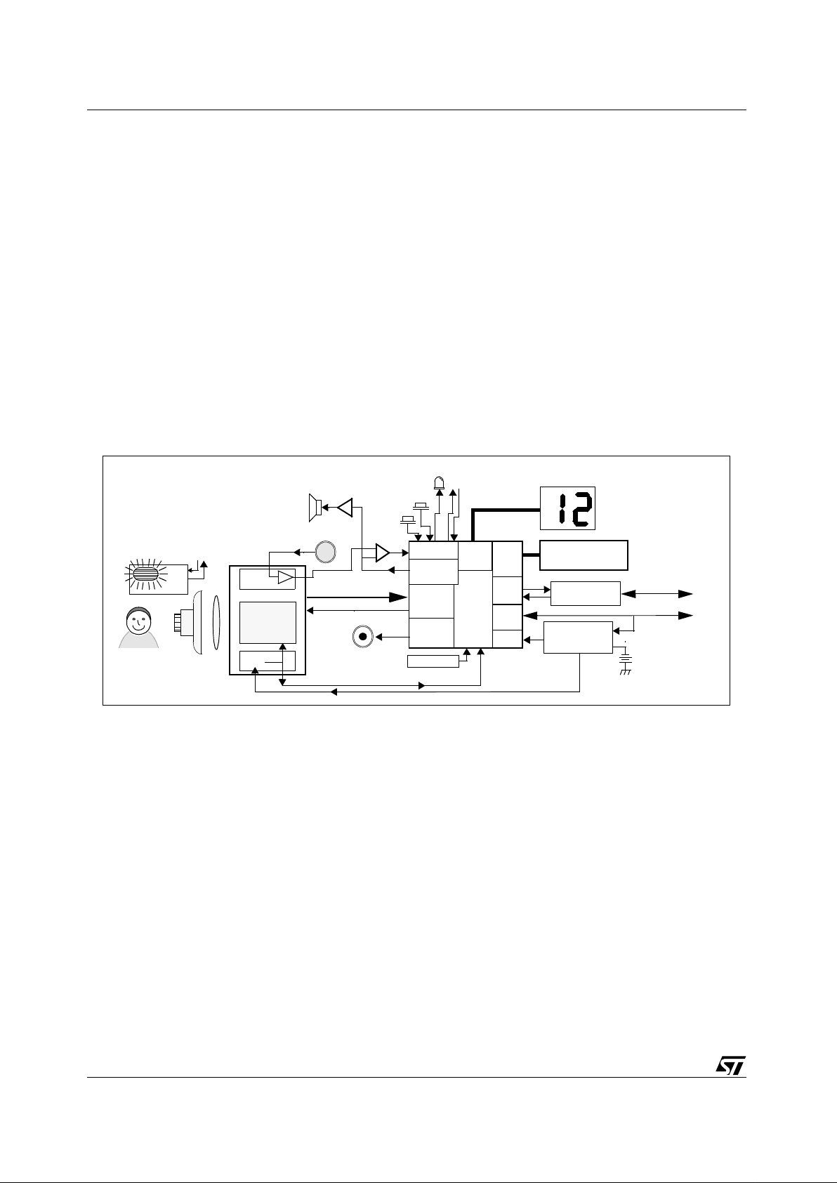
Figure 1: Typical camera system block diagram
CMOS Sensor
Sensor data
STV0681
USB interface
16MBit or 64MBit
SDRAM
Lens +
RS232
I/F
USB
I/F
memory
I/F
RS232 interface
GPIO
Sensor
I/F
PWM
LED
4.5 - 6v Battery e.g.
12MHz XTAL
Audio DAC
LCD
Driver
2x7seg.LCD
Push
Transceiver
Piezo
“Mode”
Buzzer
“Shutter
4-5v (Nominal) supplyfrom Battery or USB
3-4 x AA, AAA, etc.
Power
Management
Circuit (Discretes)
Detect Low
Battery
to PC
to PC
Circuit (Discretes)
Sensor clock
IR Filter
VV6501 (VGA)
VV6411 (CIF)
Image Array
Audio
Pre-Amp
Speaker
Microphone
Compara t or
Buttons:
/Record”
OEM Flashgun
Enable/Trigger
Module
Audio
Enable/Trigger
Flashgun
Amplifier
VReg
3v3 supply
Subject
Page 7

ADCS 7283313C 7/44
STV0681 Introduction
1.2.2 User features on camera
● Self-timer mode allows a picture to be captured after several seconds.
● Twin 7 segment LCD panel supported - showing number of pictures left, and modes.
● Picture counter helps the user to know how much memory is left.
● Un-tethered ‘Continuous’ mode allows capture of image sequences for storage in memory and
subsequent download to PC.
● Piezo buzzer indicates a number of useful events to the user, e.g. whether enough light is present for
picture capture, etc.
● LED indicator .
● “Clear all” function clears camera.
● “Low Resolution” mode increases number of images which can be captured by reducing image
resolution.
● Audio Record function (if audio record hardware detected) allows sounds to be recorded.
● Audio Playback function (if audio playback hardware fitted) allows sounds which have been recorded
to be played back.
● “Delete last” function allows user to delete audio memos, pictures or continuous clips, deletion must
be carried out “most reset first”.
● Camera can be configured by the user to play custom sounds at certain functions, using a PC
application.
● “Go to sleep” function, whereby the camera can be put into standby mode while untethered.
1.2.3 User features on PC software
PC software allows a number of features such as fast download of thumbnail images for picture
selection, and automatic detection and correction of sensor defects. The driver compatibility
includes:
● TWAIN driver to suit all TWAIN compatible imaging applications
● Video for Microsoft Windows PC driver for tethered video mode (through USB), available at all
resolutions, with fastest framerates at QCIF resolution
● AVI video file creation from image sequences captured in ‘continuous’ mode
● Quicktime Video driver and Adobe Photoshop stills plug-in for Mac
Custom OEM PC software can be de v el oped b y using the SDK (for SDK av ailabi lity, contact ST), to
upload thumbnails/still images or ‘continuous’ images, e.g. for AVI file creation.
The SDK (version 2.90 or later) allows:
● the OEM to write a custom application and upload sound memos based on the example LCDC demo
software.
● the OEM to write a custom application and download custom sounds to the camera based on the
example CustomSound software.
1.2.4 Power management features and USB compliance
● Retention of pictures, recorded sounds and downloaded custom sounds with extremely low power
operation. The camera seems to be “switched off”.
● Auto power-off after 30 seconds of non usage.
● Operates from 4.5-6V battery, although system voltage is 5V or 3.3V, dependant on sensor.
● Low battery detection.
Page 8

Introduction STV0681
8/44 ADCS 7283313C
● Dependant on hardware configuration, switch-over to USB power supply is supported and the device
can operate with low batteries or without batteries when connected to USB.
● Full USB compliance requirements are listed in the USB specificati on. How e ver, in a camera designe d
using this chipset, the following must at least be included: (a) an SDRAM with sufficiently low selfrefresh current, (b) USB inrush protection circuitry to maintain sufficient supply voltage to the 5V
sensor. See
Section 7
for further details.
1.2.5 General features
● High speed picture/sounds upload to PC/Mac over USB
● ST colour processing algorithms included under license (as part of drivers/SDK)
● USB or RS232 serial interface options, and VfW / TWAIN driver support.
Page 9
ADCS 7283313C 9/44
STV0681 Detailed Features
2 Detailed Features
2.1 Sensor type and image formats
The sensor type is auto-detected by STV0681, the correct sensor timing is enab led and the corr ect
image resolutions are enabled, as shown in
Table 1
.
For stills photogr aph y, ‘High’ or ‘Low’ resolution mode can be selected, to give CIF or QCIF pictures
from a CIF sensor , a nd V GA o r QVGA from a V GA sensor ( see
Table 1
). Reduced resolution allo ws
for storage of more images. Images captured in both ‘High’ and ‘Low’ resolution can be stored in
camera memory at the same time. Therefore there is no need to clear images stored in memory
prior to changing image resolution.
Where USB is connected, the host PC software (through a Video for Microsoft Windows driver)
can activate tethered video mod e, re gardle ss of the user inputs to the camer a b uttons . In this case ,
the image resolution is controlled by the PC driver.
Note: When tethered VfW video (PC) or Quicktime driver (Mac) is activated, all images or recorded
sounds or video clips are deleted from the camera SDRAM. A software solution is available
(“Camera control”, as p art of the SDK for PC , and “P lug’n Sav e” f or Mac) wh ich can monitor wheth er
a camera is connected and warns the user if activating the VfW driver causes SDRAM contents to
be deleted.
Note: 1 VfW framerate is dependent on PC performance and USB bus loading
2 The number of images which can be stored is reduced if Audio sounds have been recorded on the
camera or if custom sounds have been downloaded from the PC to the camera. The reduction of
capacity depends on the length of audio clip , b ut a rough guide is that if 1 CIF i mage uses the same
amount of SDRAM as 10sec of audi o , and one VGA image uses the sam e amount of S DRAM as 30
sec. of audio.
3 A CIF camera with ST V0681 an d 64Mbit SDRAM can store up to 320 images by using QC IF mode .
When more than 99 images are available, the LCD display remains at 99. When the number of
available images is inferior to 99, the LCD display shows the number of available images like in all
other modes.
Table 1: Image modes supported
Sensor
Image Size
Resolution
mode
Final Image Size
Max. no. of
images
stored in
16MBit
memory
(
Note 2
)
Max. no. of
images
stored in
64MBit
memory
(
Note 2
)
Approximate
VfW framerate
(
Note 1
)
CIF 352 x 288 High CIF 352 x 288 20 80 15 frames/sec.
Low QCIF 176 x 144
(Subsampled)
80 322
(see
Note 3
)
22.5 frames/sec.
VGA 640 x 480 High VGA 640 x 480 ( 6) 26 2 frames/sec.
Low QVGA 320 x 240
(Subsampled)
(26) 107
(see
Note 3
)
12 frames/sec.
Page 10

Detailed Features STV0681
10/44 ADCS 7283313C
2.1.1 IR filter
For IR filter design, the best choice filter follows the GS0034 dielectric stack filter specification
available from STMicroelectronics. An alternative, although not optimal filter, would be Schott
S8612 doped glass also sold as CM500.
2.2 User interface
The user interface supported by S TV0681 comprises of user controls , b uzzer sounds or customized
sounds and visual displays.
2.2.1 Push buttons
The following are the functions which are supported by the chipset. These functi ons are achie vable
with no more than 2 push buttons.
1 Mode button (wake-up/switch between modes)
This button allows the user (1.1) to wake the camera up from standby mode when the camera
is to be used for taking pictures, or (1.2) to switch between modes of operation shown in
Chapter 3
.
2 Shutter button (shutter/confirm action)
This button allows the user to take a picture or confirm an action, as shown in
Chapter 3
The modes of operation are described in
Chapter 3
.
It may also be desirable to include an on-off slider switch. The advantages and disadvantages as
well as its exact function are discussed in the reference design available from STMicroelectronics.
When a flashgun module is included in the camera, it is necessary to include a flash on/flash off
push button or slider switch depending on the exact flashgun module design. Possible
implementations are discussed in a separate application note AN1312 available from
STMicroelectronics.
2.2.2 LED indicator
The LED indicator displays the camera status when not in Standby/PC suspend mode.
2.2.3 Picture counter using 2 x 7 segment display
STV0681 stores a picture counter value indicating how many images can still be captured.
STV0681 supports a 2x7 segment LCD panel. In ‘Snapshot’ mode and continuous capture mode,
this LCD panel displa ys the number of pictures still a v ailab le. This is useful to identify w hen the user
is approaching the maximum number of images which can be stored (see
Table 1
). The user can
clear the images stored in memory and continue taking pictures. In other modes, this LCD panel
displays a 2-character code that helps the user to navigate around the modes.
Note: A CIF camera with STV068 1 and 64 Mbit SDRAM can stor e up to 320 im ages b y usin g QCIF mode .
When more than 99 images are still available, the LCD display remains at 99. When the number of
available images is inferior to 99, the LCD display shows how many images are available like in all
other modes.
For suitable numeric LCD panel types, see
Section 4.7
.
Page 11
ADCS 7283313C 11/44
STV0681 Detailed Features
2.2.4 Piezo buzzer
An on-chip pulse width modulator (PWM) generates buzzer sounds to signal certain events. The
distinctive sounds are characteristic of the type of e vents in dicated by the b uzzer , as described here
below .
1 Camera has been ‘Woken up’ from standby mode (either by the user pressing a button, by re-
connecting the power source, or by connecting a USB/RS232 connection).
2 Camera has ‘gone to sleep’ that is mov ed into standby mode. Pictures are retained in memory.
3 Picture was taken successfully once the user had pressed the capture button.
4 Picture has NOT been taken when the user pressed the capture button because of insufficient
light, or because the exposure control was not rea dy fol lowi ng a rapi d change of lighting in the
scene.
5 Picture has NOT been taken when the user pressed the capture button because the picture
counter had reached the maximum number of images. The user has the chance to reset the
counter if desired.
6 End of continuous capture in un-tethered ‘Continuous’ mode due to full memory.
7 Self-timer activated, count down has started.
2.2.5 Custom sounds
A camera which includes STV0681 and audio pla ybac k har dw are can ha v e a set of custom sounds
downloaded from a PC application. A different sound can be associated with each of the following
functions:
Table 2: List of custom sound functions
Power On
Power Off
Good picture
Bad picture
(Normally due to insufficient light)
Memory full
Self timer #1
Self timer #2
Low resolution
High resolution
Picture delete
Sound delete
Continuous clip delete
Clear memory
Confirm action
Low power
Flashgun ON
Flashgun OFF
Flashgun Trigger
Page 12

Detailed Features STV0681
12/44 ADCS 7283313C
Note: 1 When a sound is associated to a given function, and it is stored in SDRAM, the piezo buzzer does
not give any beeps for that function. Not all functions need to have custom sounds associated with
them, this is the choice of the user or OEM.
2 A demonstration PC ap pl ication “CustomSounds” is available from ST, howe ver this is not intend ed
for end-users. Source code is available which allows the OEM to build their own PC application
using the SDK.
2.3 Battery level detect and USB auto-switch
An on-chip battery level detector on STV0681 detects when the battery voltage falls below a
threshold. The chosen threshold level is determined by a resistor value, as shown in
Chapter 7
.
Where no USB has been detected, the LCD displa y flashes , indicating that the battery is low. When
a USB connection has been detected, the LCD display does not flash.
Note: It may be a requirement of certain USB compliance tests that such additional hardware is included
in the camera design, in or der to e nab le the cam era to s wi tch to supply fr om USB a nd hence re port
back to the PC while connected to the USB bus without a battery.
2.4 Audio record and playback
2.4.1 Record
A camera including the STV0681 with a microphone, a compa r ator a nd o t her periph ery (also using
the sensor pre-amplifier) can record sounds stored like images. STV0681 auto-detects the
presence of audio record hardware and includes audio record and “delete last” functions into the
user interface. The audio sample rate is 11.025 kHz, the signal is digitized using a successive
approximation A-D conv erter with 8 bits resolu tion. The SDRAM stor es 1 second of audio r ecording
per 11 kByte of memory.
2.4.2 Playback
A camera including the STV0681 with an amplifier, a speaker/headphone socket and other
periphery can playback sounds either recorded on the camera or downloaded from the PC.
The quality of audio playback is largely dependant on the type of speaker used, and on the correct
mounting of the speaker in the camera plastics.
Frequency 50kHz
Frequency 60kHz
Table 2: List of custom sound functions
Page 13

ADCS 7283313C 13/44
STV0681 Detailed Features
2.5 PC interface options and software support
USB interface (full speed 12Mbit per second maximum) and RS232 interface (115.2kbaud) are
supported by the chipset, with driver software available from STMicroelectronics for both. The
interface type is auto-detected by the chipset. PC software can be one of the following:
1 Simple image upload demonstration software supplied by ST, allowing uploading of stills or
‘continuous’ images. This software should not be supplied as an end-user product.
2 TWAIN driver to suit all TWAIN compatible imaging applications,
3 Video for Microsoft Windows driver for tethered video mode (USB only),
4 Custom end-user software developed by OEM using SDK (for SDK availability, contact ST).
The SDK is supplied by ST as a 32-bit DLL format, running on Microsoft Windows 98, and
accessed through a documented software interface. This provides the basis for developing a
custom software application for uploading stills and/or video.
2.5.1 USB
Complete images (displayed as either thumbnails or in full resolution), or the entire SDRAM
contents (e.g. for uploading continuously captured image sequences, recorded using ‘Continuous
Capture’ mode) can be downloaded through USB, and USB connection also allows for tethered
video mode to be activated by the USB driver.
Thumbnail image download i s e xtre mely f ast f or the entire memory contents in the camera. Once a
picture is selected for download, full image download takes approximately 0.15 second per image
for a CIF image (0.6 second for a VGA image), plus post processing time per image.
For USB interface details, see
Section 4.3
.
Note: Actual USB download and post processing time also depends on PC performance and USB bus
loading
2.5.2 RS232
Thumbnails of images , comple te stored images , or the en tire SDRAM contents ca n be do wnload ed
through RS232, but tethered video is not supported.
Once a picture is selected for download, full image download takes approximately 10 seconds per
image for a CIF im age ( ar ound 30 secon ds for a VGA imag e), pl us post pr ocessin g time per i mage
(of the order of 1 second approximately).
For RS232 interface details, see
Section 4.4
.
Note: Actual post processing time after RS232 download also depends on PC performance
Page 14
Detailed Features STV0681
14/44 ADCS 7283313C
2.6 Anti-flicker exposure and gain control
2.6.1 General
The chipset operates automatic exposure and gain control for either 50Hz or 60Hz mains-driven
indoor lighting, using the same 12MHz crystal. This improves picture quality by selecting a set of
exposure values which minimize ‘flicker’ effects. Detection of the mains frequency is dependant on
the status of the GPIO3 pin, which can be achieved by population of a PCB link at a late stage in
production, once the country of destination is known, without the need to change the crystal
frequency.
The auto exposure and gain algorithm is always enabled during Snapshot’/self-timer/continuous
mode. When the shutter butt on is pressed in ‘Snapshot’ mode, the chipset captures an image if the
exposure and gain values are suitable for the current scene. If the light has suddenly changed, the
camera may emit an audible tone to indicate that more time is required to reach the correct
exposure target. In ‘Snapshot’ mode the chipset only captures the image data if sufficient light is
present in the image. In continuous capture mode, the chipset captures images regardless of
whether enough light is present.
The exposure control algorithm in STV0681 chooses exposure values which minimize “flicker”
effects from occurring under fluorescent lighting. STV0681 can only prevent flicker in lighting
powered by 50Hz or 60Hz electricity supply, but automatic detection of the flicker frequency is not
possible. Hence choosing the corr ect anti-flick er setting is important, in order to prev ent dark stripes
from appearing across the image, and this selection must be done in hardware.
2.6.2 Flashgun exposure
When the STV0681 and a flashgun module are included in the camera, and the flashgun enable
signal is high, the exposure mode operates in a different manner. The CMOS sensor progressive
scan readout requires that the sensor is set to maximum exposure so that all lines are exposed.
The flashgun operates during a few 100 µs in order to correctly expose all sensor lines, (contact ST
for more precis e details), theref ore the f lashgun module design should h av e reached maximum light
output within this period after the falling edge of the flash trigger output from STV0681.
Possib le flashgun impleme ntations, regard ing hardw are interf ace, charge sensi ng, and flash energ y
required are discussed in a separate application note AN1312 available from STMicroelectronics.
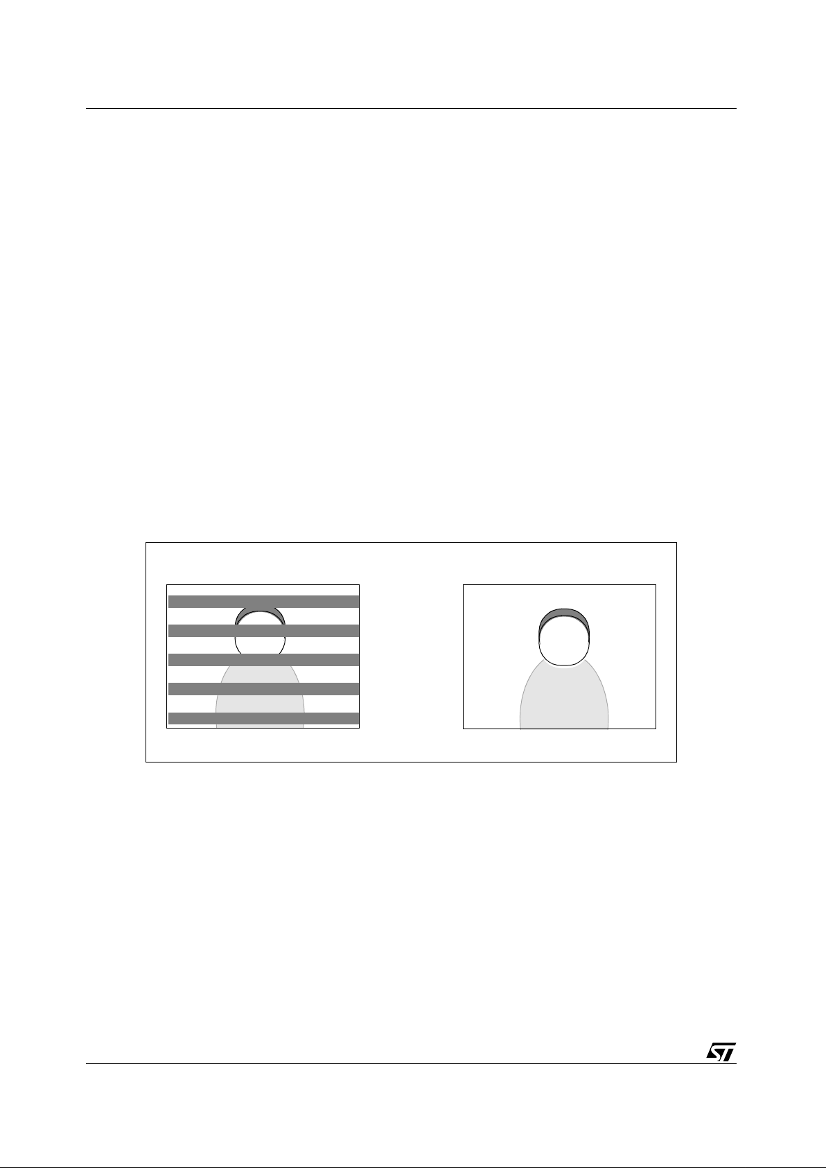
Figure 2: Illustration of flicker problem
Flicker setting not correct Flicker setting correct
Page 15

ADCS 7283313C 15/44
STV0681 Camera Modes of Operation
3 Camera Modes of Operation
This section refers to the two switches as discussed in section
Section 2.2.1
● “Mode”: connects GPIO0 pin of STV0681 to GND when pressed
● “Shutter”: connects GPIO1 pin of STV0681 to GND when pressed
Pressing the mode switch repeatedly cycles through a series of modes as displayed on the LCD.
When a given mode is displa yed it may be selected b y pressing the shutter b utton. If an optio n is not
selected within 5 seconds, the display reverts to showing the number of available pictures.
3.1 Modes available
Figure 3: STV0681 modes (CIF camera with 16Mbit SDRAM assumed)
Normal: 20 / 80
Audio Record: Ar
Audio Playback: AP
Delete Last: dA / dP / dC
Continuous Capture: Ct
Self-Timer:St
Clear All: CL
Resolution: Hr / Lr
Notes:
1. AudioRecord onlyavailable if audio hardw are isfitted
2. AudioPlayback onlyavailable once an audio clip has been recorded
3. DeleteLast displays (only available if audio hardware fitted)
dA - if the las t object isan audio clip
dP - if the last objectisa picture
dC - if the last object is a continuouscaptureclip
Themodeisinhibitedifthecameraisempty.
4. ContinuousCapture mode is inhibited when the flashgun isenabled
(SW 6down)
Press Mode button
After 30sec of inactivity
Standby mode(untethered)
Page 16

Camera Modes of Operation STV0681
16/44 ADCS 7283313C
3.2 Description of modes
3.2.1 Standby mode (untethered) and Wake-up
On power-up, or wake-up from untethered standby mode, (i.e. by pressing the Mode button), the
camera beeps twice. The LCD briefly indicates the camera resolution either ‘Hr.’ for high resolution
(80 CIF or 26 V GA images - usin g 64M bit memory) or ‘Lr’ for lo w r esol ution ( 322 QC IF or 1 07 VGA
images - using 64Mbit memory) and then displays the number of pictures which may be taken.
Please note that in lo w resolution m ode, althoug h there can be up to 322 imag es av ailab le, the LCD
counter only goes up to 99, it reports 99 until there are less than 99 images left.
The camera goes back to standby mode after 30 seconds of i nactivity, LED1 turns off and the LCD
goes blank. This is also achieved by pressing the mode switch during more than 2 seconds.
3.2.2 Normal mode
Press the shutter button to take a picture . The camera beeps . A high pitched beep indicates that the
picture was taken successfully and the counter decrem ent s (if ther e ar e less than 99 images lef t to
take). A low beep indicates insufficient light to take a picture. A series of beeps indicates that the
camera is full.
Stored pictures can be uploaded to a PC at any time , whether or not the camera is full. Plugg ing the
USB connector into the camera causes it to reset and issues a double beep but all stored pictures
remain. When the USB connector is unplugged the camera goes to sleep. When connected to the
PC, the camera can still be used in the normal way.
Note: When flashgun is enabled, the camera always takes a picture, with or without sufficient light.
3.2.3 Audio record - Ar
This mode is available with audio record hardware fitted.
Pressing the shutter button within 5 seconds causes the camera to start recording for as long as the
shutter button is pressed down. If the shutter button is not pressed within 5 seconds, the camera
reverts to normal picture taking mode. Whilst recording, the LCD display flashes ‘Ar’. If the
recording stops because the memory is full, the ‘memory full’ audi o tone is sounded and the displ ay
stops flashing and displays ‘00’. The audio data is digitized and stored in SDRAM.
3.2.4 Audio Playback - AP
This mode is available with audio playback hardware fitted.
Pressing the shutter button within 5 seconds causes th e camera to pla y ba c k the m ost recent audio
recording. If the shutter button is not pressed wit hin 5 seconds the camera re v erts to normal picture
taking mode. Whilst playing, the LCD display flashes ‘AP’.
Once in Audio Playback mode, repeated presses of the shutter button steps the camera through
each of the audio recordings in the camera (most recent first). Keeping the shutter button pressed
down also allows to cycle through the audio recordings. Pressing the mode button during playback
stops the audio clip.
Note: Minimum audio recording length is set to 0.5 seconds.
Page 17

ADCS 7283313C 17/44
STV0681 Camera Modes of Operation
3.2.5 Delete Last Object - dA/dP/dC
This mode is available with audio record hardware fitted.
If the last object captured was an audio recording, 'dA' (delete audio) is displayed, if the last object
was an image, then 'dP' (delete picture) is displayed, or, if the last object was part of a continuous
capture sequence, then 'dC' (delete continuous) is displayed. If the camera is empty, the mode is
suppressed. The mode works like ‘CL’ (Clear All), that is once the mode is selected, pressing the
shutter button once causes the camera to beep and ‘dA’, ‘dP’ or ‘dC’ to start flashing. Pressing the
shutter button again within 5 seconds deletes the last audio clip, picture or continuous capture
sequence.
3.2.6 Continuous mode - Ct
Pressing the shutter button within 5 seconds causes the camera to start taking pictures for as long
as the shutter button is p ressed down (and the camera is not full). If the shutter b utton is not pressed
within 5 seconds the camera reverts to normal picture taking mode.
Note: 1 In continuous mode, the camera allows pictures to be taken regardless of the available light, which
could result in insufficient exposure.
2 In continuous mode, only e very alternate field is gr abbed hence capture rate is h alved. For exam ple,
12.5fps CIF and 7.5fps VGA
3 Continuous mode is suppressed when the FlashGun enable signal (GPIO2) is high.
3.2.7 Self timer - St
Pressing the shutter button starts a 10-second self-timer. The camera issues a short beep every
second, follow ed b y a longer beep. A further beep will then indicate that the picture has been taken
(high beep - picture successful, low beep - insuffi cient light, picture not tak en) . The self-timer mode
cannot be selected when the camera is full. The self-timer count down cannot be stopped once it
has started.
3.2.8 Clearing the camera memory - CL
Pressing the shutter button once cause s the camer a to beep and the ‘CL’ to start flashing. Pressing
the shutter button again within 5 seconds clears all the image s/audio clips in the camera and r esets
the counter.
3.2.9 Changing picture resolution - Hr/Lr
The resolution option is displayed, either Hr to change to high-resolution mode (if currently in lowresolution mode) or Lr to change to low-resolution (if currently in high-resolution mode). Press the
shutter button within 5 seconds to sel ect th e r esoluti on o ption, the cam er a bee ps and the di spl ay is
reset, indicating the number of pictures available in the new mode. The picture resolution can be
changed at any time, that is the camera can store both high and low resolution images.
Page 18

STV0681 Hardware Interfaces STV0681
18/44 ADCS 7283313C
4 STV0681 Hard ware Interfaces
4.1 Sensor interface
STV0681 uses a standard ST digital interface from the sensor, and the sensor clock input is
provided by an output from STV0681. The design of a camera using this chipset should be
implemented as closely as possible to the reference design (
Chapter 7
), in which case the chipset
can be regarded as a functional ‘black box’, and no further details regarding the STV0681-sensor
interface are required.
4.2 Memory interface
STV0681 is designed to interface to an external 16Mbit or 64Mbit SDRAM (see
Table 1
). The
SDRAM device must have a 16 bit wide data bus and operate from a 3.3V supply. Two sizes of
SDRAM memory are supported by STV0681, 16MBits (1M x 16 bits wide) or 64MBits (4M x 16 bi ts
wide), the memory size is auto-detected by STV0681. STV0681 clocks the SDRAM at 6MHz,
typically this is well below the figures offered by most manufacturers’ devices.
4.2.1 SDRAM current consumption
For maximum system battery life while no pictures are being taken, and to meet requirements for
USB compliance, an SDRAM should be chosen with the lowest possible self refresh current
specification.
In addition, the USB suspend mode current specification requires that the camera consumes less
than 300µA when un-tethered. Meeting this specification, which is included in the requirements for
USB compliance, assumes an SDRAM with up to appro x imatel y 250µA self-refresh curr ent, based
on a current consumption of approximately 50µA for STV0681 + support circuit.
Page 19

ADCS 7283313C 19/44
STV0681 STV0681 Hardware Interfaces
4.2.2 SDRAM interface timing requirements
Figure 4: SDRAM Read Timing (16Mbit device, burst read)
DCLK
Command
DQM
A0-9,BA
A10
ACTIVE
READ
NOP PRECHARGE NOP
ROW COLUMN
ROW
DOUT M
DOUT M + 1 DOUT M + 2 DOUT M + 3
DQ
READ Latency
t
CK
t
RCD
t
RC
CKE
t
RAS
DQ sample DQ sample DQ sample DQsample
t
RP
t
CMS
t
CMH
t
AS
t
AH
t
L
t
H
t
CMS
t
CMH
t
AC
t
OH
Page 20

STV0681 Hardware Interfaces STV0681
20/44 ADCS 7283313C
4.2.3 SDRAM refresh period
The SDRAM refresh period from STV0681 is guaranteed to be inferior or equal to 15.6µs during
‘Snapshot’/self-timer/continuous/tethered video modes of operation (that is not standby mode). In
standby mode, the SDRAM is set to self-refresh, therefore no refresh from STV0681 takes place.
4.2.4 SDRAM initialisation period
The SDRAM initialisation period is currently set to 981µs in STV0681.
Figure 5: SDRAM Write Timing (16Mbit device, burst write)
Table 3: Timing parameters for SDRAM read/write
Symbol Min. Max Units Symbol Min. Max Units
t
CK
166.45 166.89 ns t
DS
81.01 ns
t
CH
½tCKt
DH
83.41 ns
t
CL
½tCKt
RCD
1t
CK
t
AC
½t
CK
t
RAS
55t
CK
t
OH
0nst
RC
7t
CK
t
CMS
82.88 ns t
RP
2t
CK
t
CMH
82.85 ns t
RCD
1t
CK
t
AS
82.88 ns t
AH
82.76 ns
DCLK
Command
DQM
A0-9,BA
A10
ACTIVE
WRITE
NOP PRECHARGE NOP
ROW COLUMN
ROW
DIN M
DIN M + 1 DIN M + 2 DINM + 3
DQ
t
CK
t
RCD
t
RC
CKE
t
RAS
t
RP
t
CMS
t
CMH
t
AS
t
AH
t
L
t
H
t
CMS
t
CMH
t
DS
t
DH
Page 21

ADCS 7283313C 21/44
STV0681 STV0681 Hardware Interfaces
4.3 USB interface
STV0681 includes a USB Version 1.1 compliant Universal Serial Bus Interface, including a
transceiver. This allows direct connection from STV0681 to a USB connector with minimal
additional hardware (that is a small number of passive discretes) - see
Chapter 7
The USB interface interfaces the STV0681 to the USB at full speed 12MHz data rate. Some of the
features are:
● Compliant with USB protocol revision 1.1.
● USB protocol handling.
● USB device state handling.
● Clock and data recovery from USB.
● Bit stripping and bit stuffing functions.
● CRC5 checking, CRC16 generation and checking.
● Serial to parallel conversion.
● Single bulk-end point.
USB drivers are supplied by ST. For USB timing information, please refer to the USB specification
V1.1.
Page 22

STV0681 Hardware Interfaces STV0681
22/44 ADCS 7283313C
4.4 UART module for RS232 interface
The UART module on STV0681 provides a 115200 baud full duplex serial interface to an external
host.
4.4.1 RS232 physical interface
STV0681 does not support direct connection to a RS232 serial link. Physical line driver circuitry is
required, e.g. using a standard RS232 transceiver chip, or by using a small number of low cost
discretes (refer to Ref erence Design for details). Unscreened cab le can be used, a suitab le low cost
connector is a 3.5mm stereo audio jack plug.
4.4.2 UART module overview
Receiving data
The UAR T modu le in STV0681 receives serial data through the RXD pin. Data r eception is initi ated
by a 1-to-0 transition on RXD, and the received data is sampled every 8.66µs.
If the RXD input is not 0 when the incoming data is first sampled, the UART module goes back to
look for another 1-to-0 transition. This is to provide rejection of false start bits. If the start bit proves
valid, reception of the rest of the frame proceeds.
Transmitting data
When a transmission is activ ated b y STV0681, the conten ts of an i nternal transmit shift re gister are
shifted onto the TXD pin, every 8.66µs.
The UAR T oper ates at 12MHz, w hich is not an integer multip le of 115200 , so the actual b aud rate is
115232 +/- 0.3%, which is well within the requirements of a typical 16x oversampling UART, which
can tolerate a 3.75% error in baud rate.
Page 23

ADCS 7283313C 23/44
STV0681 STV0681 Hardware Interfaces
4.5 Po wer manage ment and battery type
STV0681 and the SDRAM requir e a 3.3V supply. When a VV6411 or VV6501 (3.3V) sensor is used,
a single voltage regulator can regulate the supply for all three components from the battery, or the
sensor on-board VReg can be used. These are explained more fully in the reference design.
4.5.1 Power switching to USB
Included in the USB compliance requirements , is the abili ty of the camera to report to the PC when
connected to the USB bus, whet he r or no t there is a fresh battery in the camera. This means that
power sourcing from USB is required, which also saves on battery life while the camera is used in
USB tethered video mode. In order to allow switching from battery to USB power, some additional
hardware is required.
● The USBDETECT input to STV0681 is used to detect that a USB power supply is connected
● If the USB is detected, additional hardware is used to switch off the battery
● An inrush protection circuit can protect the USB bus from current draw in the case of a low battery/
battery not fitted. This may be necessary to comply with the USB specification.
For precise USB compliance requirements, please consult the USB specification version 1.1.
4.5.2 Switched sensor supply
Dependant on the hardware implementation, the SENSPWR output from STV0681 is used to put
the sensor into suspend mode. This has a significant improvement on battery life.
4.5.3 Battery type
It is possible to use v arious battery types and configurations . Th e e v aluati on kit uses four 1.5V AAA
cells.
Page 24

STV0681 Hardware Interfaces STV0681
24/44 ADCS 7283313C
4.6 Quartz crystal
Regardless of the sensor type or anti-f licker requirements , t he sensor + STV0681 chi pset ope r ates
from a single 12MHz fundamental quartz crystal. For specification requirements, see
Table 13
.
STV0681 includes an on-chip low jitter PLL. For PLL characteristics, see
Table 12
.
4.7 Numeric LCD interface
STV0681 supports a 2-digit LCD panel only, for alpha-numeric display.
4.7.1 LCD types
STV0681 connects to a non multiple xed, dir ect drive LCD with 2 x 7 segments . Many LCD types ar e
compatible with this interface. The LCD refresh frequency is 34.7Hz.
4.7.2 LCD interface pinout
The convention for segment numbering is as follows: '0' connects to segment 'a', '1' connects to
segment 'b', and so on, where a to g are standard for all 7-segment displays, as well as an LCD
common output, giving fifteen signals in total.
Page 25

ADCS 7283313C 25/44
STV0681 STV0681 Hardware Interfaces
4.8 Switches and LED’s
The GPIO lines on STV0681 have the following pre-defined functions, see
Section 2.2
for user
interface functionality.
MODE push button and SHUTTER push button: GPIO0 and GPIO1: both push button inputs have
internal de-bounce circuits, reducing the amount of hardware required externally. It is
recommended that labelling is used on the camera casing to help the user understand the
functioning of the 2-button interface.
4.8.1 Input to select between 50 and 60Hz flicker frequency: GPIO3
This allows for factory setting of the anti-flicker frequency, dependant on the final country of
destination. See also
Section 2.6
. The polarity of this selection is detailed in the reference design.
4.8.2 LED indicator output: GPIO5
The LED output has an 8mA current sinking capability.
4.8.3 Other pins: GPIO2, 4, 6, 7
With STV0681, these pins are used, as detailed in
Table 4
.
Their specific functions are detailed in the reference design and in the following documents
available from ST:
● Audio: application note AN1310
● Flashgun: application note AN1312
4.8.4 Audio Record Hardware interface
STV0681 implements the A/D conversion by outputting successive analogue levels (successive
approximation) through the DAC output, which are compared with the actual signal level (output
from the sensor microphone pr eampl ifi er), and the resulting high or lo w si gnal fr om the comp ar ator
is read at GPIO4. The sampl ing frequ ency is 11kHz, an d the successive appro ximation is done at 8
bits resolution per sample. It is not po ssible to speed up the sampling frequency due to the limitation
of STV0681 processing speed.
An actual hardware implementation is given in the audio application note AN1310.
4.8.5 Audio Playback Hardware interface
STV0681 outputs the desired signal lev el through th e D A C output, which is amplified to the speak er
or headphone socket . GPIO6 is used to switch o ff the amplifi er during periods of audio record ing, to
prevent th e succe ssive approximation waveform from being heard during periods of recording, and
to reduce the power consumption and unwanted crackle through the speaker.
An actual hardware implementation is given in the audio application note AN1310.
Table 4: Other GPIO usage with STV0681
GPIO 2 4 6 7
Audio Record No Yes No No
Audio
Playback
No No Yes No
Flashgun Yes No No Yes
Page 26

STV0681 Hardware Interfaces STV0681
26/44 ADCS 7283313C
4.9 Flashgun hardware interface
STV0681 will revert to flashgun exposure when it detects GPIO2 is high. Ideally the hardware
should combine the two factors of (a) user intentio n (e .g. user s wi tches on fl ashgun) an d (b) char ge
sensing (i.e. flash is charged up and ready to fire).
These two factors (a) and (b) are independent, since there may be a delay of several seconds
between switching on the flashgun charger , and the fla shgun being abl e to fire. To revert to flashgun
exposure before the flashgun is completely charged up would cause very bad pictures to be taken
in low light conditi on s because ther e i s n o “ low light” threshold when flashgun exposure is e nabled,
since the camera expects a flash to fire. A suggested flashgun hardware interface is given in the
flashgun application note AN1312.
When flashgun exposure is enabled and the shutter button is pressed, a picture is taken and the
flash trigger pin GPIO7 is pulsed low at the correct point in time so that all l ines of the CMOS imager
are exposed.
4.10 IR filter
An Infra-Red Blocking Filter is required to achieve correct colour response. The exact specification
for the IR filter characteristics are given in the reference design manual.
Page 27

ADCS 7283313C 27/44
STV0681 Customising the STV0681
5 Customising the STV0681
The firmware inside the STV0681 is stored in ROM and may not be changed. It is possible,
however, to use an external serial EEPROM to store certain information to allow a degree of
customization of the device.
The STV0681 reports a USB Vendor ID (VID) of 0553(hex) and a Product ID (PID) of 0202 (hex).
Alternative values f or th e VID and PID as well as Man ufactur er and Product strings ma y be stored in
an external EEPROM.
In addition to USB descriptor information, the EEPROM may also be used to set various other
parameters as follows:
● Auto power-down time: this is the length of time before the STV0681 shuts down after no activity.
● Mode button power-down time: the length of time you must hold the Mode button to powerdown the
system.
● 50Hz/60Hz flicker-free selection: the EEPROM allows this selection to be via a GPIO pin on the
STV0681 or fixed at either 50Hz or 60Hz
● Number of self-timer beeps
5.1 External EEPROM
An external 128byte serial EEPROM may be used in conjunction with STV0681 to hold customer
specific information.
The EEPROM is connected onto the sensor IIC bus and must be set to IIC address A0 (hex). The
EEPROM is auto-detected by the STV0681 and no additional changes need to be made . A suitable
EEPROM device is manufactured by STMicroelectronics part number M24C01W (alternatives are
available from other suppliers).
Page 28

Customising the STV0681 STV0681
28/44 ADCS 7283313C
5.2 EEPROM data format
5.3 Programming the EEPROM
There is no facility to program the EEPROM using the STV0681 itself and so the device must be
programmed before fitting it to the PCB.
Location(decimal) Contents
0 Leave blank
1 VidLo, The low byte of the Vendor ID
2 VidHi, The high byte of the Vendor ID
3 PidLo, The low byte of the Product ID
4 PidHi, The high byte of the Product ID
5 Max Power (in units of 0.5mA)
6 Max Power with audio playback enabled (in units of 0.5mA)
7 Auto powerdown time Hi byte (in units of 256ms)
8 Auto powerdown time Lo byte (in units of 10ms)
9 Mode button press time Hi byte (in units of 256ms)
10 Mode button presss time Lo byte (in units of 10ms)
11 50Hz/60Hz flicker free selection
0 = board link (GPIO3) , 1 = 50Hz, 2 = 60Hz
12 Number of self-timer beeps
13 CheckSum - low byte of sum of EEPROM locations 1 to 12
inclusive.
20 Length of Manufacturer String
21-54 (max) Manufacturer String (ASCII codes)
55 Length of Product String
56-89 (max) Product String (ASCII codes)
90 Length of Interface0 String
91-127 (max) Interface 0 String (ASCII codes)
Page 29

ADCS 7283313C 29/44
STV0681 Software support
6 Software support
6.1 General features
The chipset is a dual-mode camera, i.e. stills and video, and is supported by a range of
demonstration software, standard drivers, and software development options.
PC
Driver software is available to support both USB and RS232 interfaces. Drivers are available for
TWAIN, WIA, Video for Windows (VfW) and DirectShow (DS) depending on the Operating System
as listed below:
● Win98/Win98SE/WinME – VfW and TWAIN
● Win2k – DS, VfW and TWAIN
● WinXP – DS, VfW, WIA and TWAIN
Mac
Quicktime drivers and a Photoshop stills plug in for MacOS 8.6/9.0/9.1/9.2 are supported.
The driver will also run under MacOS X in Classic Mode.
Example software applications (PC only) are provided to create. AVI video files from untethered
continuous capture of images (AVICreator), to upload still images and recorded sounds
(LCDCdemo) and to do wnload .WA V fi les f rom the PC to th e camera (CustomSound) . In each case,
PC source code is provided to assist in OEM software development using the SDK.
ST colour processing and defect detection/correction software runs on the host and is supplied
under licence agreement as part of all host software/drivers/SDK
6.1.1 Still image upload
This is available through demonstration softw ar e , OEM custom software, or using standard TWAIN
applications. Features include:
● Fast upload through USB, or upload through RS232.
● Colour display of image thumbnails for picture selection.
● Download of full image once selected by user software.
● Automatic detection and correction of sensor defects
● Colour processing of full image, using the ST colour process
The above fe atur es also apply to “AVI Creator” or any OEM custom software for AVI video creation
at part of pictures taken while un-tethered, since this is essentially a “stills” function.
6.1.2 Streaming video (only while tethered to USB)
This is available through demonstration software, or using standard VfW applications. Features
include:
● Streaming video through standard VfW driver
● Automatic detection and correction of sensor defects
● Colour processing of full image, using the ST colour process
Page 30

Software support STV0681
30/44 ADCS 7283313C
6.2 Software installation
The following software support is only available to OEMs. Access to the latest installation files is
possible through a passw ord-protected web page , contact ST for detai ls. The installatio n files are for
the following:
● Drivers (always check the Web site for latest driver version).
● EVK software, i.e. LCDCdemo.exe and AVIcreator.exe, G2Video.exe, and CTItest2.exe
● SDK installation: source code for sample applications, and documentation
6.2.1 Driver support available
6.2.2 EVK software
Note: The following is also su pplied wi th e v alu ation kits/de monstrati on units , b ut all the following software
is only for demonstration purposes and should NOT be supplied as an end-user product. However,
application-level source code (i.e. not driver/colour processing source) for LCDCdemo.exe, AVI
creator, and CTItest.exe is a vailable as part of the SDK, wh ich allo ws si mila r applicati ons to be b uilt
by the software developer:
1 Simple demonstration software LCDCdemo.exe for uploading thumbnails and images.
2 AVIcreator.exe software for uploading continuous images for creating ‘movie’ clips.
3 G2Video.exe is a VfW application which shows streaming video while tethered to USB and
allows creation of.AVI video clips.
4 CTItest.exe is only for debugging purposes, for software developers using the SDK
6.2.3 Software Development Kit (SDK) and source code
A software development kit allows the OEM to develop a custom application which calls the same
range of drivers as listed in
Section 6.2.1
, hence allowing the OEM application to perform picture
download, thumbnail display, and colour processing using the ST colour process. Inclusion of
source code for the applications listed in
Section 6.2.2
allows the software developer to use these
as the basis for their own application.
The SDK is supplied by ST as a 32-bit DLL f ormat, running on Microsoft Windows 98/Wi n2K
TM
, and
accessed through a documented software interface. Development requires Microsoft Visual Studio
Version 6 or later. This provides the basis for developing a custom software application for stills.
Note: Source code for PC Drivers, Defect Correction and Colour Processing algorithms are not available.
Table 5: Driver choices
Interface type:
RS232 USB
PC Operating system
Microsoft Windows
:
Win9x, WinNT4, Win2k,
Windows Millennium
Windows XP
Microsoft Windows:
Win98 and Win2k only,
Windows millenium
Windows XP
Mac OS
N/A 8.6, 9.0, 9.1, 9.2
Page 31

ADCS 7283313C 31/44
STV0681 Detailed Chipset Specifications
7 Detailed Chipset Specifications
7.1 Typical camera specifications
The following data assumes that the camera has been built according to the ST Reference Design.
Dual USB or battery power supply is only possible when the required power switching hardware is
included.
Figures are approximate and depend on actual components sources.
7.2 Absolute max imum ratings
T ab le 6: Typical camera specifications
Supply voltage
4.1-6V (when powered from battery or USB)
Operating temperature range
0oC - 40oC
Max. RS232 cable length supported
2m
CIF output
352 x 288 pixels
QCIF output
176 x 144 pixels
VGA output
640 x 480 pixels
QVGA output
320 x 240 pixels
SDRAM storage and image upload format
Raw Bayer
PC driver output format
Colour RGB bitmap
Table 7: Approximate shutter speeds
Sensor resolution Min. Max
CIF 8 µs44ms
VGA 8 µs 66 ms
Table 8: STV0681 absolute maximum ratings
Parameter Range Units
Ambient temperature 0 to 40 °C
Storage temperature -50 to 150 °C
Voltage on USB D+/D- 0-VDD V
Page 32

Detailed Chipset Specifications STV0681
32/44 ADCS 7283313C
7.3 STV0681 specifications
7.4 USB specifications
Note: 1 VDI = |(D+) - (D-)|
2V
CM
includes VDI range.
3TF
RFM
=(TFR / TFF).
4Z
DRV
includes an external resistor of 20 Ohms serial to this transceiver.
Table 9: STV0681 specifications
Parameter Min. Typ. Max. Units
Supply voltage 3.0 3.3 3.6 V
Current consumpti on (normal operation ) 18 - mA
Stand-by current consumption - 10 - µA
Package 100TQFP (14x14 x1.4)
Exposure control 1 000 000: 1
Table 10: STV0681 USB specifications
Parameter Description Min. Typ. Max. Units Notes
VDD Power Supply 3.0 3.3 3.6 V
V
ILU
USB differential pad D+/D- input low 0.8 V
V
IHU
USB differential pad D+/D- input hig h (d riven) 2.0 V
V
IHUZ
USB differential pad D+/D- input high (floating) 2.7 3.6 V
V
DI
USB differential pad D+/D- input sensitivity 0.2 V 1
V
CM
USB differential pad D+/D- common mode voltage 0.8 2.5 V 2
V
OLU
USB different i al pa d D+/D- output low voltage 0.0 0.3 V
V
OHU
USB different i al pa d D+/D- output high volta ge 2.8 3.6 V
V
CRS
USB differential pad D+/D- output signal cross over
voltage
1.51 1.79 V
R
PU
USB differential pad D+/D- pull up resistor 1.425 1.575 kΩ
R
PD
USB differential pad D+/D- pull-down resistor 14.25 15.75 kΩ
TF
R
Rise Time 4 20 ns
TF
F
Fall Time 4 20 n s
TF
RFM
Differential Rise Time and Fall Time Matching 96 98 %
Note 3
Z
DRV
Driver Output Resistance 24.7 26.6 30.0 Ω
Note 4
Page 33

ADCS 7283313C 33/44
STV0681 Detailed Chipset Specifications
7.5 DC characteristics
7.6 PLL characte ristics
7.7 Crystal tolerance
Table 11: STV0681 DC characteristics
Parameter Description Min. Typ. Max. Units
V
II
CMOS input low voltage 0.35 VDD V
V
IH
CMOS input high voltage 0.65 VDD V
V
T+
CMOS schmi tt input low to high threshold voltage 2.15 V
V
T-
CMOS schmitt input high to low threshold voltage 1.05 V
V
T
Threshold point 1.65 V
V
OH
Output high voltage 2.4 V
V
OL
Output low voltage 0.4 V
T ab le 12: STV0681 PLL char a cteristics
Parameter Conditions Symbol Min. Typ. Max. Unit
Peak to peak jitters @VCOfreq = 240MHz - 312MHz -- -- -- 500 ps
Duty cycle -- 45 50 55 %
Operating voltage range VDD 3 3.3 3.6 V
Input low volt a ge VDD= 3 .3V VIL - 0.8 V
Input high voltage VDD=3.3V VIH 0.7VDD VDD V
Pull in Time + Locking Time Ready -- -- 0.1 ms
Output Slew Rate CL: Output Load (pF) Tsr(Fout) -- 0.100+0.1082*CL -- ns
Table 13: STV0681 crystal tolerance
Parameter Min. Typ. Max. Units
Crystal specification 50/50/10/30 (12mhz Fundamental)
Crystal frequency 12.000 MHz
Frequency tolerance 50 ppm
Temperature stability 50 ppm
Operating temperature -10 °C
Page 34

Detailed Chipset Specifications STV0681
34/44 ADCS 7283313C
7.8 Typical current consumption of complete camera
The following data assumes that the camera has been built according to reference design referred
to in
Chapter 10
. Figures are approximate and depend on actual components sources - see notes.
The sensor operates at @ 3.3V DC
Note: 1 See Table 9 from Section 7.3
2 From limited evaluation, typical self-refresh current figures of certain SDRAM chips are well below
manufacturers’ maximum specification,
e.g. 100-250µA
.
3 Option included in reference design to save current consumption, which can increase battery life
and increase chances of meeting USB suspend mode compliance requirements.
Table 14: Current consumption, complete STV0681+VV6411/ 650 1 camera
Mode Typical Comments
’Snapshot’/Continuous/
Self timer mode
(while un-tethered)
60mA Assuming appropriate hardware include d, powe r is sour ced
from PC while USB connected.
’Snapshot’/Continuous/
Self timer mode
(while tethered to PC)
60mA
While playing back audio
sounds thro ugh speaker
90mA
Assuming 8
Ω speaker as explained in application note
AN1310
Standby mode
(when NOT connected to
USB)
Approx. 270µA + SDRAM
self-refresh current
(see
Note 2
) + sensor
suspend mode current
Total current in this mode equals
:
STV0681 standby current consumption ( see
Note 1
)
+ SDRAM self-refresh current (see
Note 2
)
+ peripheral circ uitry (approx. 50
µA).
+ Sensor suspend mode current
PC Suspend mode
(when connected to USB):
Sensor SUSPEND pin
asserted
Approx. 300µA + SDRAM
self-refresh current
(see
Note 2
) + sensor
suspend mode current
Total current in this mode equals
:
STV0681 Stan dby current consumption (see
Note 1
)
+SDRAM self-refresh current (see
Note 2
)
+ peripheral circ uitry (approx. 50
µA)
+ 200
µA, based on 1.5k pull-up in camera and 15k pull-
down in PC.
+ Sensor suspend mode current
Standby mode
(when not connected to
USB): senso r powered off
using FET (see
Note 3
)
Approx. 270µA + SDRAM
self-refresh current
(see
Note 2
)
Total current in this mode equals
:
STV0681 Stan dby current consumption (see
Note 1
)
+SDRAM self-refresh current (see
Note 2
)
+ peripheral circ uitry (approx. 50
µA).
PC Suspend mode
(when connected to USB):
sensor powered of f using
FET (see
Note 3
)
Approx. 100µA + SDRAM
self-refresh current
(see
Note 2
)
Total current in this mode equals
:
STV0681 Stan dby current consumption (see
Note 1
)
+SDRAM self-refresh current (see
Note 2
)
+ peripheral circ uitry (approx. 50
µA).
Page 35

ADCS 7283313C 35/44
STV0681 STV0681 pin description
8 STV0681 pin description
8.1 STV0681 pinout
Figure 6: STV0681 pinout diagram
12345678910111213141516171819202122232425
7574737271
70
69686766656463626160595857565554535251
76
77
78
79
80
81
82
83
84
85
86
87
88
89
90
91
92
93
94
95
96
97
98
99
100
50
49
48
47
46
45
44
43
42
41
40
39
38
37
36
35
34
33
32
31
30
29
28
27
26
STV0681
TQFP100
DQ_15
DQ_1
DQ_14
DQ_2
DQ_13
DQ_3
DQ_12
DQ_4
DQ_11
DQ_5
VDD
VSS
DQ_10
DQ_6
DQ_9
DQ_7
DQ_8
DQML
WE
DQMU
CAS
DCLK
RAS
CKE
CS
RESET
XOUT
XIN
TEST2
TEST1
TEST0
USBUSB+
USB_DET
AD_4
AD_3
VDD
VSS
AD_5
AD_2
AD_6
AD_1
AD_7
AD_0
AD_8
AD_10
AD_9
AD_13
AD_11
AD_12
MODE
SHUTTER
FLASH_EN
50/60
COMP_OUT
VSS
VDD
LED
AMP_EN
FL_TRIG
SENSPWR
SENSRST
SENS_CLK
QCLK
SD[0]
SD[1]
SD[2]
SD[3]
SDA
SCL
RXD
TXD
PLL_GVSS
PLL_AVSS
PLL_AVDD
AUD_VSS
LO_BAT_REF
LO_BAT
DACRES
DACOUT
AUD_VDD
PIEZO
LCD_COM
VSS
VDD
LCD2_6
LCD2_5
LCD2_4
LCD2_3
LCD2_2
LCD2_1
LCD2_0
LCD1_6
LCD1_5
LCD1_4
LCD1_3
LCD1_2
LCD1_1
LCD1_0
DQ_0
Page 36

STV0681 pin description STV0681
36/44 ADCS 7283313C
8.2 STV0681 pin description
Table 15: STV0681 pin listing
Pin no. Signal Type Description drive
Sensor Interface
65 SENSPWR Output, active
high
Power-up Sensor 2mA
(SL)
64 SENSRST Output, active low Reset Sensor 2mA
(SL)
56 SCL Input/Output
(OD,T)
Sensor serial interface 4mA
(SL)
57 SDA Input/Output
(OD,T)
Sensor serial interface 4mA
(SL)
58 SD[3] Input (S,T) Sensor data
59 SD[2] Input (S,T) Sensor data
60 SD[1] Input (S,T) Sensor data
61 SD[0] Input (S,T) Sensor data
62 QCLK Input (S,T) Qualification clock from sensor
63 SENS_CLK Output Clock output to sensor 4mA
I/O and Camera Control pins
75 M ODE Debo unced input Push butto n (Wake-up/ M ode)
74 S HUTTER Debounced input Push button (Sh utter/Confirm)
73 FLASH_EN Input Enable Flash Exposure (Active High)
72 50/60_SEL Input S elect be tween 50Hz and 60Hz lighting
71 COMP_OUT Input Output from Audio Comparator
68 LED Output (OD) LED indicator 8mA
(SL)
67 AMP_ENABLE Output, active lo w
(OD)
Audio Amplifier Enable 8mA
(SL)
66 FL_TRIG Output, active low
(OD)
Flashgun trigger 8mA
(SL)
USB Interface
42 USBDET Input (S) Detect Power source from USB.
(For camera with RS232 only, this pin should be tied
to GND)
USB
specific
ation
V1.1
complia
nt I/O
43 DATA+ Input/Outp ut US B bu s
(For camera with RS232 only, this pin should be
connected to test points to allow for USB production
test (lens focussing))
44 DATA- Input/Output USB bu s.
(For camera with RS232 only, this pin should be
connected to test points to allow for USB production
test (lens focussing))
Page 37

ADCS 7283313C 37/44
STV0681 STV0681 pin description
RS232 Interface
54 TXD Output Serial data transmit
(For camera with USB only, this pin should be tied to
RXD)
4mA
(SL)
55 RXD Input (S) Serial data receive
(For camera with USB only, this pin should be tied to
TXD)
STV0680B Master Clocks and Reset
48 XIN Input Quartz Crystal IN
49 XOUT Output Quartz Crystal OUT
50 RESET Input (S) Active (LOW) STV0680B reset
System Memory (SDRAM) Interface
20 DQMU Output Data input/output mask for dram_DQ[15:8] 2mA
(SL)
22 DCLK Output Clock: all SDRAM input signals are sampled on the
positive ed ge
4mA
(SL)
24 CKE Output Clock enable: activates (HIGH) and deactivates
(LOW) the SDRAM CLK signal
2mA
(SL)
32 AD0 Output SDRAM address A0 2mA
(SL)
34 AD1 Output SDRAM address A1 2mA
(SL)
36 AD2 Output SDRAM address A2 2mA
(SL)
40 AD3 Output SDRAM address A3 2mA
(SL)
41 AD4 Output SDRAM address A4 2mA
(SL)
37 AD5 Output SDRAM address A5 2mA
(SL)
35 AD6 Output SDRAM address A6 2mA
(SL)
33 AD7 Output SDRAM address A7 2mA
(SL)
31 AD8 Output SDRAM address A8 2mA
(SL)
29 AD9 Output SDRAM address A9 2mA
(SL)
30 AD10 Output SDRAM address A10 2mA
(SL)
27 AD11 Output SDRAM address A11 f or 64M S DRAM or B A for 16M
SDRAM
2mA
(SL)
26 AD12 Output SDRAM address A12, BA0 for 64M SDRAM, unused
on 16M
2mA
(SL)
Table 15: STV0681 pin listing
Pin no. Signal Type Description drive
Page 38

STV0681 pin description STV0681
38/44 ADCS 7283313C
28 AD13 Output SDRAM address A13, BA1 for 64M SDRAM, unused
on 16M
2mA
(SL)
25 CS Output, active low Chip select: enables (registered LOW) and disables
(registered HIGH) the SDRAM comman d decoder.
2mA
(SL)
23 RAS Output, active low SDRAM row address strobe command 2mA
(SL)
21 CAS Output, active low SDRAM column address strobe command 2mA
(SL)
19 WE Output, active low SDRAM wr i te enable command 2mA
(SL)
18 DQML Output Data input/output mask for dram_DQ[7:0] 2mA
(SL)
100 DQ0 Input/Output SDRAM Data Bus 2mA
(SL)
2 DQ1 Input/Output SDRAM Data Bus 2mA
(SL)
4 DQ2 Input/Output SDRAM Data Bus 2mA
(SL)
6 DQ3 Input/Output SDRAM Data Bus 2mA
(SL)
8 DQ4 Input/Output SDRAM Data Bus 2mA
(SL)
10 DQ5 Input/Output S DRAM Data Bus 2mA
(SL)
14 DQ6 Input/Output S DRAM Data Bus 2mA
(SL)
16 DQ7 Input/Output S DRAM Data Bus 2mA
(SL)
17 DQ8 Input/Output S DRAM Data bus 2mA
(SL)
15 DQ9 Input/Output S DRAM Data bus 2mA
(SL)
13 DQ10 Input/Output SDRAM Data bus 2mA
(SL)
9 DQ11 Input/Output SDRAM Data Bus 2mA
(SL)
7 DQ12 Input/Output SDRAM Data Bus 2mA
(SL)
5 DQ13 Input/Output SDRAM Data Bus 2mA
(SL)
3 DQ14 Input/Output SDRAM Data Bus 2mA
(SL)
1 DQ15 Input/Output SDRAM Data Bus 2mA
(SL)
Table 15: STV0681 pin listing
Pin no. Signal Type Description drive
Page 39

ADCS 7283313C 39/44
STV0681 STV0681 pin description
LCD Interface
83 LCDCOM Output LCD Common 4mA
(SL)
93 LCD1_6 Output LCD digit 1 segment G 2mA
(SL)
94 LCD1_5 Output LCD digit 1 segment F 2mA
(SL)
95 LCD1_4 Output LCD digit 1 segment E 2mA
(SL)
96 LCD1_3 Output LCD digit 1 segment D 2mA
(SL)
97 LCD1_2 Output LCD digit 1 segment C 2mA
(SL)
98 LCD1_1 Output LCD digit 1 segment B 2mA
(SL)
99 LCD1_0 Output LCD digit 1 segment A 2mA
(SL)
86 LCD2_6 Output LCD digit 2 segment G 2mA
(SL)
87 LCD2_5 Output LCD digit 2 segment F 2mA
(SL)
88 LCD2_4 Output LCD digit 2segment E 2mA
(SL)
89 LCD2_3 Output LCD digit 2segment D 2mA
(SL)
90 LCD2_2 Output LCD digit 2segment C 2mA
(SL)
91 LCD2_1 Output LCD digit 2 segment B 2mA
(SL)
92 LCD2_0 Output LCD digit 2 segment A 2mA
(SL)
Piezo Interface
82 PIEZO Outp ut Direct connection to piezo buzzer 8m A
(SL)
Battery Level Comparator Interface
78 LO_BAT Input (A) Battery level comparator input. The voltage on
low_bat is compared to the reference to determine
the battery status
77 LO_BAT_REF Input (A) 1.22V battery level comparator reference input
Table 15: STV0681 pin listing
Pin no. Signal Type Description drive
Page 40

STV0681 pin description STV0681
40/44 ADCS 7283313C
Note: 1
Where the I/O pad type is not explicitly defined, assume CMOS.
Power and Ground
12, 38,
70, 84
DVSS Power pin Digital Grou nd
11, 39,
69, 85
DVDD Power pin Digital Power
76 AUD_VSS Power pin Audio DAC Ground. Re quires clean supply.
81 AUD_VDD Power pin Audio DAC Power. Requires clean supply.
53 PLLGVSS Power pin PLL Guard Grou nd
51 PLLAVDD Power pin PLL Analog Power
52 PLLAVSS Power pin PLL Analog Ground
Non-user pins
45 TEST0 Input Non-us er pin - connect to 3V3
46 TEST1 Input Non-us er pin - connect to 3V3
47 TEST2 Input Non-us er pin - connect to 3V3
79 DACRES I(A) DAC bias amplifier reference input.
80 DACOUT O (A) 8-bit DAC current source output. 0-10mA
Key
SL slew rate limited output
OD open drain output
S Schmidt input
A analogue input/output
T 5V tolerant pad (these pads do not have diode protection)
Table 15: STV0681 pin listing
Pin no. Signal Type Description drive
Page 41

ADCS 7283313C 41/44
STV0681 STV0681 package mechanical data
9 STV0681 package mechanical data
TQFP100
Dim.
mm inch
Min. Typ. Max. Min. Typ. Max.
A1.600.063
A1 0.05 0.15 0.002 0.006
A2 1.35 1.40 1.45 0.053 0.055 0.057
B 0.17 0.22 0.27 0.007 0.009 0.011
C 0.09 0.20 0.003 0.008
D 16.00 0.630
D1 14.00 0.551
D3 12.00 0.472
e0.50 0.019
E 16.00 0.630
E1 14.00 0.551
E3 12.00 0.472
L 0.45 0.60 0.75 0.018 0.024 0.030
L1 1.00 0.039
3
K 3.5° (min.), 7° (max.)
A
A2
A1
Seating Plane
C
50
5175
76
D3
D1
D
e
TQFP100M
0.076mm
.003 inch
K
L
L1
Pin 1
identification
100
1
B
25
26
EE1E3
Page 42

Evaluation Kit (EVK) STV0681
42/44 ADCS 7283313C
10 Evaluation Kit (EVK)
STMicroelectronics can supply an Evaluation Kit for initial evaluation and design-in.
The EVK includes an STV0681 Motherboar d PCB and tw o lensed sensor daughter boar ds (CIF and
VGA). Additional motherboards and daughter boards may be ordered separately. The EVK PCB
includes SDRAM memory , connecto rs, numeric LCD displa y, battery holder , push buttons/s witches,
audio record and playback circuitry, flashgun interface circuitry, and a flashgun hotshoe connector
(for use of a standard camera flashgun). Optional PCB links enable alternate functionality, and
demonstration software is included, allowing for tethered video, upload to the PC of pictures,
sounds, and AVI movie clips, and download to the camera of custom sounds.
A reference design manual, giving the camera designer everything required for standard features
and audio record/playback is available, including schematics, explanatory notes, parts list, and
layout advice.
10.1 Ordering details
Note:
All Evaluation Kits inclu de hardware and software support fo r A udio , Custom soun ds, and Flashgun
features.
Table 16: Ordering details for STV0681 + VV6411/6501 Evaluation Kits
Description Part number
STV0681 companion processor STV0681
VV6411 CIF color CMOS sensor (36LCC package) VV6411C036
VV6501 VGA color CMOS sensor (36LCC package) VV 6501C001
Complete Evaluation Kit
STV0681 complete Evaluation Kit
(includes STV-681-M01, STV-6411C-D01 and STV6501C-D01)
STV-681-E01
Additional EVK Components
Evaluation Kit Motherboard STV-681-M01
Sensor Daughter Board with VV6411 STV-6411C-D01
Sensor Daughter Board with VV6501 STV-6501C-D01
Page 43

ADCS 7283313C 43/44
STV0681 Evaluation Kit (EVK)
10.2 Technical support
Technical support information, such as datasheets, software downloads,etc, for products of the
STMicroelectronics Imaging Division can be found at www.st.com (click on Imaging products)
General sales/technical enquiries can be directed to regional email contacts:
asiapacific.imaging@st.com
centraleurope.imaging@st.com
france.imaging@st.com
japan.imaging@st.com
nordic.imaging@st.com
southerneurope.imaging@st.com
ukeire.imaging@st.com
usa.imaging@st.com
Page 44

ADCS 7283313C 44/44
STV0681
Information furnished is believed to be accurate and reliable. How e ve r , ST Microelectronics assumes no responsibility for th e consequences
of use of such informat ion nor for any infringement of patents or other rights of third parties which may result f r om its use. No license is
granted by implication or otherwise under any patent or patent rights of STMicroelectronics. Specifications mentioned in this publi ca tion are
subject to change without notice. This publication supersedes and replaces all information previously supplied. STMicroelectronics products
are not authorized for use as critical components in life support devices or systems without express written approval of STMicroelectronics.
The ST logo is a regi stered trademark of STMicr oelectronics
© 2003 STMicroelectronics - All Rights Reserved
STMicroelectronics GROUP OF COMPANIES
Australia - Brazil - Canada - China - Finl and - France - Germany - Hon g K o ng - India - Israel - Italy - Japan
Malaysia - Malta - Morocco - Singapore - Spain - Sweden - Switzerland - Unite d Kingdom - U.S.A.
www.st.com
 Loading...