

Page 1

®
STV0680B+ VV6410/6411/6500
DUAL-MODE DIGITAL CAMERA CHIPSET
DESCRIPTION
STMicroelectronics Imaging Division has enhanced
the feature set of the STV0680B low cost dualmode camera chipset to allow a new line of low cost
cameras or toy products to be brought to the
market.
STANDARD FEATURES
ST have maintained the standard features already
available in the successful STV0680B-001 chipset ,
including:
● STV0680B-003 fully backward compatible
with STV0680B-001
● Support for VV6410/6411 (CIF) and VV6500
(VGA) CMOS imaging sensors.
● Support for SDRAM sizes 16MBit (up to 20
CIF images) or 64Mbit (up to 80 CIF or 26
VGA images).
● Low resolution “economy” mode allows for
more images to be stored.
● High frame rate web cam (tethered video)
over USB.
● Automatic anti-flicker exposure control.
● Image up load over RS232 or USB.
● Driver support for Win98/Win2k/WinME and
MacOS 8.6/9.0/9.1.
● Continuous capture while untethered (except
when Flashgun enabled) an d downloadi ng to
AVI file format
● Power-saving “stand-by” mode which
maintains memory contents, as well as
generally low power consumption.
● Simple user interface including 2 buttons,
status LCD display, and buzzer.
● Evaluation Kit (EVK) available.
● Software Development Kit ( SDK) allows OEM
PC Software applications to be written.
NEW FEATURES AVAILABLE IN STV0680B-003
● Audio record/playback and “Delete Last”
function
● Custom sounds playback (e.g. “Talking” or
“Musical” camera)
● Flashgun support
● Quick Power Down (by holding Mode
Button).
Audio Record And Playback
The enhanced features included in STV0680B-00 3
allow audio memos to be recorded, stored in
SDRAM, and uploaded to the PC over USB or
RS232, to be played back using an OEM software
application developed using the SDK
With the addition of playback hardware, recorded
audio sounds can also be played back on the
camera, and it is possible to download a set of
custom sounds from the PC to allow (e.g.) shutter
“Click-Whirr”, or for a “Talking Camera”. This has
limitless possibilities for OEM language
customising or licensing.
Flashgun Support and “Delete Last” Function
STV0680B-003 includes flashgun support for an
OEM flashgun module. A n additio nal u ser in terface
function is available in STV0680B-003 w hich allows
the user to delete the last image, continuous clip or
audio memo which was captured or recorded.
Evaluation Kit and Reference Design
Evaluation kits are available for both standard
features and enhanced STV0680B-003 features.
Precise design guidelines ar e avai l able fr om ST as
a separate STV0680B Reference design manual
(see
Chapter 12
).
Note: Simultaneous audio record and
continuous video capture is not possible.
September 2001 Version 3.4 1/63
Page 2

STV0680B+ VV6410/6411/6500
Table of contents
Chapter 1 Introduction . . . . . . . . . . . . . . . . . . . . . . . . . . . . . . . . . . . . . . . . . . . . . . . . . . . . . .6
1.1 Digital camera chipset ..........................................................................................................6
1.2 Co-processor choices ..........................................................................................................7
1.3 Sensor choices .....................................................................................................................7
1.4 Key system features .............................................................................................................7
Chapter 2 Detailed features . . . . . . . . . . . . . . . . . . . . . . . . . . . . . . . . . . . . . . . . . . . . . . . . .10
2.1 Sensor type and image formats .........................................................................................10
2.2 User interface .....................................................................................................................11
2.3 Battery level detect and USB auto-switch ..........................................................................13
2.4 Audio record and playback .................................................................................................13
2.5 PC interface options and software support ........................................................................14
2.6 Anti-flicker exposure and gain control ................................................................................15
Chapter 3 Camera modes of operation . . . . . . . . . . . . . . . . . . . . . . . . . . . . . . . . . . . . . . . .16
3.1 Modes available (STV0680B-001) .....................................................................................16
3.2 Modes available (STV0680B-003) .....................................................................................17
3.3 Description of modes .........................................................................................................17
Chapter 4 STV0680B hardware interfaces . . . . . . . . . . . . . . . . . . . . . . . . . . . . . . . . . . . . . .20
4.1 STV0680B pinout ...............................................................................................................20
4.2 Sensor interface .................................................................................................................20
4.3 Memory interface ...............................................................................................................20
4.4 USB interface ................................................................ ........... ........... ........... ........... .........22
4.5 UART module for RS232 interface .....................................................................................23
4.6 Power management and battery type ................................................................................23
4.7 Quartz crystal .....................................................................................................................24
4.8 Numeric LCD interface .......................................................................................................24
4.9 Switches and LED’s ...........................................................................................................24
4.10 Flashgun hardware interface (STV0680B-003 only) ..........................................................25
4.11 IR filter ...................................................................................... ..........................................25
Chapter 5 Software support . . . . . . . . . . . . . . . . . . . . . . . . . . . . . . . . . . . . . . . . . . . . . . . . .26
2/63 Version 3.4
Page 3

STV0680B+ VV6410/6411/6500
5.1 General features ................................................................................................................26
5.2 Software installation ...........................................................................................................26
Chapter 6 Detailed chipset specifications . . . . . . . . . . . . . . . . . . . . . . . . . . . . . . . . . . . . . .28
6.1 Typical camera specifications ............................................................................................28
6.2 STV0680B companion processor ......................................................................................29
6.3 VV6444 sensor ...................................................................................................................30
6.4 VV6410/6411 and VV6500 sensors ...................................................................................32
6.5 Typical current consumption of complete camera ..............................................................33
Chapter 7 STV0680 Camera System Defect Specification . . . . . . . . . . . . . . . . . . . . . . . . .35
7.1 General ..............................................................................................................................35
7.2 Defect specification ............................................................................................................35
7.3 Definition of the "Camera System" .....................................................................................35
7.4 Definition of the "Test Conditions" ......................................................................................37
7.5 Definition of a "Major Visible Defect" ..................................................................................37
7.6 Definition of the "Final Colour Image" ................................................................................39
7.7 Definition of a “Minor Visible Defect” ..................................................................................39
Chapter 8 STV0680B pinout information and package dimensions . . . . . . . . . . . . . . . . .40
8.1 STV0680B pinout ...............................................................................................................40
8.2 STV0680B pin description ..................................................................................................46
8.3 STV0680B package dimensions ........................................................................................47
Chapter 9 VV6410/6411 pinout information and package dimensions . . . . . . . . . . . . . . .48
9.1 VV6410/6411 pinout ............................................................................ ........... ........... .........48
9.2 VV6410/6411 pin description ............................................................................................49
9.3 VV6410/6411 package dimensions ........................................................................... .........51
Chapter 10 VV6500 pinout information and package dimensions . . . . . . . . . . . . . . . . . . .53
10.1 VV6500 pinout ....................................................................................................................53
10.2 VV6500 pin description ......................................................................................................54
10.3 VV6500 package dimensions .............................................................................................56
Chapter 11 Schematics and example parts list . . . . . . . . . . . . . . . . . . . . . . . . . . . . . . . . . . .58
11.1 Schematics .........................................................................................................................58
Version 3.4 3/63
Page 4

STV0680B+ VV6410/6411/6500
11.2 Example parts list ...............................................................................................................58
Chapter 12 Evaluation Kit and Reference design manual . . . . . . . . . . . . . . . . . . . . . . . . . .61
12.1 Ordering details ..................................................................................................................61
12.2 Technical support ...............................................................................................................62
4/63 Version 3.4
Page 5

STV0680B + VV6444/6410/6500
Revision update
Main changes applied since last release, version 3.3:
● Updated camera defect specification
Version 3.4 5/63
Page 6
Introduction STV0680B + VV6444/6410/6500
1 Introduction
1.1 Digital camera chipset
This document describes the features and functionality of a CMOS chipset, comprising an
STMicroelectronics (ST) CIF or VGA resolution sensor and an STV0680B companion processor
(DCA1), as well as outlining what peripheral components are required/supported in order to
complete a camera using the chipset. Such a camer a is particul arly suited to dual- mode digital stills
or toy applications.
In stills mode, the camera stores raw image data in memory. The camera carries out no colour
processing, ensuring its simplicity and low cost. Subsequent download of raw data to a PC or
Macintosh for processing is done through an RS232 or USB interface, through demo software, a
TWAIN driver, or OEM custom application. The license to use the colour algorithm (embedded in
the PC or Mac driver software) is included in the price of the chipset.
A video option is provided, when tethered through USB, which can allow for Video for Windows
applications, and ‘video clips’ can be recorded while untethered by continuously capturing images
while in ‘Continuous’ mode, then downloaded to the PC for playback, using software to create an
AVI file.
Using STV0680B-003, the firmware also includes the capability to trigger a flashgun module
through a two wire interface (enable input and trigger output), and the capability to record audio
sounds into the SDRAM, for subsequent upload to the PC, or to replay audio sounds which have
either been recorded on the camera or dowloaded from the PC (stored on the PC as.WAV files).
Precise design guidelines are available from ST as a reference design (see
Section 4
). A software
development kit (SDK) for PC is avai lable from ST, to interface to th e camera a nd provid e the basis
for developing a custom software application for stills and/or video, which includes colour
processing software as object code.
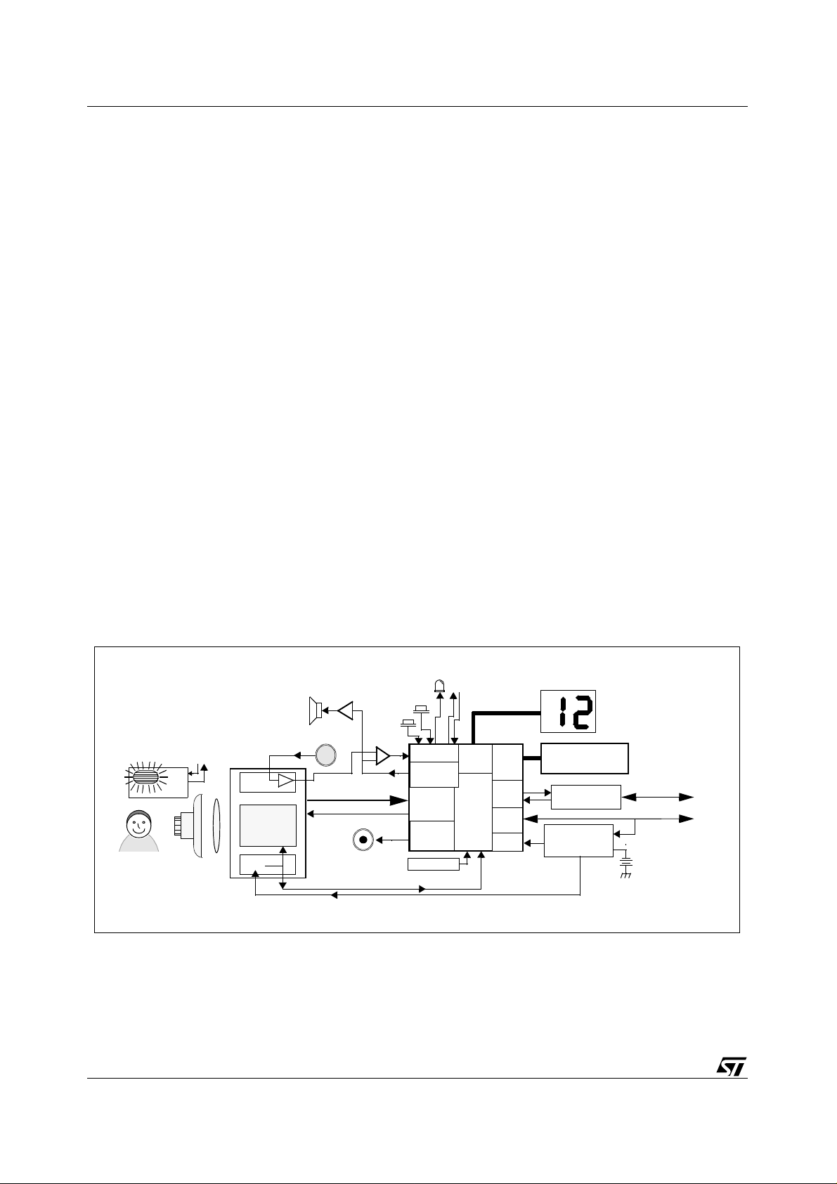
LED
GPIO
Sensor
I/F
PWM
Flashgun
Enable/Trigger
LCD
memory
Driver
STV0680B
I/F
RS232
I/F
USB
I/F
Detect Low
Battery
2 x 7 seg. LCD
16MBit or 64MBit
SDRAM
Transceiver
Circuit (Discretes)
Power
Management
Circuit (Discretes)
RS232 interface
to PC
USB interface
to PC
4.5 - 6v Battery e.g.
3-4 x AA, AAA, etc.
OEM Flashgun
Module
Subject
CMOS Sensor
VV6410/6411(CIF)
VV6500 (VGA)
Enable/Trigger
Lens +
IR Filter
Audio
Pre-Amp
Image Array
VReg
Audio
Speaker
Microphone
Amplifier
Sensor data
Sensor clock
Piezo
Buzzer
Push
Buttons:
“Mode”
“Shutter
/Record”
Comparator
Audio DAC
12MHz XTAL
3v3 supply
4-5v (Nominal) supply from Battery or USB
Figure 1 : Typical camera system block diagram
6/63 Version 3.4
Page 7
STV0680B + VV6444/6410/6500 Introduction
1.2 Co-processor choices
Two revisions of the STV0680B are produced by ST. Although there are certain functional
differences between these revisions, both have an identical pinouts and STV0680B-003 retains all
the functionality of STV0680B-001, hence is backwards compatible.
Order number STV0680B-001 STV680B-003
Silicon revision
Firmware revision
Sensor supported
SDRAM supported
USB
RS232
Video for Windows support
Flash-gun support
Audio record + playback
Custom sounds
Table 1 : Differences between STV0680B-001 and STV0680B-003
1.3 Sensor choices
The following sensors are supported:
STV0680B STV0680B
v1.00 v3.00
VV6444
VV6410
VV6500
16Mbit
or 64Mbit
Yes Yes
Yes Yes
Yes Yes
No Yes
No Yes
No Yes
VV6444
VV6410
VV6411
VV6500
16Mbit
or 64Mbit
Sensor Resolution Sensor supply voltage
VV6444
VV6410/6411
VV6500 VGA (640 x 480)
Table 2 : Sensor choices with STV0680B
1.4 Key system features
The key features of a typical camera based on the STV0680B chipset are as follows:
1.4.1 Image features (STV0680B-001)
● Support for 5V or 3.3V CIF resolution sensor (VV6444 or VV6410/6411) - 352 x 288 pixels
● Support for 3.3V VGA resolution sensor (VV6500) - 640 x 480 pixels
● 80 picture storage capacity possible for CIF, with 64MB memory
● 26 picture storage capacity for VGA, with 64MBit memory
CIF (352 x 288)
5v
3.3v
Version 3.4 7/63
Page 8

Introduction STV0680B + VV6444/6410/6500
● A greater number of images can be stored when ‘Low’ resolution mode is enabled (e.g. 80
QCIF images with 16Mbit memory, 107 QVGA images with 64Mbit memory). See
● Automatic anti-flicker exposure and gain control
Table 3
.
1.4.2 Image features (STV0680B-003)
● All image features for STV0680B-001 are supported.
● Support for flashgun.
1.4.3 User features on camera (STV0680B-001)
● Self-timer mode allows a picture to be captured after several seconds.
● Twin 7 segment LCD panel supported - showing number of pictures left, and modes.
● Picture counter helps the user to know how much memory is left.
● Un-tethered ‘Continuous’ mo de all ow s captur e of i mage sequen ces for storage i n mem ory and
subsequent download to PC.
● Piezo buzzer indicates a number of useful events to the user, e.g. whether enough light is
present for picture capture, etc.
● Indicator LED.
● “Clear all” function clears camera.
● “Low Resolution” mode incre ases number of images wh ich can be captur ed by reducing image
resolution.
1.4.4 User features on camera (STV0680B-003)
● All user features of STV0680B-001 are supported.
● Audio Record function (if audio record hardware detected) allows sounds to be recorded.
● Audio Playback function (if audio playback hardware fitted) allows sounds which have been
recorded to be played back.
● “Delete last” function allows user to delete audio memos, pictures or continuous clips, deletion
must be carried out “most reset first”.
● Camera can be configured by the user to play custom sounds at certain functions, using a PC
application.
● “Go to sleep” function, whereby the camera can be put into standby mode while untethered.
1.4.5 User features on PC software (STV0680B-001)
PC software allows a number of features, including fast download of thumbnail images for picture
selection, and automatic detection and correction of sensor defects. The driver compatibility
includes:
● TWAIN driver to suit all TWAIN compatible imaging applications
● Video for Windows PC driver for tethered video mode (through USB), available at all
resolutions, with fastest framerates at QCIF resolution
● AVI video file creation from image sequences captured in ‘continuous’ mode
● Quicktime Video driver and Adobe Photoshop stills plug-in for Mac
Custom OEM PC software can be developed by using t he SDK (for SDK a vailabilit y, contact ST), to
upload thumbnails/still images or ‘continuous’ images, e.g. for AVI file creation.
8/63 Version 3.4
Page 9

STV0680B + VV6444/6410/6500 Introduction
1.4.6 User features on PC software (STV0680B-003)
All PC software written for a STV0680B-001 camera will function with a STV0680B-003 camera
which is only used to take still images/video.
The SDK (version 2.90 or later) allows for:
● the OEM to write a custom application for uploading sound memos, based on the example
LCDC demo software.
● the OEM to write a custom application for downloading custom sounds to the camera, based
on the example CustomSound software.
1.4.7 Power management features and USB compliance
● Retention of pictures, recorded sounds, and downloaded custom sounds with extremely low
power operation, which appears to the user as if the camera is “switched off”.
● Auto power-off after 30sec with no user activity
● Operates from 4.5-6V battery, although system voltage is 5V or 3.3V, dependant on sensor.
● Low battery detection
● Dependant on hardware configura t io n, swit ch-over to USB power supply is supported, to allow
the device to operate with low batteries or without batteries, when connected to USB.
● Full USB compliance requirements are listed in the USB specification, however, in a camera
designed using this chipset, the following must at least be included: (a) an SDRAM with
sufficiently low self-refresh current, (b) USB inrush protection circuitry, and (c) (in the case of
VV6444 only) a switched 5V sensor supply is used, to maintain sufficient supply voltage to the
5V sensor. See
Section 4
for further details.
1.4.8 General features
● High speed picture/sounds upload to PC/Mac over USB
● ST Colour processing algorithms included under license (as part of drivers/SDK)
● USB or RS232 serial interface options, and VfW / TWAIN driver support.
Version 3.4 9/63
Page 10
Detailed features STV0680B + VV6444/6410/6500
2 Detailed features
2.1 Sensor type and image formats
The sensor type is auto-detected by STV0680B, which ensures that the correct sensor timing is
enabled, and the correct image resolutions are enabled, as shown in
For stills photography, ‘High’ or ‘Low’ resolution mode can be sele cted, to give CIF or QCIF pictures
from a CIF sensor, and VGA or QVGA from a VGA sensor (see
for storage of more images. Images captured in both ‘High’ and ‘Low’ resolution can be stored in
camera memory at the same time. Therefore there is no need for images stored in memory to be
cleared before changing image resolution.
Where USB is connected, the host PC software (through a Video for Windows driver) can activate
tethered video mode, regardless of the user inputs to the camera buttons. In this case, the image
resolution is controlled by the PC driver.
Note: When tethered VfW video (PC) or Quicktime driver (Mac) is activated, all images or recorded
sounds or video clips will be deleted from the camera SDRAM. A software solution is available
(“Camera control”, as part of the SDK for PC, and “Plug’n Save” for Mac) which can monitor
whether a camera is connected and will warn the user if activating the VfW driver will cause SDRAM
contents to be deleted.
Table 3
Table 3
.
). Reduced resolution allows
Sensor
VV6444 CIF 352 x 288
VV6410/
6411
VV6500 VGA 640 x 480
Sensor
Image Size
CIF 352 x 288
Max. no. of
images
Resolution
mode
High CIF 352 x 288 20 80 15 frames/sec.
Low
High CIF 352 x 288 20 80 15 frames/sec.
Low
High VGA 640 x 480 (6) 26 2 frames/sec.
Low
Table 3 : Image modes supported (STV0680B-001)
Final Image Size
QCIF 176 x 144
(Subsampled)
QCIF 176 x 144
(Subsampled)
QVGA 320 x 240
(Subsampled)
stored in
16MBit
memory
(
Note 2
80
80
(26)
)
Max. no. of
images
stored in
64MBit
memory
(
Note 2
)
322
Note 3
(see
322
(see
Note 3
107
Note 3
(see
Approximate
VfW framerate
25 frames/sec.
)
22.5 frames/sec.
)
12 frames/sec.
)
Note: 1 VfW framerate is dependent on PC performance and USB bus loading
2 On a camera using STV0680B-003, the number of images w hich can be stor ed i s reduced if Aud io
sounds have been recorded on the camera or if custom sounds have been downloaded from the
PC to the camera. The reduction of capacity depends on the length of audio clip, but a rough guide
is that if 1 CIF image uses the same amount of SDRAM as 10sec of audio, and one VGA image
uses the same amount of SDRAM as 30 sec. of audio.
(
Note 1
)
10/63 Version 3.4
Page 11

STV0680B + VV6444/6410/6500 Detailed features
3 A CIF camera with STV0680B-001 and 6 4Mbi t SD RAM can store up to 320 i mag es by using QC IF
mode. Where >99 images are still available, the LCD display will remain at 99. Where (no. of
images available) <99, the LCD display will show the number of images available, as is the case
with all other modes.
2.1.1 VV6444
VV6444 is a CIF resolution, 5V CMOS imaging sensor and has been superseded by VV6410/6411.
2.1.2 VV6410
VV6410 is a CIF resolution, 3.3V CMOS imaging sensor . A brief specification is shown in
A dual design to support VV6444 and VV6410/6411 is not possible, since VV6410/6411 is a 3v3
sensor. A single footprint for VV6410/6411 and VV6500 is not possible since the package types
differ, however, the same support circuit is used.
For IR filter design, the best choice filter follows the GS0034 dielectric stack filter specification,
which is available from ST. An alternative, al though not optimal filter, would be Schott S8612 doped
glass, also sold as CM500.
2.1.3 VV6411
VV641 1 is a CIF re solution, 3.3V CMOS imag ing sensor. A brief specification is shown in
The functionality, pixel size, resolution and support circuit are identical to VV6410, however, the
colour filter material is slightly different, and the package type and pinout may differ to VV6410.
Contact ST for further details.
A single footprint to support VV641 1 a nd VV6500 is not possible because of the package dif ference.
A single footprint to support VV641 0 and VV6411 may be possible, dependant on the final package
for VV641 1.
2.1.4 VV6500
VV6500 is a VGA resolution, 3.3V CMOS imaging sensor. A brief specification is shown in
Chapter 6
A dual design to support VV6444 and VV6500 is not possible, since VV6500 is a 3v3 sensor. A
single footprint for VV6410/6411 and VV6500 is not possible since the package types differ,
however, the same support circuit is used. See
Chapter 6
Chapter 6
Chapter 6
.
.
.
For IR filter design, the best choice filter follows the GS0034 dielectric stack filter specification,
which is available from ST. An alternative, al though not optimal filter, would be Schott S8612 doped
glass, also sold as CM500.
2.1.5 SDRAM
This is covered in more details in
2.2 User interface
The user interface supported by STV0680B comprises of user controls, buzzer sounds or
customised audio sounds and visual displays.
2.2.1 Push buttons
The following are the functions which are suppor ted by the chipse t. These functio ns are achievabl e
with no more than 2 push buttons.
Chapter 4
.
Version 3.4 11/63
Page 12

Detailed features STV0680B + VV6444/6410/6500
1 Mode button (Wake-up/Switch between modes): This button allows the user (1.1) to wake the
camera up from standby mode when the camera is to be used for taking pictures, or (1.2) to
switch between modes of operation shown in
2 Shutter button (Shutter/confir m acti on)
an action, as shown in
Chapter 3
: This button allows the user to take a picture or co nfirm
Chapter 3
.
The modes of operation are described in
It may also be desirable to include an on-off slider switch. This has advantages and disadvanta ges,
and its exact function is discussed further in the reference design available from ST.
Where a flashgun module is included in the camera, it will be necessary to include a flash on/flash
off push button or slider switch, dependant on the exact flashgun module design. possible
implementations are discussed in a separate application note AN1312 regarding flashgun
implementation, available from ST.
Chapter 3
.
2.2.2 LED indicator
An LED display camera status, i.e. to show that the camera is not in Standby/PC suspend mode.
2.2.3 Picture counter using 2 x 7 segment display
STV0680B stores a picture counter value, which shows how many images can still be captured.
STV0680B supports a 2x7 segment LCD panel. In ‘Snap shot’ mode and contin uous capture m ode,
this LCD panel displays the number of pictures still available, which is useful to identify when the
user is approaching the maximum number of images which can be stored (see
possible to clear the images stored in memory, in order to continue taking pictures. In other modes,
this LCD panel shows displays a 2-character code, which helps the user to navigate around the
modes.
Note: A CIF camera with STV0680B and 64Mbit SDRAM can store up to 320 images by using QCIF
mode. Where >99 images are still available, the LCD display will remain at 99. Where (no. of
images available) <99, the LCD display will show the number of images available, as is the case
with all other modes.
Table 3
). It is
For suitable numeric LCD panel types, see
Section 4.8
2.2.4 Piezo buzzer
An on-chip Pulse Width Modulator (PWM) on STV0680B is used to generate buzzer sounds to
signal certain events. The following are typical of the type of events which are indicated by the
buzzer, and each has its own distinctive sound:
1 Camera has been ‘Woken up’ from standby mode (either by the user pressing a button, by re-
connecting the power source, or by connecting a USB/RS232 connection).
2 Camera has been ‘gone to sleep’ i.e. moved into standby mode. Pictures are retained in
memory.
3 Picture has been successfully taken after the user presses the capture button.
4 Picture has NOT been taken after the user presses the capture button. This indicates to the
user that there is insufficient light, or that the exposure control was not ready due to a rapid
change of lighting in the scene.
5 Picture has NOT been taken after the user presses the capture button, due to picture counter
having reached the maximum num ber of i ma ges. The u ser ha s the cha nce to zer o th e counte r
if desired.
6 End of continuous capture in un-tethered ‘Continuous’ mode, due to memory full.
7 Self-timer activated and counting down.
12/63 Version 3.4
.
Page 13
STV0680B + VV6444/6410/6500 Detailed features
2.2.5 Custom sounds
A camera which includes STV0680B-003 and Audio playback hardware can have a set of custom
sounds downloaded from a PC application. A different sound can be associated with each of the
following functions:
Power On Sound delete
Power Off Continuous clip delete
Good picture Clear memo ry
Bad picture
(Normally due to insufficient light)
Memory full Low power
Self timer #1 Flashgun ON
Self timer #2 Flashgun OFF
Low resolution Flashgun Trigger
High resolution Frequency 50kHz
Picture delete Frequency 60kHz
Table 4 : List of custom sound functions
Confirm action
Note: 1 Where a given function has a sound associated with it stored in SDRAM, the piezo buzzer does not
give any beeps for that function. Not all functions need to have custom sounds associated with
them, this is the choice of the user or OEM.
2 A demonstration PC application “CustomSoun ds” is available from ST, however this is not intended
for end-users. Source code is available which allows the EOM to build their own PC application
using the SDK.
2.3 Battery level detect and USB auto-switch
An on-chip battery level detector on STV0680B detects when the battery voltage falls below a
threshold. This threshold is determined by the designer, dependant on the perception of what
remains as ‘acceptable’ image quality as the battery voltage falls. The chosen threshold level is
determined by a resistor value, as sho wn in
display flashes, which indicates tha t the battery is low . Whe re a USB connection ha s been detected,
the camera sources power from USB, if certain additional hardware is fitted.
Chapter 6
Where no USB has been detected, the LCD
Note: It may be a requirement of certain USB compliance tests that such additional hardware is included
in the camera design, in order to enable th e camera to switch to supply fr om USB and hence r eport
back to the PC while connected to the USB bus without a battery.
2.4 Audio record and playback
2.4.1 Record
A camera which includes STV0680B-003 and a mi croph one, comparator and other peripher y (also
utilizing the sensor pre-amplifier) can be used to record sounds which are stored in the same way
as images. STV0680B-003 will auto-detect the presence of Audio record hardware and include
Version 3.4 13/63
Page 14

Detailed features STV0680B + VV6444/6410/6500
audio record and “delete l ast” functions int o the user i nterface. The a udio sample rate is 11.025kHz,
and the signal is digitised using a successive approximation A-D converter with 8 bits resolution.
The SDRAM stores 1 second of Audio recording per 11k Bytes of memory.
2.4.2 Playback
A camera which includes STV0680B-003 and an amplifier, speaker/headphone socket, and other
periphery, can be used to playback sounds which were either recorded on the camera or
downloaded from the PC.
The quality of Audio playback is largely depe ndant on the type of speaker used, and on the correct
mounting of the speaker in the camera plastics.
2.5 PC interface options and software support
Either USB Interface (full speed 12Mbit/sec. max.) or RS232 interface (115.2Kbaud) is supported
by the chipset, with driver software available from ST for both. The interface type is auto-detected
by the chipset. PC software can be one of the following:
1 Simple image upload demonstration software supplied by ST, allowing uploading of stills or
‘continuous’ images. This software should not be supplied as an end-user product.
2 TWAIN driver to suit all TWAIN compatible imaging applications
3 Video for Windows driver for tethered video mode (USB only)
4 Custom end-user software developed by OEM using SDK (for SDK availability, contact ST).
The SDK is supplied by ST as a 32-bit DLL format, running on Windows 98, and accessed
through a documented software interface. This provides the basis for developing a custom
software application for uploading stills and/or video.
2.5.1 USB
Complete images (displayed as either thumbnails or in full resolution), or the entire SDRAM
contents (e.g. for uploading continuously captured image sequences, recorded using ‘Continuous
Capture’ mode) can be downloaded through USB, and USB connection also allows for tethered
video mode to be activated by the USB driver.
Thumbnail image download is extremely fast for the enti re memory cont ents in the camer a. Once a
picture is selected fo r down load, full image download takes approximately 0.15 seconds per ima ge
for a CIF image (0.6 seconds for a VGA image), plus post processing time per image.
For USB interface details, see
Section 4.4
.
Note: Actual USB download and post processing time also depends on PC performance and USB bus
loading
2.5.2 RS232
Thumbnails of images, complete stored images, or the entire SDR AM contents can be downloaded
through RS232, but tethered video is not supported.
Once a picture is selected for download, full image download takes approximately 10 seconds per
image for a CIF image ( aro und 3 0 second s for a VGA i mage), plus post processing time pe r i m age
(of the order of 1 second approximately).
For RS232 interface details, see
Note: Actual post processing time after RS232 download also depends on PC performance
Section 4.5
.
14/63 Version 3.4
Page 15
STV0680B + VV6444/6410/6500 Detailed features
2.6 Anti-flicker exposure and gain control
2.6.1 General
The chipset operates automatic exposure and gain control for either 50Hz or 60Hz mains-driven
indoor lighting, using the same 12MHz crystal. This improves picture quality by selecting a set of
exposure values which minimise ‘f li cker’ effects. Detection o f the mai ns fr equen cy is dep endan t on
the status of the GPIO3 pin, which can be achieved by population of a PCB link at a late stage in
production, once the country of destination is known, without the need to change the crystal
frequency.
The auto exposure and gain algorithm is always enabled during Snapshot’/self-timer/continuous
mode. When the shutter button is pressed in ‘ Snapshot’ mode , the chipset captu res an image if the
exposure and gain value has reached a suitable val ue for the current scene. If the li ght detected has
suddenly changed, the camera may emit an audible tone to indicate that more time is required to
reach the correct exposure target. In ‘Snapshot’ mode the chipset only captures the image data if
sufficient light is present in the image. In continuous capture mode, the chipset captures images
regardless of whether enough light is present.
The exposure control algorithm in STV0680B chooses exposure values which minimise “flicker”
effects from occurring under fluorescent lighting. STV0680B can only prevent flicker in lighting
powered by 50Hz or 60Hz electricity supply, but automatic detection of the flicker frequency is not
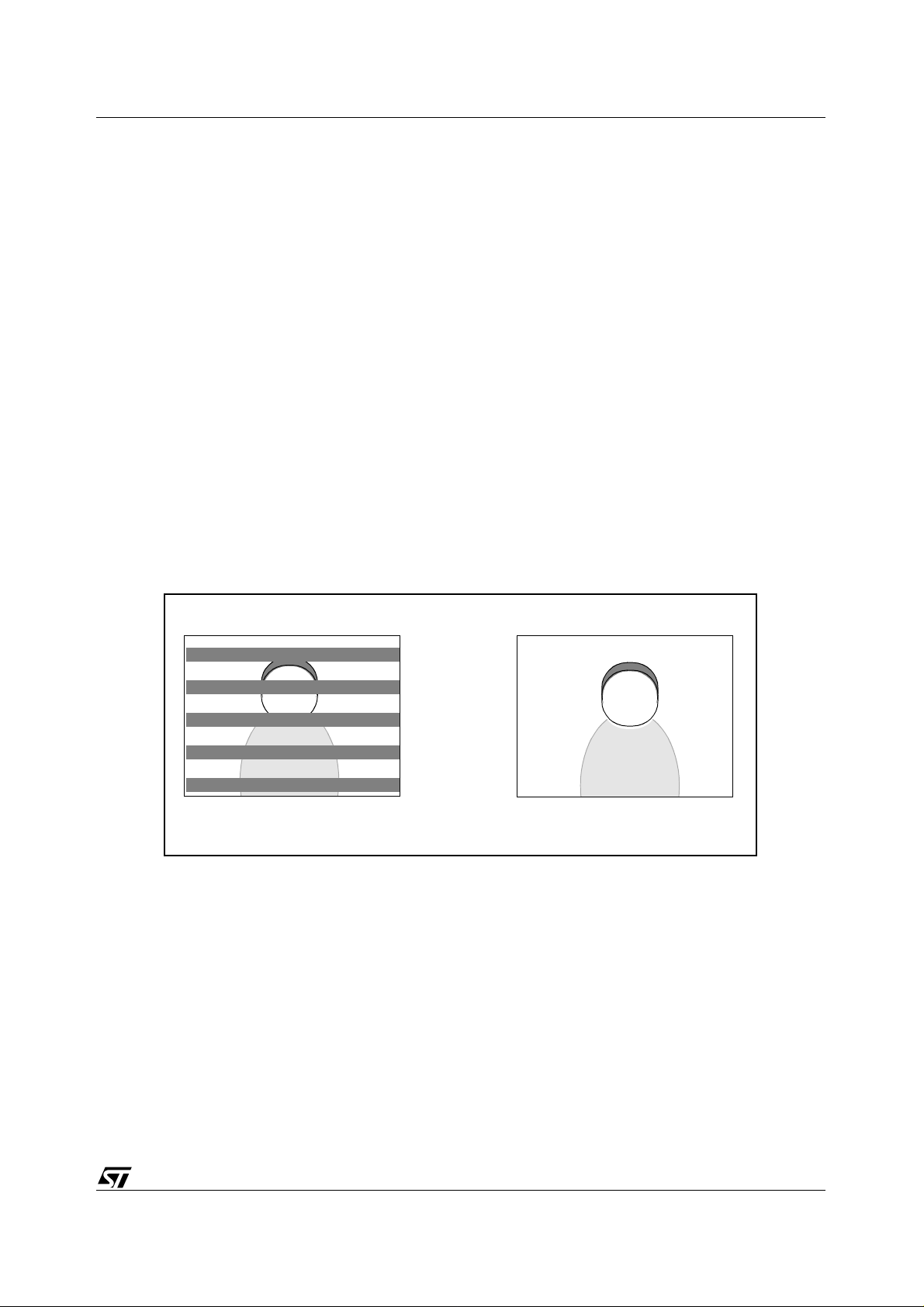
possible. Hence choosing the correct anti-fli cker setting is importan t, in order to prevent da rk stripes
form appearing across the image, and this selection must be done in hardware.
Flicker setting not correct Flicker setting correct
2.6.2 Flashgun exposure
Where STV0680B-003 and a flashgun module are in cluded in the camera, and the flashgun enable
signal is HIGH, the exposure mode will operate in a different manner. The CMOS sensor
progressive scan readout requires that the sensor is set to maximum exposure so that all lines are
being exposed at a certain point in time.
The “window” within which the flashgun needs to fire in order to correctly expose all sensor lines is
of the order of a few 100µsec (contact ST for more precise details), therefore the flashgun module
design should have reached maximum light output within this period after the falling edge of the
flash trigger output from STV0680B-003.
Figure 2 : Illustration of flicker problem
Possible flashgun implementations, regarding hardware interface, charge sensing, and flash
energy required are discussed in a separate application note AN1312 regarding flashgun
implementation, available from ST.
Version 3.4 15/63
Page 16
Camera modes of operation STV0680B + VV6444/6410/6500
3 Camera modes of operation
This section refers to the two switches as discussed in section
● “Mode”: connects GPIO0 pin of STV0680B to GND when pressed
● “Shutter”: connects GPIO1 pin of STV0680B to GND when pressed
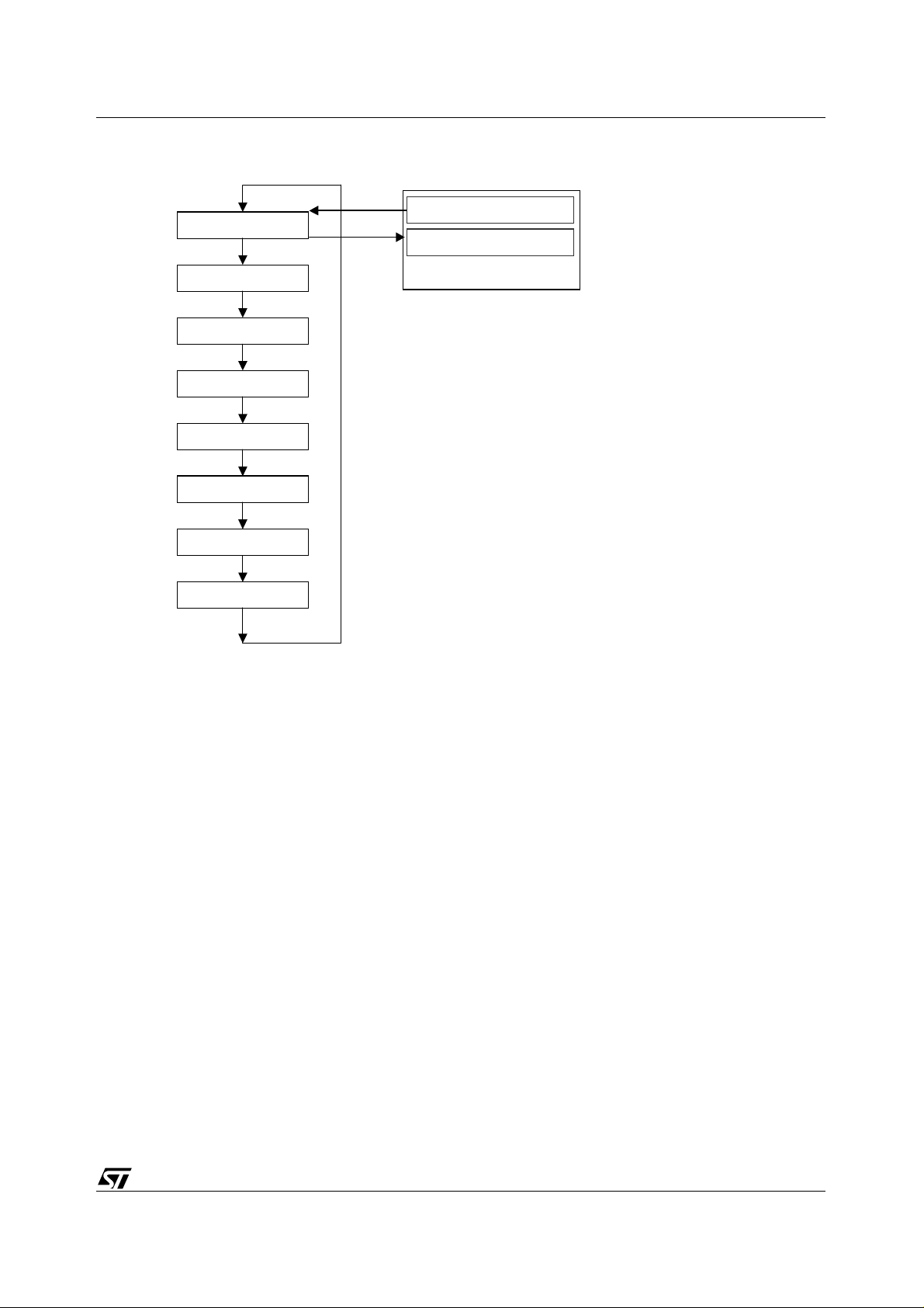
Pressing the mode switch repeatedly cycles through a series of modes as displayed on the LCD.
When a given mode is displayed it may be selected by pressing the shutter button. If an option is not
selected within 5 seconds the display will revert to showing the number of available pictures.
3.1 Modes available (STV0680B-001)
Normal: 20 / 80
Continuous Capture: Ct
Self-Timer: St
Clear All: CL
Re solution: Hr / Lr
Press Mode button
After 30sec of inactivity
Standby mode (u ntethered)
Section 2.2.1
Figure 3 : STV0680B-001modes (CIF camera with 16Mbit SDRAM assumed)
Note that the number of images displayed depends on the sensor and SDRAM type - see
16/63 Version 3.4
Table 3
.
Page 17
STV0680B + VV6444/6410/6500 Camera modes of operation
3.2 Modes available (STV0680B-003)
Normal: 20 / 80
Audio Record: Ar
Audio Playback: AP
De lete Last: dA / dP / dC
Continuous Capture: Ct
Self-Timer: St
Clear All: CL
Re solution: Hr / Lr
Press Mode button
After 30sec of inactivity
Standby mode (u ntethered)
Notes:
1. Audio Record only available if audio hardware is fitted
2. Audio Playback only available once an audio clip has been recorded
3. Delete Last displays (only available if audio hardware fitted)
dA - if the last object is an audio clip
dP - if the last object is a picture
dC - if the last object is a continuous capture clip
The mode is inhibited if the camera is empty.
4. Continuous Capture mode is inhibited when the flashgun is enabled
(SW 6 down)
Figure 4 : STV0680B-003modes (CIF camera with 16Mbit SDRAM assumed)
3.3 Description of modes
Note that certain modes are only available using STV0680B-003, and with appropriate hardware
fitted on the camera.
3.3.1 Standby mode (untethered) and Wake-up
On power-up, or wake-up from untethered standby mode, (i.e. by pressing the Mode button), the
camera will beep twice. The LCD will briefly indicate the camera resolution either ‘Hr.’ for high
resolution (80 CIF or 26 VGA images - usi ng 64Mbit memo ry) or ‘Lr’ for low resolution (32 2 QCIF or
107 VGA images - using 64Mbit memory) and then display the number of pictures which may be
taken. Please note that in Low Resolution Mode, although t here can be up to 322 images availab le,
the LCD counter will only go up to 9 9, it will contin ue reporting 99 un til there are less than 99 images
left.
The camera will go back to standby mode either after 30 seconds of inactivity, LED1 will turn off and
the LCD will go blank. This can al so be done (STV 0680B-003 only) by pressing t he mode switch f or
more than 2 seconds.
3.3.2 Normal mode
Pressing the shutter button will take a pi cture . T he camer a wi ll beep. A h igh pi tched beep indi cates
that the picture was taken successfully and the counter will decrement (if there are less than 99
images left to take). A low beep indicates insufficient light to take a picture. A series of beeps
indicates that the camera is full.
Version 3.4 17/63
Page 18

Camera modes of operation STV0680B + VV6444/6410/6500
Stored pictures may be uploaded t o a PC at any time, whether or not the ca mera is full. Plugging the
USB connector into the camera will cause it to r eset and issue a double b eep but all stored p ictures
will remain. When the USB connector is unplugged the ca mera will go to sleep. When connected to
the PC the camera may still be used in the normal way.
Note
: With the flashgun enabled (STV0680B-003 only) the camera will always take a picture,
whether or not there is sufficient light.
3.3.3 Audio record - Ar
This mode is available on STV0680B-003 only, with audio record hardware fitted.
Pressing the shutter button with in 5 secon ds w ill cause the camera to start recordi ng for as l ong as
the shutter button is pressed down. If the shutter butto n is not pressed withi n 5 seconds the camera
will revert to normal picture taking mode. Whilst recording, the LCD display flashes ‘Ar’. If the
recording stops because the memory is full, the ‘memory full’ audio tone is so unded and the displa y
will stop flashing and display ‘00’. The audio data is digitised and stored in SDRAM.
3.3.4 Audio Playback - AP
This mode is available on STV0680B-003 only, with audio playback hardware fitted.
Pressing the shutter button within 5 seconds will cause the camera to play back the most recent
audio recording. If the shutter button is not pressed within 5 seconds the camera will revert to
normal picture taking mode. Whilst playing, the LCD display flashes ‘AP’.
Once in Audio Playback mode, repeated presses of the shutter button will step the camera through
each of the audio recordings in the camera (most recent first). Keeping the shutter button pressed
down will also cycle through the audio recordings. Pressing the mode button during playback will
stop the audio clip.
Note
: Minimum audio recording length is set to 0.5 seconds.
3.3.5 Delete last object - dA/dP/dC
This mode is available on STV0680B-003 only, with audio record hardware fitted.
If the last object captured was an audio recording 'dA' (delete audio) will be displayed, if the last
object was an image, then 'dP' (delete picture) will be displayed, or, if the last object was part of a
continuous capture sequence, then 'dC' (delete continuous) will be displayed. If the camera is
empty , the mode will be suppressed. The mode works in the same way as ‘CL’ (Clear All), i.e. once
the mode is selected, pressing the shutter button once will cause the camera to b eep and ‘dA’, ‘dP’
or ‘dC’ to start flashing. Pressing the shutter butto n again within 5 seconds will delete the l ast audio
clip, picture or continuous capture sequence.
18/63 Version 3.4
Page 19

STV0680B + VV6444/6410/6500 Camera modes of operation
3.3.6 Continuous mode - Ct
Pressing the shutter button within 5 seconds will cause the camera to start taking pictures for as
long as the shutter button is pressed down (and the camera is not full). If the shutter button is not
pressed within 5 seconds the camera will revert to normal picture taking mode.
Note: 1 During continuous mode the camera wil l allow picture s to be ta ken regardl ess of the ava ilable light,
which could result in insufficient exposure.
2 In continuous mode, only every alternate field is grabb ed hence capture rate is halved. E.g. 12.5 fps
CIF and 7.5fps VGA
3 On STV0680B-003, Continuous Mode is suppressed w hen the Fl ashGun ena ble signal ( GPI O2) is
high.
3.3.7 Self timer - St
Pressing the shutter button will now start a 10-second self-timer . The camera will issue a short beep
every second and then a longer beep. A further beep will then indicate that the picture has been
taken (high beep - picture successful, low beep - insufficient light, picture not taken). The self-timer
mode can not be selected when the camera is full. The self-timer countdown cannot be stopped
once it has started.
3.3.8 Clearing the camera memory - CL
Pressing the shutter button once will cause the camera to beep and the ‘CL’ to start flashing.
Pressing the shutter button again within 5 seconds will clear all the images/audio clips in the
camera and reset the counter.
3.3.9 Changing picture resolution - Hr/Lr
The resolution option is displayed, either Hr. to change to high-resolution mode (if currently in lowresolution mode) or Lr to change to low-resolution (if currently in high-resolution mode). Press the
shutter button within 5 seconds of selecting the resolution option, the camera will beep and the
display will reset indicating the number of pictures available in the new mode. The picture resolut ion
can be changed at any time, i.e. the camera can store both high and low resolution images.
Version 3.4 19/63
Page 20

STV0680B hardware interfaces STV0680B + VV6444/6410/6500
4 STV0680B hardware interfaces
4.1 STV0680B pinout
The STV0680B pinout has been carefully developed to minimise the physical size of the support
printed circuit board by facilitating placement of and electrical routing to peripheral support
components such as the SDRAM. The complete pinout and listing is shown in
4.2 Sensor interface
STV0680B uses a standard ST digital interface from the sensor, and the sensor clock input is
provided by an output from STV0680B. Designing a camera using this chipset should design as
close as possible to the reference design (
a functional ‘black box’, and no further details regarding the STV0680B-sensor interface are
required.
4.3 Memory inte rface
Chapter 6
), in which case the chipset can be regarded as
Chapter 6
STV0680B is designed to interface to an external 16Mbit or 64Mbit SDRAM (see
SDRAM device must have a 16 bit wide data bus and operate from a 3.3V supply. Two sizes of
SDRAM memory are supported by STV0680B, 16MBits (1M x 16 bits wide) or 64MBits (4M x 16
bits wide), the memory size is auto-detected by STV0680B. STV0680B clocks the SDRAM at
6MHz, typically this is we ll below the fi gures offer ed by most manufacturers ’ devices. Devices whic h
are PC66 and/or PC100 compliant are preferred. For interface wiring, see
4.3.1 SDRAM current consumption
For maximum system battery life while no pictures are being taken, and to assist in meeting
requirements for USB compliance, an SDRAM should be chosen with the lowest possible self
refresh current specification. For suggested SDRAM part numbers, see
In addition, the USB suspend mode current specification require s that the camer a will consume no
greater than 300µA when un-tethered. Meeting this specification, which is included in the
requirements for USB compliance, assumes an SDRAM with up to approximately 250µA selfrefresh current, based on a current consumption of approximately 50µA for STV0680B+support
circuit.
4.3.2 SDRAM interface timing requirements
The following timing diagrams should be referred to when selecting SDRAM other than those
recommended in
Chapter 6
Chapter 6
Chapter 6
Table 3
). The
20/63 Version 3.4
Page 21

STV0680B + VV6444/6410/6500 STV0680B hardware interfaces
DCLK
CKE
Command
A0-9,BA
A10
DQM
DQ
t
CK
t
CMS
ACTIVE
t
CMH
t
L
READ
t
H
NOP PRECHARGE NOP
ROW COLUMN
ROW
t
AS
t
t
RCD
t
CMS
AH
t
t
AC
OH
DOUT M
READ Latency
t
RAS
DQ sample DQ sample DQ sample DQ sample
Figure 5 : SDRAM read timing (16Mbit device, burst read)
t
CMH
DOUT M + 1 DOUT M + 2 DOUT M + 3
t
RC
t
RP
DCLK
CKE
Command
A0-9,BA
A10
DQM
DQ
t
CK
t
CMS
ACTIVE
t
CMH
t
L
WRITE
t
H
NOP PRECHARGE NOP
ROW COLUMN
ROW
t
AS
t
t
CMS
AH
t
t
DH
DS
t
DIN M
RCD
DIN M + 1 DIN M + 2 DIN M + 3
t
RAS
Figure 6 : SDRAM write timing (16Mbit device, burst write)
t
CMH
t
RC
t
RP
Version 3.4 21/63
Page 22

STV0680B hardware interfaces STV0680B + VV6444/6410/6500
Symbol Min. Max Units Symbol Min. Max Units
t
CK
t
CH
t
CL
t
AC
t
OH
t
CMS
t
CMH
t
AS
166.45 166.89 ns
½
½
½
0ns
82.88 ns
82.85 ns
82.88 ns
Table 5 : Timing parameters for SDRAM read/write
4.3.3 SDRAM refresh period
The SDRAM refresh period from STV0680B is guaranteed to be no greater than 15.6µS during
‘Snapshot’/self-timer/continuous/tethered video modes of operation (i.e. not standby mode). In
standby mode, the SDRAM is set to self-refresh, therefore no refresh from STV0680B takes place.
4.3.4 SDRAM initialisation period
The SDRAM initialisation period is currently set to 981µS in STV0680B.
t
DS
t
CK
t
CK
t
CK
t
DH
t
RCD
t
RAS
t
RC
t
RP
t
RCD
t
AH
81.01 ns
83.41 ns
1
55
7
2
1
t
t
t
t
t
82.76 ns
CK
CK
CK
CK
CK
4.4 USB interface
STV0680B includes a USB Version 1.1 compliant Universal Serial Bus Interface, including a
transceiver. This allows direct connection from STV0680B to a USB connector with minimal
additional hardware (i.e. a small number of passive discretes) - see
The USB interface interf aces the STV0680B to the USB at full spee d 12MHz data r ate. Some of the
features are:
● Compliant with USB protocol revision 1.1.
● USB protocol handling.
● USB device state handling.
● Clock and data recovery from USB.
● Bit stripping and bit stuffing functions.
● CRC5 checking, CRC16 generation and checking.
● Serial to parallel conversion.
● Single bulk end point.
USB drivers are supplied by ST. For USB timing information, please refer to the USB specification
V1.1.
Chapter 6
22/63 Version 3.4
Page 23

STV0680B + VV6444/6410/6500 STV0680B hardware interfaces
4.5 UART module for RS232 interface
The UART module on STV0680B p rovides a 115200 baud full duplex interface to a n exter nal H ost.
4.5.1 RS232 physical interface
STV0680B does not support direct connection to a serial link. Physical line driver circuitry is
required, e.g. using a standard RS232 transceiver chip, or by using a small number of low cost
discretes (as shown in
no greater than 2m. Unscreened cable can be used, a suitable low cost connector is a 3.5mm audio
jack plugs/sockets.
4.5.2 UART module overview
Receiving data
The UART module in STV0680B receives serial data through the RXD pin. Data reception is
initiated by a 1-to-0 transition on RXD, and the received data is sampled every 8.66µS.
If the RXD input is not 0 when the incoming data is first sampled, the UART module goes back to
look for another 1-to-0 transition . This i s to pr ovi de r ejectio n of fal se star t bi ts. If th e start bit proves
valid, reception of the rest of the frame will proceed.
Transmitting data
Chapter 6
). The schematics shown assume a 3 core cable with a length of
When a transmission is activated by STV0680B, the contents of an internal transmit shift register
are shifted onto the TXD pin, every 8.66µS.
The UART operates at 12MHz, whi ch is not an i nteger multi ple of 115200, so the actual baud rate is
115232 +/- 0.3%, which is well within the requirements of a typical 16x oversampling UART, which
can tolerate a 3.75% error in baud rate.
4.6 Power management and battery type
STV0680B and the SDRAM require a 3.3V sup ply. Where a VV6410/6411 or VV6500 (3.3v) sensor
is used, a single voltage regulator can be used to regu late the supply for all t hree compon ents from
the battery, or the sensor on-board VReg can be used. Where a VV6444 is used, the sensor
requires a 5V supply, hence a DC-DC converter is recommended to provide enough voltage when
the camera is powered from the USB bus. These are explained more fully in the reference design.
4.6.1 Power switching to USB
Included in the USB compliance requirements, is the abil ity of the camera to report to the PC when
connected to the USB bus, whether or not there is a fresh battery in the camera. This means that
power sourcing from USB is required, which also saves on battery life while the camera is used in
USB tethered video mode. In order to allow switching from battery to USB power, some additional
hardware is required (see also
● The USBDETECT input to STV0680B is used to detect that a USB power supply is connected
● If the USB is detected, additional hardware is used to switch off the battery
● An inrush protection circuit can protect the USB bus from current draw in the case of a low
battery/battery not fitted. This may be necessary to comply with the USB specification.
Chapter 6
):
For precise USB compliance requirements, please consult the USB specification version 1.1
4.6.2 Switched sensor supply
Dependant on the hardware implementatio n, the SENSPWR output from STV0680B can be used to
power off completely the sensor during Standby mode (in the case of VV6444) or put the sensor
Version 3.4 23/63
Page 24

STV0680B hardware interfaces STV0680B + VV6444/6410/6500
into Suspend mode (in the case of VV6410/6411/6500). This has a significant improvement on
battery life.
4.6.3 Battery type
This is hardware dependant. The schematics referred to in
1.5V cells.
4.7 Quartz crystal
Regardless of the sensor type or anti-flicker requirements, the sensor + STV0680B chipset
operates from a single 12MHz fundamental quartz crystal. For specification requirements, see
Table 13
. STV0680B includes an on-chip low jitter PLL, for PLL characteristics, see
4.8 Numeric LCD interface
STV0680B supports a 2-digit LCD panel only, for alpha-numeric display.
4.8.1 LCD types
STV0680B connects to a non multiplexed, direct drive LCD with 2 x 7 segments. Many LCD types
are compatible with this interface. The LCD refresh frequency is 34.7Hz.
4.8.2 LCD interface pinout
The convention for segment numbering is as follows: ’0’ connects to segment ’a’, ’1’ connects to
segment ’b’, and so on, where a to g are standard for all 7-segment displays, as well as an LCD
common output, giving fifteen signals in total.
Chapter 6
assume either three or four
Table 12
.
4.9 Switches and LED’s
The GPIO lines on STV0680B have pre-defined functions as follows, see
interface functionality, and
Chapter 6
for precise hardware implementation
4.9.1 MODE push button and SHUTTER push button: GPIO0 and GPIO1
Both push button inputs have internal de-bounce circuits, reduci ng the amount of hardware required
externally. It is recommended that labelling is used on the camera casing to help the user
understand the functioning of the 2-button interface.
4.9.2 Input to select between 50 and 60Hz flicker frequency: GPIO3
This allows for factory setting of the anti-flicker frequency, dependant on the final country of
destination. See also
(see
Chapter 6
).
Section 2.6
. The polarity of this selection is detailed in the reference design
4.9.3 LED indicator output: GPIO5
The LED output has an 8mA current sinking capability.
4.9.4 Other pins: GPIO2, 4, 6, 7
With STV0680B-001, these pins are un-used and should be tied to GND.
Section 2.2
for user
24/63 Version 3.4
Page 25

STV0680B + VV6444/6410/6500 STV0680B hardware interfaces
With STV0680B-003, these pins are used, as detailed in
GPIO 2 4 6 7
Audio Reco rd No Yes No No
Audio
Playback
Flashgun Yes No No Yes
No No Yes No
Table 6 : Other GPIO usage with STV0680-003
Table 6
Their specific functions are detailed in the reference design and in the following documents
available from ST:
● Audio: Application note AN1310
● Flashgun: Application note AN1312
4.9.5 Audio record hardware interface (STV0680B-003 only)
The firmware implements a successive approximation A/D conversion by outputting successive
analogue levels through the DAC output, which are compared with the actual signal level (output
from the sensor microphone preamplifi er), and the resul tant high or low signal from the compar ator
is read at GPIO4. The sampling frequency is 1 1kHz, and the successive approximation is done at 8
bits resolution per sample. It i s not possible to speed u p the sampling frequen cy due to the limitation
of STV0680B firmware speed.
An actual hardware implementation is given in the audio application note AN1310.
.
4.9.6 Audio playback hardware interface (STV0680B-003 only)
The firmware outputs the desired signal level through the DAC output, which is amplified to the
speaker or headphone socket. GPIO6 is used to switch off the amplifier during periods of audio
recording, to prevent the successive approximation waveform from being heard during periods of
recording, and to reduce the power consumption and unwanted crackle through the speaker.
An actual hardware implementation is given in the audio application note AN1310.
4.10 Flashgun hardware interface (STV0680B-003 only)
STV0680B-003 will revert to flashgun e xposure when it dete cts GPIO2 is high . Ideally t he hardwar e
should combine the two factors of (a) user intentio n (e.g. user switches on flashgun ) and (b) charge
sensing (i.e. flash is charged up and ready to fire).
These two factors (a) and (b) are independent, since there may be a delay of several seconds
between switching on the flashgun charge r , and the flashg un being able to fi re. To revert to flashgun
exposure before the flashgun is completely charged up would cause very bad pictures to be taken
in low light conditions because ther e is no “low lig ht” threshol d when flashgun exposure is enabled,
since the camera expects a flash to fire. A suggested flashgun hardware interface is given in the
flashgun application note AN1312.
When flashgun exposure is enabled and the shutter button is pressed, a picture will be taken and
the flash trigger pin GPIO7 will be pulsed low at the correct point in time so that all lines of the
CMOS imager are exposed.
4.11 IR filter
An Infra-Red Blocking Filter is re qui red to achi eve corre ct colour r esponse. The exact specifi cati on
for the IR filter characteristics are given in the reference design manual.
Version 3.4 25/63
Page 26

Software support STV0680B + VV6444/6410/6500
5 Software support
5.1 General features
The chipset is a dual-mode camera, i.e. stills and video, and is supported by a range of
demonstration software, standard drivers, and software development options.
Driver software is available to support both USB and RS232 interface including standard TWAIN
and video for Windows drivers (VfW through USB only) for Wi n98/Win2k/Wi nME. Quicktime drivers
and a Photoshop stills plug in for MacOS 8.6/9.0/9.1 are also supported.
Example software applications (PC only) are provided to create .AVI video files from untethered
continuous capture of images (AVICreator), to upload still images and recorded sounds
(LCDCdemo) and to download .W A V files from the PC to the camera (CustomSound). In each case,
PC source code is provided to assist in OEM software development using the SDK.
ST colour processing and defect detection/correction software runs on the host and is supplied
under licence agreement, as part of all host software/drivers/SDK.
5.1.1
Still image
upload
This is available throug h demonstrat ion softwa re, OEM cust om software, or using standard T W AIN
applications. Features include:
● Fast upload through USB, or upload through RS232.
● Colour display of image thumbnails for picture selection.
● Download of full image once selected by user software.
● Automatic detection and correction of sensor defects
● Colour processing of full image, using the ST colour process
The above features also apply to “AVI Creator” or any OEM custom softwar e fo r AVI video creation
from pictures taken while un-tethered, since this is essentially a “stills” function.
5.1.2
Streaming video
(only while tethered to USB)
This is available through demonstration software, or using standard VfW applications. Features
include:
● Streaming video through standard VfW driver
● Automatic detection and correction of sensor defects
● Colour processing of full image, using the ST colour process
5.2 Software installation
The following software support is only available to OEMs. Access to the latest installation files is
possible through a password-protected web page, contact ST for details. The install file gives the
option to install:
● Drivers (always check web site for latest driver version).
● EVK software, i.e. LCDCdemo.exe and AVIcreator.exe, G2Video.exe, and CTItest2.exe
● SDK installation: source code for sample applications, and documentation
26/63 Version 3.4
Page 27

STV0680B + VV6444/6410/6500 Software support
5.2.1 Driver support available
Interface type:
PC Operating system:
Mac OS
STV0680B-001
STV0680B-003
RS232 USB
Win9x, WinNT4, Win2k, Windows
Millennium
N/A 8.6, 9.0, 9.1
TWAIN TWAIN, VfW
Table 7 : Driver choices
Win98 and Win2k only, Windows
millenium
5.2.2 EVK software
Note: The following is also supplied with evaluation kit s/demonstration u nits, but all the follow ing software
is only for demonstratio n pu rposes and sho ul d N OT b e supp lied as an end-user product. However,
application-level source code (i.e. not driver/colour processing source) for LCDCdemo.exe, AVI
creator , and CTItest.exe is avai lable as pa rt of the SDK, which all ows similar appli cations to be buil t
by the software developer:
1 Simple demonstration software LCDCdemo.exe for uploading thumbnails and images.
2 AVIcreator.exe software for uploading continuous images for creating ‘movie’ clips.
3 G2Video.exe is a VfW application which shows streaming video while tethered to USB and
allows creation of.AVI video clips.
4 CTItest.exe is only for debugging purposes, for software developers using the SDK
5.2.3 Software Development Kit (SDK) and source code
A software development kit allows the OEM to develop a custom application which calls the same
range of drivers as listed in
download, thumbnail display, and colour processing using the ST colour process. Inclusion of
source code for the applications listed in
as the basis for their own application.
The SDK is supplied by ST as a 32-bit DLL format, running on Windows 98/Wi n2K
through a documented software interface. Development requires Microsoft Visual Studio Ver. 6 or
later. This provides the basis for developing a custom software application for stills.
Note: Source code for PC Drivers, Defect Correction, and Colour Processing algorithms ar e not available.
Section 5.2.1
, hence allowing the OEM application to perform picture
Section 5.2.2
allows the software developer to use these
TM
, and accessed
Version 3.4 27/63
Page 28

Detailed chipset specifications STV0680B + VV6444/6410/6500
6 Detailed chipset specifications
6.1 Typical camera specifications
The following data assumes that the camera has been built accor ding to referen ce design shown in
Chapter 6
Supply Voltage
Operating Te mpe ra ture range
Max. RS232 cable length supported
CIF output
QCIF output
VGA output (using VV6500)
QVGA output (using VV6500)
SDRAM storage and image upload format
PC driver output format
Table 8 : Typical camera specifications
4.1-6V (when powered from battery or USB)
0oC - 40oC
2m
352 x 288 pixels
176 x 144 pixels
640 x 480 pixels
320 x 240 pixels
Raw Bayer
Colour RGB bi tmap
Note: 1 Dual USB or battery power supply is only possible when the required power switching
hardware is included, as shown in Chapter 6
2 Figures are approximate and depend on actual components sources.
Sensor Min. Max
VV6444 8.18µS39mS
VV6410/6411 8.67µS44mS
VV6500 7.94µS66mS
Table 9 : Approximate shutter speeds
28/63 Version 3.4
Page 29

STV0680B + VV6444/6410/6500 Detailed chipset specifications
6.2 STV0680B companion processor
Parameter Min. Typ. Max. Units
Supply voltage 3.0 3.3 3.6 V
Current consumption (normal operation) 20 - mA
Stand-by current consumption
(untethere d standby or tethered PC suspend m o de)
--5µA
Operating temperature range 0 - 70 °C
Package 100QFP
Exposure control 1 000 000 : 1
Storage Temperature (Approx i ma te ) 50 to 150
o
C
Table 10 : STV0680B specifications
Parameter Description Min. Typ Max Units Notes
VDD Power Supply 3.0 3.3 3.6 V
V
V
V
V
V
V
V
V
ILU
IHU
IHUZ
DI
CM
OLU
OHU
CRS
USB differential pad D+/D- input low 0.8 V
USB different i al pad D+/D- input high (driven) 2.0 V
USB differential pad D+/D- input high (floating) 2.7 3.6 V
USB differential pad D+/D- input sensitivity 0.2 V 1
USB differential pad D+/D- common mode voltage 0.8 2.5 V 2
USB differential pad D+/D- output low voltage 0.0 0.3 V
USB differential pad D+/D- output high voltage 2.8 3.6 V
USB different i al pad D+/D- output signal cross ov er
voltage
1.3 2.0 V
R
R
TF
TF
TF
Z
PU
PD
R
F
RFM
DRV
USB different i al pad D+/D- pull up resistor 1.425 1. 575 kΩ
USB different i al pad D+/D- pull-down resistor 14.25 15.75 kΩ
Rise Time 4 20 ns
Fall Time 4 20 ns
Differential Rise Time and Fall Time Matching 90 111.11 % 3
Driver Output Resistance 28 44 Ohms 4
Note: 1 VDI = |(D+) - (D-)|
2V
3TF
includes VDI range.
CM
=(TFR / TFF).
RFM
Table 11 : STV0680B USB specifications
Version 3.4 29/63
Page 30

Detailed chipset specifications STV0680B + VV6444/6410/6500
4Z
includes an external resistor of 20 Ohms serial to this transceiver.
DRV
Parameter Conditions Symbol Min. Typ Max Unit
Peak to peak jitters @VCOfreq = 100MHz ~ 200MHz -- -- 170 220 ps
Duty cycle -- 40 50 60 %
Operating voltage range VDD 3 3.3 3.6 V
Input low voltage VDD=3.3V VIL - 0.8 V
Input high voltage VDD=3.3V VIH 0.7VDD VDD V
pull in Time + Locking
Time
Output Slew Rate CL: Output Load (pF) Tsr(Fout) -- 0.100+0.1082*CL -- ns
Ready -- -- 0.5 ms
Table 12 : STV0680B PLL characteristics
Parameter Min. Typ Max Units
Crystal specification 50/50/10/30 (12 MHz fundamental)
Crystal frequency 12.000 MHz
Frequency tolerance 50 ppm
Temperature stability 50 ppm
Operating temperature -10 Deg. C
Load capacitance 30 pF
6.3 VV6444 sensor
This has been superseded by VV6410/6411
Colour Image Format 352 x 288 pixels (CIF)
Pixel Size 12.0 x 11.0µm
Image array siz e 4.272 m m x 3.212mm
Array Format CIF
Sensor signal / Noise ratio Approx. 48dB (* See
Supply Voltage 5.0V DC +/-5%
Note: 1 48dB refers to VV6404. With the addition of microlenses on VV6444, an increase in
sensitivity can be expected.
2 Where the sensor is completely power ed off by a FET or switch (exte rnal hardw are) durin g
the Standby/PC Suspend Mode.
Table 13 : STV0680B crystal tolerance
Note 1
Table 14 : VV6444 specifications
)
3 Where the FET/switcher is not implemented, and the sensor is powered throughout
Standby/PC Suspend Mode, however the sensor clock is disabled.
30/63 Version 3.4
Page 31

STV0680B + VV6444/6410/6500 Detailed chipset specifications
Package type 48LCC
Operating Temp. range
Current consumption Min. Typ Max Units
o
C - 40oC
0
’Snapshot’/self-timer/c ontinuous/tet hered video
modes of operation
Stand-by/PC Suspend Mode, sensor powered off
(see
Note 2
)
Stand-by/PC Suspend Mode, sensor powered on
(See
Note 3
)
30 mA
Negligible µA
Approx. 300 µA
Table 14 : VV6444 specifications
Note: 1 48dB refers to VV6404. With the addition of microlenses on VV6444, an increase in
sensitivity can be expected.
2 Where the sensor is completely power ed off by a FET or switch (exte rnal hardw are) durin g
the Standby/PC Suspend Mode.
3 Where the FET/switcher is not implemented, and the sensor is powered throughout
Standby/PC Suspend Mode, however the sensor clock is disabled.
Version 3.4 31/63
Page 32

Detailed chipset specifications STV0680B + VV6444/6410/6500
6.4 VV6410/6411 and VV6500 sensors
Colour Image Forma t 352 x 288 pixels (CIF)
Pixel Size 7.5 x 6.9µm
Image array size 2.67mm x 2.04mm
Array Format CIF
Sensor signal / Noise ratio Approx. 57dB
Package type 36LCC (VV6410) TBD (VV6411)
Supply Voltage 3.3V DC +/-5%
Operating Temp. range
Current consumption Min. Typ Max. Units
o
0
C - 40oC
’Snapshot’/sel f- ti mer/continuous/ t et hered video
modes of operation
Stand-by Mode/PC Suspend Mode <70 100 µA
25 40 mA
Ta ble 15 : VV6410/64 11 specifications
Colour Image Format 640 x 480 pixels (VGA)
Pixel Size 7.5 x 7.5µm
Image array size 4.89mm x 3.66mm
Array Form at VGA
Sensor signal / Noise ratio Approx. 57dB
Supply Voltage 3.3V DC +/-5%
Package type 48LCC
Operating Temp. range
Current consumption Min. Typ Max Units
’Snapshot’/self-timer/continuous/tethered video
modes of operation
Standby Mode/PC Suspend Mode, SUSPEND
pin asserted (see
Note 1
)
o
0
C - 40oC
30 50 mA
<100 150 µA
Standby Mode/PC Suspend Mode, SUSPEND
pin
not
asserted (see
Note 2
)
<200 200 µA
Table 16 : VV6500 specifications
Note: 1 Assuming appropriate external hardware recommendations are implemented (see Chapter 6), the
sensor SUSPEND pin is asserted during Standby Mode/PC Suspend Mode. Hence the sensor is
placed in Sensor Suspend mode by means of (a) a Serial interface message and (b) the SUSPEND
pin being asserted.
2 Where the external hardware does not permit the sensor SUSPEND pin to be asserted (during
Standby Mode/PC Suspend Mode, the sensor is placed in Sensor Suspend mode by means of a
Serial interface message only. This increases current consumption due to a pull-up on the
SUSPEND pin. This only applies to VV6500.
32/63 Version 3.4
Page 33

STV0680B + VV6444/6410/6500 Detailed chipset specifications
6.5 Typical current consumption of complete camera
The following data assumes that the camera has been built according to reference design referred
to in
Chapter 6
6.5.1 Using VV6444 (sensor operates at @ 5V DC)
’Snapshot’/Continuous/Self
timer mode (whil e un-tethered)
Figures are approximate and depend on actual components sources - see notes.
Mode Typical Current Cons. Comments
80mA
’Snapshot’/Continuous/S elf
timer mode (while tethered
to PC)
Camera stand-by mode
(when NOT connect ed to
USB)
Suspend mode
(when connected to USB)
80mA
Approx. 220µA + SDRAM
self-refresh current (se e
Note 2
)
Approx. 80µA + SDRAM
self-refresh current (se e
Note 2
)
Assuming ap propriate hardware included, po wer is sourced
from PC while USB connected.
Total current in this mode equals
STV0680/680A Standby current consumption (see
+ SDRAM self-refresh current (see
+ peripheral circuitry (approx. 50
Total current in this mode equals
STV0680/680A Standby current consumption (see
+ SDRAM self-refresh current (see
+ peripheral circuitry (approx. 50
µA, based on 1.5k pull-up in camera (see
+ 200
and 15k pull-down in PC.
:
Note 2
µA, see
:
Note 2
µA, see
)
Note 3
)
Note 3
Table 17 : Current consumption, complete STV0680B+VV6444 camera
Note: 1 See Table 10 fin Section 6.2
2 From limited evaluation, typical self-refresh current figures of certain SDRAM chips are well below
manufacturers’ maximum specification,
e.g. 100-250µA
. See Section 4 for recommendations.
3 This is assuming a low quiescent current 3v3 VReg is used, and assuming that the sensor is
switched off using external circuitry.
Note 1
).
Note 1
).
Section 4
)
)
)
Version 3.4 33/63
Page 34

Detailed chipset specifications STV0680B + VV6444/6410/6500
6.5.2 Using VV6410/6411/6500 (sensor operates at @ 3.3V DC)
Mode Typical Comments
’Snapshot’/Continuous/
Self timer mode
(while un-tethered)
’Snapshot’/Continuous/
Self timer mode
(while tethered to PC)
While playing back audio
sounds throug h speaker
Standby Mode (when NOT
connected to USB):
Sensor SUSPEND pin
asserted (see
PC Suspend mode
(when connected to USB):
Sensor SUSPEND pin
asserted (see
Standby Mode (when NOT
connected to USB): se nsor
powered off using F ET
Note 5
(see
)
Note 4
Note 4
)
)
60mA Assuming appropriate hardware included, power is sourced
60mA
90mA
Approx. 220µA + SDRAM
self-refresh current
(see
Note 2
Note 3
Note 2
Note 3
Note 2
) + sensor
)
) + sensor
)
)
suspend mode current
(see
Approx. 50µA + SDRAM
self-refresh current
(see
suspend mode current
(see
Approx. 220µA + SDRAM
self-refresh current
(see
from PC while USB connected.
Assuming 8
AN1310
To t a l current in this mode equals
STV0680B Standb y current consumpt i on (s ee
+ SDRAM self-refresh current (see
+ peripheral circuitry (appro x. 50
+ Sensor suspend mode current (See
To t a l current in this mode equals
STV0680B Standb y current consumpt i on (s ee
+SDRAM self-refresh current (see
+ peripheral circuitry (appro x. 50
+ 200
and 15k pull-down in PC.
+ Sensor suspend mode current (See
To t a l current in this mode equals
STV0680B Standb y current consumpt i on (s ee
+ SDRAM self-refresh current (see
+ peripheral circuitry (appro x. 50
Ω speaker as explai ned in application note
:
Note 2
)
µA).
Note 3
:
Note 2
)
µA).
µA, based on 1.5k pull-up in camera (see
Note 3
:
Note 2
)
µA).
Note 1
)
Note 1
Chapter 6
)
Note 1
)
)
)
)
PC Suspend mode (when
connected to USB): se nsor
powered off using F ET
Note 5
(see
)
Approx. 100µA + SDRAM
self-refresh current
(see
Note 2
)
To t a l current in this mode equals
STV0680B Standb y current consumpt i on (s ee
+SDRAM self-refresh current (see
+ peripheral circuitry (appro x. 50
:
Note 2
µA).
)
Table 18 : Current consumption, complete STV0680B+VV6410/6411/6500 camera
Note: 1 See Table 10 fin Section 6.2.
2 From limited evaluation, typical self-refresh current figures of certain SDRAM chips are well below
manufacturers’ maximum specification,
3 Sensor suspend mode current <100
e.g. 100-250µA
µ
A (needs SUSPEND pin asserted with VV6500), see Table 15
. See Section 4 for recommendations.
and Table 16.
4 If the appropriate hardware to assert the sensor SUSPEND pin is not fitted, an additional current
µ
consumption in Standby/PC Suspend mode of Approx. 50
A can be expected with VV6500.
5 Option included in reference design to save current consumption, which can increase battery life
and increase chances of meeting USB suspend mode compliance requirements.
34/63 Version 3.4
Note 1
)
Page 35

STV0680B+ VV6410/6411/6500 STV0680 Camera System Defect Specification
7 STV0680 Camera System Defect Specification
Note: The information in this chapter is subject to change without notice. Contact ST for precise details
and information on correct driver versions.
7.1 General
ST CMOS Sensors can contain defects as part of their standard sales specification. The sensor
defect specification, if required, can be found in the appropriate sensor datasheet, however this
specification is not the same as the camera system defect specification.
When an ST CMOS Sensor is u sed in a STV0680B camera system, a defect corre ction algori thm in
the camera system will correct the sensor defects so that in the vast majority of cases the user
should not see defects in the final colour image generated by the PC/Mac driver. This chapter
clarifies the defect specification for the overall camera system.
7.2 Defect specification
When using the specified Camera System, under the specified Test Conditions:
1 No Major Visible defects are allowed in the Final Colour Image from a CIF camera (VV6410/
641 1/6444) or VGA Camer a (using VV6500 shipped by ST until end of Q1 2001), except under
certain limitations given in
2 No Major Visible defects are allowed in the "Inner area" (within the central 242 x 322 pixels) of
the Final Colour Image from a VGA camera (VV6500 shipped by ST after start of Q2 2001),
except under certain limitations given in
3 Some Minor Visible defects are allowed in the "Outer area" (outside the central 242 x 322
pixels) of the Final Colour Ima ge from a VGA camer a ( VV6500 shipped by ST after start of Q2
2001), but no Major Visible Defects are allowed in the "Outer area", except under certain
limitations given in
Section 7.2.1
Section 7.2.1
and
Section 7.3.7
and
Section 7.3.7
Section 7.2.1
.
.
and
Section 7.3.7
.
7.2.1 Appearance of defects under other conditions
During normal camera use (e.g. lensed camera used in a “r eal situation”), it is possible that defects
may be visible under certain conditions:
● At the sharp edge of certain light/dark transitions
7.3 Definition of the "Camera System"
All of the following conditions must be met for the defect specification to be applicable to the
"Camera System".
Note that the EVK units STV-DCA/CIF-E01 or -E04 and STV-VGA/VGA-E01 or -E04 both conform
to these conditions, hence have the same defect specification as detailed in
7.3.1 CMOS Imaging Sensor
The defect specification applies to the Camera System if any of the following sensors are used.
● VV6444-C001
● VV6410-C036
● VV6411-C036
Version 3.4 35/63
Section 7.2
.
Page 36

STV0680 Camera System Defect Specification STV0680B+ VV6410/6411/6500
● VV6500-C001
7.3.2 Companion ASIC
The defect specification applies to the Camer a System, if any of the followi ng companion ASICs a re
used, subject to the firmware notes shown in
● STV0680
● STV0680A
● STV0680B
Section 7.3.3
:
7.3.3 Companion ASIC Firmware:
Only standard firmware sold by ST is covered by this defect speci ficatio n. Any OEM modi fication of
companion ASIC firmware through the STV0680 FDK means that this defect spec does not apply.
Devices containing standard firmware are sold under the following order codes:
● STV0680-001
● STV0680A-002
● STV0680B-001
● STV0680B-003
7.3.4 Camera Hardware
Camera built according to the ST Imaging Division Reference Design, including any of the options
shown.
7.3.5 Host Interface
USB or RS232 interfaces can be used.
7.3.6 Host Operating System
● PC running Windows 98, Windows 2k, Windows ME, or Mac running Mac OS 8.6 or above.
● PC Drivers with VV6444/6410 and VV6500 until end Q1 2001: Version 1.00 or above.
● PC Drivers with all sensors, including VV6500 shipped after start of Q2 2001: Version 1.14 or
above.
7.3.7 PC Software:
● Standard TWAIN Interface (PC) or Photoshop compatible plug-in (Mac)
● LCDCdemo.exe (see note 1), AVICreator.exe, or other OEM application generated through
SDK (see note 1).
● Any VfW Application (see note 2) on PC or Quicktime application on Mac.
Notes on non-default software settings
Note: 1 With the "Greyscale" checkbox enabled in LCDCdemo.exe, uploading a full resolution image by
double clicking on the image thumbnail will produce a r aw “Bayer” image which can include de fects.
The "Greyscale" facility is intended for OEM debug purposes only, and cannot be regarded as a
“final colour image”.
:
2 When running any VfW application, the Source->Advanced->Anti-Speckle function can be used to
enable/disable defect correction and select the correct method of defect correction in the final
colour image. Hence it is possible to see defects when the "Anti Speckle" checkbox is cleared, or
when the anti-speckle filter does not match the sensor type.
36/63 Version 3.4
Page 37

STV0680B+ VV6410/6411/6500 STV0680 Camera System Defect Specification
● Sensors VV6410/6411/6444 and VV6500 shipped before end Q1 2001 require Anti-speckle 1
● Sensors VV6500 shipped after start Q2 2001 require Anti-speckle 2
7.4 Definition of the "Test Conditions"
7.4.1 Optics
● No Lens or IR filter
● No dirt on sensor glass
7.4.2 Illumination and uniformity of scene
No lens should be used. The intensity of required illumination and the uniformity of t he scene can be
defined thus. A defect-free image should give a luminosity histogramme (8 bi ts reso lut ion ) with the
following statistics:
1 Mean
2 Standard Deviation
: (45% of full scale) < Mean < (65% of full scale). Ideal lumi nosi ty ( mid g rey) = 5 0-60 % of
full scale.
: Standard Deviation < 10.
7.5 Definition of a "Major Visible Defect"
Anything which is visible with the naked eye under the conditions described, is worthy of further
investigation. For example:
Version 3.4 37/63
Page 38

STV0680 Camera System Defect Specification STV0680B+ VV6410/6411/6500
Figure 7 : No “Visible” defects
Figure 8 : Histogram of No “Visible” defects; Mean = 139; Minimum = 90
Defect
38/63 Version 3.4
Page 39

STV0680B+ VV6410/6411/6500 STV0680 Camera System Defect Specification
Figure 9 : “Visible” defect
Minimum
Figure 10 : Histogram of image with “Visible” defect; Mean = 145; Minimum = 0
7.6 Definition of the "Final Colour Image"
This means the Bitmap (.bmp) image displayed by the PC software as described in
7.7 Definition of a “Minor Visible Defect”
Please refer to sensor datasheet.
Section 7.3.7
.
Version 3.4 39/63
Page 40

STV0680B pinout information and package dimensions STV0680B+ VV6410/6411/6500
8 STV0680B pinout information and package dimensions
8.1 STV0680B pinout
Pin no. Signal Type Description Drive
Sensor Interface
69 SENSPWR
68 SENSRST Output, active low Reset Sensor
60 SCL
61 SDA
62 SD3 I nput (S,T) Sensor data
63 SD2 I nput (S,T) Sensor data
64 SD1 I nput (S,T) Sensor data
65 SD0 I nput (S,T) Sensor data
66 QCLK Input (S,T) Quali fication clock from sensor
67 SCLKO Output Clock output to sensor 4mA
Output, active
high
Input/Output
(OD,T)
Input/Output
(OD,T)
Power-up Sensor
Sensor serial interface
Sensor serial interface
2mA
(SL)
2mA
(SL)
4mA
(SL)
4mA
(SL)
GPIO (see notes)
77
76
75
GPIO0
)
(MODE
GPIO1
(SHUTTER
GPIO2
(FL-EN)
Debounced input Push button (Wake-up/Mode)
Debounced input Push button (Shutter/Confirm)
)
IO (OD) Flash enable input (
Note 3
)
8mA
(SL)
8mA
(SL)
8mA
(SL)
74 GPIO3 (50/60) Debounc ed input L i nk to select betw een 50Hz and 60Hz lighting
73
72 GPIO5 O utput (OD) LED indicator
71
70
GPIO4
(AUD-COMP)
GPIO6
(AMP-EN)
GPIO7
(FL-TRIG
)
IO (OD) Audio comparator input (
IO (OD) Audio Amp enabl e (
IO (OD) Flash trigger (Active Low) (
Table 19 : STV0680B Pin listing
40/63 Version 3.4
Note 3
Note 3
)
Note 3
8mA
(SL)
)
)
8mA
(SL)
8mA
(SL)
8mA
(SL)
8mA
(SL)
Page 41

STV0680B+ VV6410/6411/6500 STV0680B pinout information and package dimensions
Pin no. Signal Type Description Drive
USB Interface
Detect Power source from USB.
42 USBDETECT Input (S)
43 DATA+ Input/Output
44 DATA- Input/Output
RS232 Interface
58 TXD Output
59 RXD Input (S)
(For camera wit h RS232 only, this pin should be tied
to GND)
USB bus
(For camera wit h RS232 only, this pin should be
connected to test points to allow for USB production
test (lens focussing))
USB bus.
(For camera wit h RS232 only, this pin should be
connected to test points to allow for USB production
test (lens focussing))
Serial data transmit
(For camera with USB only, this pin should be tied to
RXD)
Serial data re ceive
(For camera with USB only, this pin should be tied to
TXD)
USB
specific
ation
V1.1
complia
nt I/O
4mA
(SL)
STV0680B Master Clocks and Reset
48 XIN Input Quartz Crystal IN
49 XOUT Output Quartz Crystal OUT
51 RESET Input (S) Active (LOW) STV0680B reset
System Memory (SDRAM) Interface
20 DQMU Output Data input/output mask for dram_DQ[15:8]
22 DCLK Output
24 CKE Output
28 AD11 Output
31 AD9 Output SDRAM address A9
33 AD8 Output SDRAM address A8
35 AD7 Output SDRAM address A7
37 AD6 Output SDRAM address A6
Clock: all SD RA M input signals are sampled on the
positive edge
Clock enable: activates (HIGH) and deactivates
(LOW) the SDRAM CLK signal
SDRAM address A 11 for 64M SDRAM or BA for 16M
SDRAM
2mA
(SL)
4mA
2mA
(SL)
2mA
(SL)
2mA
(SL)
2mA
(SL)
2mA
(SL)
2mA
(SL)
39 AD5 Output SDRAM address A5
Table 19 : STV0680B Pin listing
Version 3.4 41/63
2mA
(SL)
Page 42

STV0680B pinout information and package dimensions STV0680B+ VV6410/6411/6500
Pin no. Signal Type Description Drive
41 AD4 Output SDRAM address A4
40 AD3 Output SDRAM address A3
38 AD2 Output SDRAM address A2
36 AD1 Output SDRAM address A1
34 AD0 Output SDRAM address A0
32 AD10 Output SDRAM address A10
26 AD12 Output
30 AD13 Output
25 CS Output, active low
23 RAS Output, active low SDRAM row address strobe command
21 CAS Output, active low SDRAM column address strobe comman d
SDRAM address A12, BA 0 for 64 M SDRAM , unus ed
on 16M
SDRAM address A13, BA 1 for 64 M SDRAM , unus ed
on 16M
Chip select : enables (regist ered LOW) and dis ables
(registered HIGH) the SDRAM command decoder.
2mA
(SL)
2mA
(SL)
2mA
(SL)
2mA
(SL)
2mA
(SL)
2mA
(SL)
2mA
(SL)
2mA
(SL)
2mA
(SL)
2mA
(SL)
2mA
(SL)
19 WE Output, active low SDRAM write enabl e com man d
18 DQML Output Data input/output mask for dram_DQ[7:0]
16 DQ7 Input/Output SDRAM Data Bus
14 DQ6 Input/Output SDRAM Data Bus
12 DQ5 Input/Output SDRAM Data Bus
10 DQ4 Input/Output SDRAM Data Bus
8 DQ3 Input/Output SDRAM Data Bus
6 DQ2 Input/Output SDRAM Data Bus
4 DQ1 Input/Output SDRAM Data Bus
Table 19 : STV0680B Pin listing
2mA
(SL)
2mA
(SL)
2mA
(SL)
2mA
(SL)
2mA
(SL)
2mA
(SL)
2mA
(SL)
2mA
(SL)
2mA
(SL)
42/63 Version 3.4
Page 43

STV0680B+ VV6410/6411/6500 STV0680B pinout information and package dimensions
Pin no. Signal Type Description Drive
100 D Q0 Input/Output SDRAM Data Bus
2 DQ15 Input/Out put SDRAM Data Bus
5 DQ14 Input/Out put SDRAM Data Bus
7 DQ13 Input/Out put SDRAM Data Bus
9 DQ12 Input/Out put SDRAM Data Bus
11 DQ11 Input/Output SDRAM Data Bus
13 DQ10 Input/Output SDRAM Data bus
15 DQ9 Input/Output SDRAM Data bus
17 DQ8 Input/Output SDRAM Data bus
LCD Interface
85 LCDCOM Output L CD Com m o n
2mA
(SL)
2mA
(SL)
2mA
(SL)
2mA
(SL)
2mA
(SL)
2mA
(SL)
2mA
(SL)
2mA
(SL)
2mA
(SL)
2mA
(SL)
93 LCD1_6 Output LCD digit 1 segment G
94 LCD1_5 Output LCD digit 1 segment F
95 LCD1_4 Output LCD digit 1 segment E
96 LCD1_3 Output LCD digit 1 segment D
97 LCD1_2 Output LCD digit 1 segment C
98 LCD1_1 Output LCD digit 1 segment B
99 LCD1_0 Output LCD digit 1 segment A
86 LCD2_6 Output LCD digit 2 segment G
87 LCD2_5 Output LCD digit 2 segment F
88 LCD2_4 Output LCD digit 2segment E
89 LCD2_3 Output LCD digit 2segment D
2mA
(SL)
2mA
(SL)
2mA
(SL)
2mA
(SL)
2mA
(SL)
2mA
(SL)
2mA
(SL)
2mA
(SL)
2mA
(SL)
2mA
(SL)
2mA
(SL)
Table 19 : STV0680B Pin listing
Version 3.4 43/63
Page 44

STV0680B pinout information and package dimensions STV0680B+ VV6410/6411/6500
Pin no. Signal Type Description Drive
90 LCD2_2 Output LCD digit 2segment C
91 LCD2_1 Output LCD digit 2 segment B
92 LCD2_0 Output LCD digit 2 segment A
Piezo Interface
84 PIEZO Outpu t Direct connection to piezo buzzer
Battery Level Comparator Interface
80 LO_BAT Input (A)
79 LO_BAT_REF Input (A) 1.22V battery level comparator reference input
Battery level comparator input. The voltage on
rowboat is compared to the reference to determine
the battery status
Power and Ground
1, 27, 50,
56, 78
3, 29, 57,
83
52 PLLGVDD Po wer pin PLL Guard Power
DVSS[1-5] Power pin Digital Ground
DVDD[1-4] Power pin Digital Power
2mA
(SL)
2mA
(SL)
2mA
(SL)
8mA
(SL)
53 PLLGVSS Power pin PLL Guard Ground
54 PLLAVDD Power pin PLL Ana l ogue Power
55 PLLAVSS Power pin PLL A nalogue Ground
Non-user pins
45 TEST0 Input Non-user pin - connect to 3V3
46 TEST1 Input Non-user pin - connect to 3V3
47 TEST2 Input Non-user pin - connect to 3V3
Audio DAC
81 DACRES I(A) DAC bias amplifier reference input. See
82 DACOUT O (A) 8-bit DAC current source output. See
Note 2
Table 19 : STV0680B Pin listing
Note 2
.
. 0-10mA
44/63 Version 3.4
Page 45

STV0680B+ VV6410/6411/6500 STV0680B pinout information and package dimensions
Key
SL slew rate limited output
OD open drain output
S Schmidt input
A Analogue input/output
T 5V tolerant pad (these pads do not have diode protection)
Note: 1 GPIO are not ‘general purpose’, in the sense that their function is predetermined (e.g. GPIO0 =
, GPIO2 is Unused), dependant on the STV0680B firmware.
MODE
2 Audio implementation is shown in an Applications Note available from ST.
3 Only with STV0680B-003. With STV0680B-001, tie low.
4 GPIO2, 4, 6, 7 MUST
required.
be tied low with STV0680B-003 where no Audio/Flashgun functionality is
Version 3.4 45/63
Page 46

STV0680B pinout information and package dimensions STV0680B+ VV6410/6411/6500
8.2 STV0680B pin description
DQ0
LCD1_a
LCD1_b
LCD1_c
LCD1_d
LCD1_e
LCD1_f
LCD1_g
LCD2_a
LCD2_b
LCD2_c
LCD2_d
LCD2_e
LCD2_f
LCD2_g
LCDCOM
PIEZO
DVDD4
DACOUT
DACRES
99989796959493929190898887868584838281
100
80
DVSS1
DQ15
DVDD1
DQ1
DQ14
DQ2
DQ13
DQ3
DQ12
DQ4
DQ11
DQ5
DQ10
DQ6
DQ9
DQ7
DQ8
DQML
WE
DQMU
CAS
DCLK
RAS
CKE
CS
AD12
DVSS2
AD11
DVDD2
AD13
1
2
3
4
5
6
7
8
9
10
11
12
13
14
15
16
17
18
19
20
21
22
23
24
25
26
27
28
29
30
STV0680B
100QFP
LO_BAT
79
LO_BAT_REF
78
DVSS5
77
GPIO0 (MODE
76
GPIO1 (SHUTTER
GPIO2 (FL-EN)
75
GPIO3 (50/60)
74
GPIO4 (AUD-COMP)
73
GPIO5 (LED
72
GPIO6 (AMP_EN
71
70
GPIO7 (FL-TRIG
SENSPWR
69
SENSRST
68
SCLKO
67
QCLK
66
SD0
65
SD1
64
63
SD2
SD3
62
SDA
61
60
SCL
RXD
59
TXD
58
DVDD3
57
DVSS4
56
PLLAVSS
55
PLLAVDD
54
53
PLLGVSS
PLLGVDD
52
RESET
51
)
)
)
)
)
31323334353637383940414243444546474849
AD9
AD8
AD0
AD7
AD1
AD6
AD2
AD5
AD3
AD10
AD4
DATA+
USBDETECT
Figure 11 : STV0680B pinout in 100QFP package
46/63 Version 3.4
50
XIN
DATA-
TEST0
XOUT
TEST1
TEST2
DVSS3
Page 47

STV0680B+ VV6410/6411/6500 STV0680B pinout information and package dimensions
8.3 STV0680B package dimensions
Note: Pin pitch is 0.65mm
Version 3.4 47/63
Page 48

VV6410/6411 pinout information and package dimensions STV0680B + VV6410/6411/6500
9 VV6410/6411 pinout information and package
dimensions
9.1 VV6410/6411 pinout
D[1]
D[2]
D[3]
D[4]
LST/D[5]
FST/D[6]
CLKI
D[7]
24
25
26
27
28
29
30
31
VSSio
VSScore
RESETB
D[0]
VV6410/6411
NC
36LCC
18
NC
SRAMVSS
OEB
1516171920212223
SCL
14
13
12
11
10
9
8
7
SDA
PORB
SUSPEND
Vid3V3
AVSS
VDDhi
NC
NC
QCK
48/63 Version 3.4
32
33 34 35 36
VDDio
Reg3V3
VDDcore/
Figure 12 : 36 pin LCC package pin assignment
VBG
Vbase
Vbus
NC
Aud3V3
AIN
AoutN
6
54321
AoutP
Page 49

STV0680B + VV6410/6411/6500 VV6410/6411 pinout information and package dimensions
9.2 VV6410/6411 pin description
Name Pin Number Type Description
Power supplies
AVSS 10 GND Core analogue ground and reference supplies.
SRAMVSS 17 GND In-column SRAM anal o gue ground.
VDDcore/
Reg3V3
VDDio 33 PWR Digital pad ring power.
VSScore 22 GND Digital logic ground.
VSSio 23 GND Digital pad ring ground.
34 PWR Digital logic power.
Analogue signals
VBG 1 OA In ternally genera ted bandgap referen c e vo l t ag e 1.22V
AIN 4 IA Analogue inp ut to Audio Amplifier
AOutP 5 OA Analogue output of Audio Amplifie r (positive)
AOutN 6 OA Analogue output of Audio Amplifier (negativ e)
VDDHI 9 IA Incoming power supply 4 -> 6V
VBase 35 OA Drive for base of external bipolar
Vbus 36 IA Incoming power supply 3.3 -> 6V
Aud3V3 3 OA On-chip Audio Amplifier Voltage Regulator Output
Vid3V3 11 OA On-chip Video Supply Voltage Regulator Output
PORB 13 OD Power-on Reset (Bar) Output.
Digital video interface
D[4]
D[3]
D[2]
D[1]
D[0]
QCK 32 ODT Tri-stateable data qualification clock.
LST/D[5] 28 ODT Tri-stateable Line start output
FST/D[6] 29 ODT Tri-sta teable Frame start signal.
D[7] 31 ODT Tri-stateable Data wire (ms data bit).
OEB 16 ID↓ Digital output (tri-state) enable.
27
26
25
24
20
ODT Tri-stateable 5-wire output data bus.
- D[4] is the most significant bit.
- D[4:0] have programmable driv e s trengths 2, 4 and 6 mA
May be configured as tri-stateable output data bit 5 D[5].
May be configured as tri-stateable output data bit 6 D[6].
May be configured as tri-stateable output data bit 6 D[6].
Table 20 : VV6410 pin description
Version 3.4 49/63
Page 50

VV6410/6411 pinout information and package dimensions STV0680B + VV6410/6411/6500
Name Pin Number Type Description
Digital control signals
RESETB 2 1 ID↑ System Reset. Active Low.
May be configured as System Sync. Active Low.
SUSPEND 1 2 ID↑ USB Suspend Mode Control signal. Active High
If this feature is no t r eq uir ed th en the support circuit must pull the pin to
ground. The co m bi nation of an active hi gh signal and pull up pad was
chosen to limit current drawn by the device while in suspend mode.
Serial interface
SCL 15 BI↑ Serial bus clock (input only).
SDA 14 BI↑ Serial bus data (bidirectional, open drain).
System clocks
CLKI 30 ID↓ Schmitt Buffered Clock input or LVDS positive Clock in put
Not connected
NC 2, 7, 8, 18, 19 Not connected
Table 20 : VV6410 pin description
Key
A Analogue Inpu t D Digital Input
OA Analogue Output ID↑ Digital input with internal pull-up
BI Bidirectional ID↓ Digital input with internal pull-down
BI↑ Bid irectional with internal pull-up OD Digital Output
BI↓ Bid irectional with internal pull-down ODT Tri-stateable Digital Output
Note: 1 Early VV6410/6411 pre-production samples were 48LCC, however the sampling and production
package is 36LCC.
50/63 Version 3.4
Page 51

STV0680B + VV6410/6411/6500 VV6410/6411 pinout information and package dimensions
9.3 VV6410/6411 package dimensions
(36pin LCC).
A
0.08
10.668 SQ.
8.636 SQ. ±0.1 3
7.366 SQ. ±0.13
5
6
)
2
(0.
3.937 REF.
TYP.
14
15
Ty
+0.2
-0.13
0.571±0.05
0.546 ±0.05
0.55 ±0.05
1
30
.
p
(CO.2)
Pin n°1
0.7366
Typ.
33
32
24
23
0.178 Max.
B/F Pull Back
0.08
-A-
1.549 ±0.16
0.432 ±0.05
Figure 13 : VV6410/6411 36LCC Package Detail
Note: 1 Die is optically centred
2 Refractive Index of Glass is approx. 1.52
Version 3.4 51/63
Page 52

VV6410/6411 pinout information and package dimensions STV0680B + VV6410/6411/6500
.
8.128 ±0.13
1.016 typ.
32
24
23
33
Pin n°1
INDEX
36
0.508
Typ.
1
T
YP.
6
TYP.
14
0.889 REF.
R 0.15 REF
36 PLCS
R 0.15 REF.
4 CORNERS
0
.
508
R
E
F
15
Figure 14 : VV6410/6411 36LCC Package Detail
Note: 1 Die is optically centred
2 Refractive Index of Glass is approx. 1.52
52/63 Version 3.4
Page 53

STV0680B+ VV6410/6411/6500 VV6500 pinout information and package dimensions
10 VV6500 pinout information and package dimensions
10.1 VV6500 pinout
NC
VSSIO
VSSCORE
NC
NC
NC
NC
NC
NC
NC
SRAMVSS
OE
RESET
D[0]
D[1]
D[2]
D[3]
D[4]
LST/D[5]
FST/D[6]
CLKI/CLKIP
CLKIN
D[7]
QCK
31
32
33
34
35
36
37
38
39
40
41
42
30
43
VV6500
48LCC
1920212223242526272829
18
SCL
SDA
17
16
POR
15
SUSPEND
NC
14
NC
13
VID3V3
12
AVSS
11
NC
10
VDDHI
9
NC
8
NC
7
543214847464544
6
VBG
NC
NC
VDDIO
Figure 15 : 48 pin LCC package pin assignment
VBASE
VDDCORE/REG3V3
NC
VBUS
Version 3.4 53/63
AUD3V3
AIN
AOUTP
AOUTN
Page 54

VV6500 pinout information and package dimensions STV0680B+ VV6410/6411/6500
10.2 VV6500 pin description
Name Pin Number Type Description
Power supplies
AVSS 11 GND Core analogue ground and reference supplies.
SRAMVSS 21 GND In-col umn SRAM analogue ground.
VDDio 43 PWR Digital pad ring power.
VSScore 29 GND Digital logic ground.
VSSio 30 GND Digital pad ring ground.
SRAMVSS 21 GND In-col umn SRAM analogue ground.
Analogue signals
VBG 1 OA In ternally generated bandgap ref e rence voltage 1.22V
AIN 4 IA Analogue input to Audio Amplifier
AOutP 5 OA Analogue output of Audio Amplifier (positive)
AOutN 6 OA Analogue output of Audio Amplifier (negative)
VDDHI 9 IA Incoming power supply 4 -> 6V
VBase 46 OA Drive for base of external bipolar
Vbus 47 IA Incoming powe r supply 3.3 -> 6V
VDDCORE/
REG3V3
ARef IA On-chip Au di o Amplifier Refe rence Input
Aud3V3 3 OA On-chip Audio Amplifier Voltage Regulator Output
Vid3V3 12 OA On-chip Video Supply Voltage Regu l at or Output
PORB 16 OA Power-on Reset (Bar ) Output.
45 OA On-c hi p Voltage Regulator Output
Table 21 : VV6500 pin description
54/63 Version 3.4
Page 55

STV0680B+ VV6410/6411/6500 VV6500 pinout information and package dimensions
Name Pin Number Type Description
Digital video interface
D[4]
D[3]
D[2]
D[1]
D[0]
QCK 42 ODT Tri-stateable data qualification clock.
CLKIN 40 BI↑ LVDS negat i ve Clock input
LST/D[5] 37 ODT Tri-stateable Line start output
FST/D[6] 38 ODT Tri-sta teable Frame start signal.
D[7] 41 ODT Tri-stateable Data wire (ms data bit).
OEB 20 ID↓ Digital output (tri-state) enable.
36
35
34
33
32
ODT Tri-stateable 5-wire output data bus.
- D[4] is the most significant bit.
- D[4:0] have programmable driv e s trengths 2, 4 and 6 mA
May be configured as tri-stateable output data bit 5 D[5].
May be configured as tri-stateable output data bit 6 D[6].
May be configured as tri-stateable output data bit 6 D[6].
Digital control signals
RESETB 3 1 ID↑ System Reset. Active Low.
May be configured as System Sync. Active Low.
SUSPEND 3 1 ID↑ USB Suspend Mode Control signal. Active High
If this feature is no t r eq uir ed th en the support circuit must pull the pin to
ground. The co m bi nation of an active hi gh signal and pull up pad was
chosen to limit current drawn by the device while in suspend mode.
Serial interface
SCL 18 BI↑ Serial bus clock (input only).
SDA 17 BI↑ Serial bus data (bidirectional, open drain).
System clocks
CLKI/CLKIP 39 ID↓ Schmitt Buffered Clock input or LVDS positive Clock input
Not connected
NC 2, 7, 8, 10,13,
14, 19, 22-28,
48
Not connected
Table 21 : VV6500 pin description
Key
A Analogue Inpu t D Digital Input
OA Analogue Output ID↑ Digital input with internal pull-up
BI Bidirectional ID↓ Digital input with internal pull-down
BI↑ Bid irectional with internal pull-up OD Digital Output
BI↓ Bid irectional with internal pull-down ODT Tri-stateable Digital Output
Version 3.4 55/63
Page 56

VV6500 pinout information and package dimensions STV0680B+ VV6410/6411/6500
10.3 VV6500 package dimensions
(48 pin LCC)
0.33 min.
B/F EXPOSURE
12.014 ±0.13
10.490 ±0.13
31
42
42
31
30
43
30
0
8
.4
ty
0
5
.
0
14.22 SQ
.
p
0.20
Typ.
+0.30
.
-0.13
11.414 ±0.13
9.89 ±0.13
0
.2
0
ty
p
.
0.20 ref. x 45°
Pin n°1
48
1
19
0.08A
0.571±0.050
0.546 ±0.050
19
MP-2
MP-3
18
7
6
0.08
-A-
1.549 ±0.16
0.432 ±0.050
43
5.20 Ref.
Typ.
48
1
6
0.13 Typ.
B/Fpull back
Figure 16 : VV6500 Package details
0.0217±0.002
(0.55 ±0.05 )
56/63 Version 3.4
Page 57

STV0680B+ VV6410/6411/6500 VV6500 pinout information and package dimensions
+0.25
1.52
-0.13
Typ.
1.02 ±0.18
Typ.
19
11.016 ±0.08
typ.
11.176 ±0.13
Typ.
30
R0.15 REF.
4 CORNERS
18
Pin n°1
Index
diam. 0.51
7
6
R0.15 REF.
48 PLCS
Figure 17 : VV6500 Package details
48
0.254
43
31
Note: 1 Die is optically centred
2 Refractive Index of Glass is approx. 1.52
Version 3.4 57/63
Page 58

Schematics and example parts list STV0680B + VV6410/6411/6500
11 Schematics and example parts list
11.1 Schematics
Support schematics are shown in the following documents:
● STV0680+VV6444 Reference Design Manual
● STV0680B+VV6410/6411/6500 Reference Design Manual
Both are available in the OEM section of the ST Imaging Division web site
http://www.st.com (click on “Imaging Products”)
An example parts list is sho wn in
for the most up-to-date information.
11.2 Example parts list
The following is taken from STV0680B + VV6410/6411/6500 Ref Design Manual Rev 2.2. Audio
and Flashgun hardware are not included.
Assuming VV6410/6411 camera with power supply “option1”, 16MBit SDRAM and 6V battery, with
USB and RS232, non-populated options are shown with a grey background.
# Qty Refdes Device Package Value Notes
1 1 B1 Battery
2 1 C23 CAP 805 100N
C2,C7, C8,
C10, C1 1,
C12, c13,
C14, C17,
320
4 2 C40, C41 CAP 805 100N C40-41: option 2 only
5 2 C5, C6 CAP 8 05 22P
6 2 C15, C16 CAP 805 1U
7 2 C19, C26 CAP 805 220P
8 1 C22 CAP 805 220N
9 2 C34, C35 ECAP T/H 10U
10 1 C38 ECAP T/H 10U C38: option 2 only
11 1 D1 1N4001 D041 1N4001
12 1 D1 Schottky D041 Schottky
13 1 D2 Diode SOT23 BAS116 Must be low leakage
14 2 D3,D4 Diode SOT23 BAS16 Only for RS232
15 3 F1, F2, F3 Ferrite 805
16 1 J1 USB_CON CON-USB-4 P_TYPE_B
C18, C24,
C25, C27,
C28, C29,
C30, C31,
C32, C33,
C37
Section 11.2
CAP 805 100N
, however the above documents should be referred to
Up to 6V, or up to 9V with different
schematic
Gen. purpose if 4 x A4 or AA
batteries
Only use Schottky if 3 x AA or AAA
batteries
May be required for FCC
compliance
See notes. Consult USB spec for
USB compliance
Table 22 : STV0680B + VV6410/6411/6500 - Parts list
58/63 Version 3.4
Page 59

STV0680B + VV6410/6411/6500 Schematics and example parts list
# Qty Refdes Device Pac kage Value Notes
17 1 J2 JACK_SKT SCJ-0355- B Only for RS232
18 1 LCD1 2DIGITLC
19 1 LED1 LED 2PINTHRU
20 1 Q1 NPN SOT23 BC848
21 2 Q2, Q3 NPN SOT23 BC848
22 1 Q4 NPN SOT23
23 1 Q5 PNP SOT23 BCW61 For USB inrush protect io n
24 1 Q6 PNP SOT23 Only for RS232
25 1 Q8 SI2301DS SOT23 For USB inrush protection
26 1 Q9 SI2301DS SOT23
27 1 Q10 SI2301DS SOT23
28 1 Q12 SI2301DS SOT23
29 1 R1 RES 805 220K
30 1 R72 RES 805 220K
27 1 R2 RES 805 1R2 R2 for USB inrush pr ot ection
28 2 R9, R55 RES 805 100K
29 1 R54 RES 805 100K R54: option 1 only
30 1 R59 RES 805 100K
31 1 R12 RES 805 100K R12 for USB inrush protection
32 5
33 1 R71 RES 805 1M
34 1 R7 RES 805 470K
35 1 R8 RES 805 82K
36 1 R11 RES 805 330K Suggested val ue for 6V battery
36 1 R11 RES 805 510K Suggested value for 4.5V battery
36 1 R11 RES 805
36 1 R66 RES 805 0R
37 1 R6 RES 805 0R
38 3
39 1 R65 RES 805 0R Only for camera with no RS232
40 4
41 1 R17 RES 805 33R
42 2 R19, R20 RES 805 24R
43 1 R22 RES 805 120K
44 5
45 6
46 2 R28, R29 RES 805 330K
47 1 R41 RES 805 10K
48 1 R30 RES 805 2K2
r10, R13,
R14, R16,
R23
R37, R61,
R66
R43, R44,
R62, R63
R24, R67,
R68, R69,
R70
R25, R31,
R32, R33,
R34, R35
RES 805 1M
RES 805 0R R37, R61, R66: option 2 only
RES 805 0R
RES 805 0R R24: only fit for 60Hz flicker select
RES 805 10K
Could be omitted for reduced
current cons.
Only for optio n 2. Switches sensor
off in standby mode
R72 only req’d for RS232 camera
with USB test points
R59 only re’qed for RS232 camera
with USB test points
Only for RS232 camera
USB for production test
Suggested value for 9V battery
(different schematic)
Only fit if no USB inrush protection
required
R43, R44: option 1 only
R62, R63: option 1 only
R25: R24: only fit for 50Hz flicker
select
R31-R35: only for RS232
without
Table 22 : STV0680B + VV6410/6411/6500 - Parts list
Version 3.4 59/63
Page 60

Schematics and example parts list STV0680B + VV6410/6411/6500
# Qty Refdes Device Package Value Notes
49 1 R21 RES 805 1K5
50 1 R64 RES 805 1K5
51 1 R36 RES 805 680R Value depends on LED1 type
52 2 R39, R40 RES 805 4K7
53 1 R50 RES 805 390R
54 1 SW1 TOGGLE_S SWITCH
55 2 SW2, SW3 PUSH_SWI TC FARNEL 58 Push button switches
56 1 SW4 TOGGLE_S SWITCH
57 1 T1 PIEZO FARNELL_9 26
58 6
59 1 U2 VV6500 48LCC
60 1 U3 STV0680B 100QFP
61 1 U4 GM72V661 64 400MIL_OP
62 1 U5 GM72V161 62 400MIL_OP
63 1 U6 VV6410 36LCC
64 1 U8
65 1 U10 5VREG SOT89-5
66 1 U11 3V3REG SOT89
67 1 X1 XTAL HC49U 12MHz
68 1 Lens Lens with IR fil ter
Total 131
TP1, TP2,
TP3, TP4,
TP5, TP6
TESTPOINT TP
Power-onreset chip
SOT23 2.7-2.9 3V
XC62HR500
2
MC78FC33H
T1
Only for RS232 camera
USB for production test
Optional battery off switch when not
in use (would los e store images)
Only required for user selection of
flicker frequency (see alternate
schematic and explanatory notes)
Only required fo r RS232 camera
with USB production Test (lens
focusing)
VGA sensor (different footprint to
VV6410)
Only require U2 or U6
STV0680 or STV0680A also
suitable
SDRAM dual footprint is possible for
U4 and U5
Preferred SDRAM has low self
refresh Idd. e.g. (16Mbit)
LG semicon: GM72V16162ET75
Hyundai: HY57V161610DTC-7
Micron: MT48LC1M16A1TG S
Samsung: KM416S11200T-G10
CIF sensor (different footprint to
VV6500) only require U2 or U6
U8 only for option 2
e.g. MAXIM MAX809SEURT
(2v93 threshold)
TELCOM TCM809SENB
(2v93 threshold)
DALLAS DS1233 (SOT223)
U10 only required for 9V battery
U11 only for option2
without
Table 22 : STV0680B + VV6410/6411/6500 - Parts list
Note: Not all compatible memory chips exhibit a low enough self-refresh current to meet the target
current for USB suspend mode (see Table 17). Two memory types have been suggested in Table
18, based on limited evaluation by ST, however this does not constitute a full characterisation, and
no guarantees can be made that the self-refresh current consumption will match the target for USB
suspend mode in all cases. Please consult the memory manufacturer
60/63 Version 3.4
Page 61

STV0680B + VV6410/6411/6500 Evaluation Kit and Reference design manual
12 Evaluation Kit and Reference design manual
STMicroelectronics recommends using the Evaluation Kit for initial evaluation and design-in.
Both evaluation kits (STV-DCA/CIF-E04 and STV-DCA/VGA-E04) now include audio record and
playback circuitry as well as flashgun interface circuitry and a flash gun hotshoe connector (t o allow
the OEM to use a standard camera flashgun ), a llowin g the new features as w ell as the existi ng f eatures to be demonstrated.
Also included are a STV0680B + CMOS sensor chipset, memory, lens, connectors, LCD, battery
holder, push buttons/switches, and other components as detailed. Optional PCB links enable alternate functionality , and demonstra tion software is in cluded, allowing for teth ered video, upload to the
PC of pictures, sounds, and AVI movie clips, and download to the camera of custom sounds.
A reference design manual is available, giving the camera designer everything req uired to design a
complete camera with standard features. It includes schematics, explanatory notes, parts list and
layout advice. Audio and flashgun hardware are the subject of separate appl ications notes, contact
ST for details.
12.1 Ordering details
Description Part number
36pin LCC, CIF CMOS sensor
48pin LCC, VGA CMOS sens or VV6500C001
Standard features
STV0680B companion processor STV0680B-001
Evaluation Kit for STV0680B+VV6410 STV-DCA/CIF-E01
Evaluation Kit for STV0680B+VV6500 STV-DCA/VGA-E01
“Standard” + “New” features: Including Audio, Custom sounds, and Flashgun
STV0680B companion process or STV0680B-003
Evaluation Kit for STV0680B+VV6410 STV-DCA/CIF-E04
Evaluation Kit for STV0680B+VV6500 STV-DCA/VGA-E04
Table 23 : Ordering details for the STV0680B + VV6410/6411/6500
VV6410C036
VV6411C036
Version 3.4 61/63
Page 62

Evaluation Kit and Reference design manual STV0680B + VV6410/6411/6500
12.2 Technical support
Technical support information, such as datasheets, software downloads,etc, for products of the
STMicroelectronics Imaging Division can be found at http://www.vvl.co.uk/ or www.st.com (click
on Imaging products)
General sales/technical enquiries can be directed to regional email contacts:
asiapacific.imaging@st.com
centraleurope.imaging@st.com
france.imaging@st.com
japan.imaging@st.com
nordic.imaging@st.com
southerneurope.imaging@st.com
ukeire.imaging@st.com
usa.imaging@st.com
62/63 Version 3.4
Page 63

STV0680B + VV6410/6411/6500
Information furnished is believed to be accurate and reliable. However, STMicroelectronics assumes no responsibility for the consequences
of use of such informa tion nor for any infring ement of patents or oth er rights of third partie s which may result from its use. No license is
granted by implication or otherwise under any patent or patent rights of STMicroelectronics. Specifications mentioned in this publication are
subject to change without notice. This publication supersedes and replaces all information previously supplied. STMicroelectronics products
are not authorized for use as critical components in life support devices or systems without express written approval of STMicroelectronics.
The ST logo is a regi stered tradema rk of STMicroelectronics
© 2001 STMicroelectronics - All Rights Rese rved
STMicroelectronics GROUP OF COMPANIES
Australia - Brazil - Chi n a - Fi nland - France - Germany - Hong Kong - India - Italy - Japan
Malaysia - Malta - Morocco - Singap ore - Spain - Sweden - Switzerland - Unit ed Kingdom - U.S.A .
www.st.com
Version 3.4 63/63
 Loading...