

Datasheet VV6500C001, VV6444C001, VV6410C036, STV-DCA-VGA-E01, STV-DCA-CIF-E01 Datasheet (Vision)
...Page 1

STV0680A + VV6444/6410/6500
®
Low Cost Digital Camera (LCDC) Chipset
PRELIMINARY
DESCRIPTION
STMicroelectronics (ST), Imaging Division (formerly VLSI
VISION Ltd.), has utilised its extensive experience in designing imaging sensors for the digital still camera market to
develop chipsets for modular systems which wi ll provide the
core of a highly cost-competitive new standard in consumer
digital stills cameras (DSC).
The Low Cost Digital Camera chipsets from ST, incorporating a CMOS imaging sensor and STV0680A co-processor
(formerly DCA1 ) enable camera manufacturers to offer an
end product which is genuinely price competitive with traditional ‘point and shoot’ film-based cameras.
The chipset provides the basis of an easy-to-use, user
friendly camera, which will be equally adaptable for use by
children and adults for stills photography or dual-mode use
(i.e. Digital stills while untethered, and videoconferencing
from the same camera).
Incorporating a wide range of features, the STV0680A
chipset offers exc ep tion al performance at a very co mp etit iv e
price point. ST’s aim is to enable manufacturers to offer fully
functional DSC products to the end consumer for between
$50 and $100. An evaluati on k it (EVK) a nd re fere nce des ig n
manual are availab le, a s wel l as sta ndard TWAIN and Video
for Windows drivers. Alternative ly, a software development
kit (SDK) allows access to ST colour processing algorithms
under licence, to develop OEM software.
The chipset incorporates ST’s high performance VV6444/
6410 CIF (352 x 288 pix el) or VV65 00 VGA (640 x 480 pi xel)
resolution CMOS sensors. The complete camera will have
20 picture storage capacity for CIF resolution or 80 for QCIF
resolution, when using 16MBit memory. When using 64MBit
memory, it will have 26 picture storage capacity for VGA resolution or 106 for QVGA resolution. A standby mode which
allows full picture retention at extremely low system power
consumption gives a battery life of up to several months.
An example upload and colour processing time for a CIF
image to the PC is 0.3 seconds when the USB interface is
used, and the chipset also offers a high frame rate tethered
USB video mode (dependant on PC and USB loading).
The chipset supports a 2x 7-segment display showing number of pictures remaining, a low battery indicator, and operation mode, as well as a buzzer indicating picture taken,
camera full, and self-timer countdown.
A CMOS solution gives manufacturers inherent benefits, providing a highly integrated compact solution which has a low
system cos t, is straightforward to implement , and has low
power consumption, giving long battery life.
KEY FEATURES
• CIF (352 x 288) or VGA (640 x 480) resolution sensor
• Using 64MBit memory, 80 picture storage capacity in
camera (CIF), 26 (VGA), or 320 (QCIF).
• Using 16MBit memory, 20 picture storage capacity, in
camera (CIF), or 80 (QCIF)
• USB/RS232 inte rfa ce opti on s
• Evaluation kit available
• Low power consumption (typically 75mA) for complete
camera and low system cost per pixel
• High speed picture upload with USB
• USB tethered video mode gives a QCIF resolution
videoconferencing camera with VfW support
• ‘Continuous’ mode for capturing image sequences (while
untethered) and downloading to AVI file format
• Memory refresh allows picture retention when camera is
in standby mode with very low current consumption
• TWAIN/Video for Windows driver support
• Numeric LCD panel supported
• Colour processing and pixel defect detection/correction
software available under license as SDK for development
of OEM software. The license to use the colour algorithm
(embedded in the PC driver software) is included in the
price of the chipset.
PRODUCT FORMATS
Chipsets: For manufacturers wishing to design their own
cameras ST offers chipsets combining the colour CMOS
sensor with a companion processor.
An evaluation kit, including PC demo software, and a
comprehensive reference design manual are available,
including schematics and bills of materials.
Modules
modules are available to the basic specification outlined, but
geared to the customer’s individual requirements, subject to
commercial agreement with ST.
: For high volume OEM companies, lensed camera
SOFTWARE
Driver software is available to support both USB and RS232
interface, included in TWAIN and Video for Windows drivers
(VfW through USB only, WIN98). An AVI creator application
allows creation of video files from untethered ‘continuous’
mode images.
ST colour processing and defect detection/correction
software is supplied under licence agreement, as part of a
Software Development Kit (SDK). This runs on the host PC
under either Windows95
TM
or Windows98TM .
CDSTV0680F-C: Rev 3.0; Mar.2000
This is preliminary information on a new product now in development or undergoing evaluation. Details are subject to change without notice.
Commercial in Confidence
1
Page 2

PRELIMINARY
Digital Camera Chipset; Customer Datasheet, Rev 3.0,
March 2000
STV0680A + VV6444/6410/6500
Table of Contents
1. Introduction . . . . . . . . . . . . . . . . . . . . . . . . . . . . . . . . . . . . . . . . . . . . . . . . . . . . . . . . . . . 7
1.1 Digital camera chipset . . . . . . . . . . . . . . . . . . . . . . . . . . . . . . . . . . . . . . . . . . . . . . . . . .7
1.2 Co-processor choices. . . . . . . . . . . . . . . . . . . . . . . . . . . . . . . . . . . . . . . . . . . . . . . . . . . 7
1.3 Sensor choices. . . . . . . . . . . . . . . . . . . . . . . . . . . . . . . . . . . . . . . . . . . . . . . . . . . . . . . .8
1.4 Key system features. . . . . . . . . . . . . . . . . . . . . . . . . . . . . . . . . . . . . . . . . . . . . . . . . . . .8
1.4.1 Image features (STV0680A-002). . . . . . . . . . . . . . . . . . . . . . . . . . . . . . . . . . . . . . . . . 8
1.4.2 Image features (STV0680-001). . . . . . . . . . . . . . . . . . . . . . . . . . . . . . . . . . . . . . . . . . 8
1.4.3 User features on camera. . . . . . . . . . . . . . . . . . . . . . . . . . . . . . . . . . . . . . . . . . . . . . .8
1.4.4 User features on PC software . . . . . . . . . . . . . . . . . . . . . . . . . . . . . . . . . . . . . . . . . . .8
1.4.5 Power management features and USB compliance . . . . . . . . . . . . . . . . . . . . . . . . . .9
1.4.6 General features . . . . . . . . . . . . . . . . . . . . . . . . . . . . . . . . . . . . . . . . . . . . . . . . . . . . .9
2. Detailed features. . . . . . . . . . . . . . . . . . . . . . . . . . . . . . . . . . . . . . . . . . . . . . . . . . . . . . 10
2.1 Sensor type and image formats . . . . . . . . . . . . . . . . . . . . . . . . . . . . . . . . . . . . . . . . . . 10
2.1.1 VV6444 . . . . . . . . . . . . . . . . . . . . . . . . . . . . . . . . . . . . . . . . . . . . . . . . . . . . . . . . . . . 10
2.1.2 VV6410 . . . . . . . . . . . . . . . . . . . . . . . . . . . . . . . . . . . . . . . . . . . . . . . . . . . . . . . . . . . 11
2.1.3 VV6500 . . . . . . . . . . . . . . . . . . . . . . . . . . . . . . . . . . . . . . . . . . . . . . . . . . . . . . . . . . . 11
2.2 User interface . . . . . . . . . . . . . . . . . . . . . . . . . . . . . . . . . . . . . . . . . . . . . . . . . . . . . . . .11
2.2.1 Push buttons . . . . . . . . . . . . . . . . . . . . . . . . . . . . . . . . . . . . . . . . . . . . . . . . . . . . . . .11
2.2.2 LED indicator. . . . . . . . . . . . . . . . . . . . . . . . . . . . . . . . . . . . . . . . . . . . . . . . . . . . . . .11
2.2.3 Picture counter using 2 x 7 segment display. . . . . . . . . . . . . . . . . . . . . . . . . . . . . . .11
2.2.4 Piezo buzzer . . . . . . . . . . . . . . . . . . . . . . . . . . . . . . . . . . . . . . . . . . . . . . . . . . . . . . .11
2.3 Battery Level Detect and USB auto-switch. . . . . . . . . . . . . . . . . . . . . . . . . . . . . . . . . . 12
2.4 PC interface options and software support. . . . . . . . . . . . . . . . . . . . . . . . . . . . . . . . . .1 2
2.4.1 USB . . . . . . . . . . . . . . . . . . . . . . . . . . . . . . . . . . . . . . . . . . . . . . . . . . . . . . . . . . . . . . 12
2.4.2 RS232 (not available on STV0680-001) . . . . . . . . . . . . . . . . . . . . . . . . . . . . . . . . . . 12
2.5 Anti-flicker exposure and gain control. . . . . . . . . . . . . . . . . . . . . . . . . . . . . . . . . . . . . .12
3. Camera modes of operation . . . . . . . . . . . . . . . . . . . . . . . . . . . . . . . . . . . . . . . . . . . .14
3.1 Standby mode (or USB suspend mode). . . . . . . . . . . . . . . . . . . . . . . . . . . . . . . . . . . .14
3.1.1 Entering this mode. . . . . . . . . . . . . . . . . . . . . . . . . . . . . . . . . . . . . . . . . . . . . . . . . . . 14
3.1.2 Description. . . . . . . . . . . . . . . . . . . . . . . . . . . . . . . . . . . . . . . . . . . . . . . . . . . . . . . . . 14
3.1.3 Exiting this mode. . . . . . . . . . . . . . . . . . . . . . . . . . . . . . . . . . . . . . . . . . . . . . . . . . . .14
3.2 ‘Snapshot’ mode (in High or Low resolution) . . . . . . . . . . . . . . . . . . . . . . . . . . . . . . . .15
3.2.1 Entering this mode. . . . . . . . . . . . . . . . . . . . . . . . . . . . . . . . . . . . . . . . . . . . . . . . . . . 15
3.2.2 Description. . . . . . . . . . . . . . . . . . . . . . . . . . . . . . . . . . . . . . . . . . . . . . . . . . . . . . . . . 15
3.2.3 Exiting this mode. . . . . . . . . . . . . . . . . . . . . . . . . . . . . . . . . . . . . . . . . . . . . . . . . . . .15
3.3 ‘Continuous Capture’ mode (in High or Low resolution). . . . . . . . . . . . . . . . . . . . . . . .1 5
3.3.1 Entering this mode. . . . . . . . . . . . . . . . . . . . . . . . . . . . . . . . . . . . . . . . . . . . . . . . . . . 15
3.3.2 Description. . . . . . . . . . . . . . . . . . . . . . . . . . . . . . . . . . . . . . . . . . . . . . . . . . . . . . . . . 15
3.3.3 Exiting this mode. . . . . . . . . . . . . . . . . . . . . . . . . . . . . . . . . . . . . . . . . . . . . . . . . . . .15
3.4 Self-timer Mode (in High or Low resolution) . . . . . . . . . . . . . . . . . . . . . . . . . . . . . . . . .1 5
3.4.1 Entering this mode. . . . . . . . . . . . . . . . . . . . . . . . . . . . . . . . . . . . . . . . . . . . . . . . . . . 15
3.4.2 Description. . . . . . . . . . . . . . . . . . . . . . . . . . . . . . . . . . . . . . . . . . . . . . . . . . . . . . . . . 15
3.4.3 Exiting this mode. . . . . . . . . . . . . . . . . . . . . . . . . . . . . . . . . . . . . . . . . . . . . . . . . . . .15
3.5 ‘Clear camera’. . . . . . . . . . . . . . . . . . . . . . . . . . . . . . . . . . . . . . . . . . . . . . . . . . . . . . . .15
3.5.1 Entering this mode. . . . . . . . . . . . . . . . . . . . . . . . . . . . . . . . . . . . . . . . . . . . . . . . . . . 15
3.5.2 Description. . . . . . . . . . . . . . . . . . . . . . . . . . . . . . . . . . . . . . . . . . . . . . . . . . . . . . . . . 16
CDSTV0680F-C
This version: ST VIBU internal use only
2
CDSTV0680F-CTOC.fm
Commercial in confidence
Page 3

PRELIMINARY
Digital Camera Chipset; Customer Datasheet, Rev 3.0,
March 2000
STV0680A + VV6444/6410/6500
3.5.3 Exiting this mode. . . . . . . . . . . . . . . . . . . . . . . . . . . . . . . . . . . . . . . . . . . . . . . . . . . .16
3.6 ‘Change resolution’. . . . . . . . . . . . . . . . . . . . . . . . . . . . . . . . . . . . . . . . . . . . . . . . . . . . 16
3.6.1 Entering this mode. . . . . . . . . . . . . . . . . . . . . . . . . . . . . . . . . . . . . . . . . . . . . . . . . . . 16
3.6.2 Description. . . . . . . . . . . . . . . . . . . . . . . . . . . . . . . . . . . . . . . . . . . . . . . . . . . . . . . . . 16
3.6.3 Exiting this mode. . . . . . . . . . . . . . . . . . . . . . . . . . . . . . . . . . . . . . . . . . . . . . . . . . . .16
3.7 Tethered USB Video mode. . . . . . . . . . . . . . . . . . . . . . . . . . . . . . . . . . . . . . . . . . . . . .16
3.7.1 Entering this mode. . . . . . . . . . . . . . . . . . . . . . . . . . . . . . . . . . . . . . . . . . . . . . . . . . . 16
3.7.2 Description. . . . . . . . . . . . . . . . . . . . . . . . . . . . . . . . . . . . . . . . . . . . . . . . . . . . . . . . . 16
3.7.3 Exiting this mode. . . . . . . . . . . . . . . . . . . . . . . . . . . . . . . . . . . . . . . . . . . . . . . . . . . .16
3.8 Powering the camera off. . . . . . . . . . . . . . . . . . . . . . . . . . . . . . . . . . . . . . . . . . . . . . . . 16
3.8.1 Entering this mode. . . . . . . . . . . . . . . . . . . . . . . . . . . . . . . . . . . . . . . . . . . . . . . . . . . 16
3.8.2 Description. . . . . . . . . . . . . . . . . . . . . . . . . . . . . . . . . . . . . . . . . . . . . . . . . . . . . . . . . 16
3.8.3 Exiting this mode. . . . . . . . . . . . . . . . . . . . . . . . . . . . . . . . . . . . . . . . . . . . . . . . . . . .17
4. STV0680A hardware interfaces. . . . . . . . . . . . . . . . . . . . . . . . . . . . . . . . . . . . . . . . . . 18
4.1 STV0680A pinout . . . . . . . . . . . . . . . . . . . . . . . . . . . . . . . . . . . . . . . . . . . . . . . . . . . . . 18
4.2 Sensor interface . . . . . . . . . . . . . . . . . . . . . . . . . . . . . . . . . . . . . . . . . . . . . . . . . . . . . .18
4.3 Memory interface . . . . . . . . . . . . . . . . . . . . . . . . . . . . . . . . . . . . . . . . . . . . . . . . . . . . . 18
4.3.1 SDRAM Current consumption. . . . . . . . . . . . . . . . . . . . . . . . . . . . . . . . . . . . . . . . . . 18
4.3.2 SDRAM interface timing requirements . . . . . . . . . . . . . . . . . . . . . . . . . . . . . . . . . . . 18
4.3.3 SDRAM refresh Period . . . . . . . . . . . . . . . . . . . . . . . . . . . . . . . . . . . . . . . . . . . . . . . 19
4.3.4 SDRAM initialisation Period. . . . . . . . . . . . . . . . . . . . . . . . . . . . . . . . . . . . . . . . . . . .2 0
4.4 USB interface . . . . . . . . . . . . . . . . . . . . . . . . . . . . . . . . . . . . . . . . . . . . . . . . . . . . . . . .20
4.5 UART module for RS232 interface. . . . . . . . . . . . . . . . . . . . . . . . . . . . . . . . . . . . . . . .20
4.5.1 RS232 Physical interface. . . . . . . . . . . . . . . . . . . . . . . . . . . . . . . . . . . . . . . . . . . . . .20
4.5.2 UART Module Overview . . . . . . . . . . . . . . . . . . . . . . . . . . . . . . . . . . . . . . . . . . . . . . 20
4.6 Power management and battery type. . . . . . . . . . . . . . . . . . . . . . . . . . . . . . . . . . . . . .20
4.6.1 Power switching to USB . . . . . . . . . . . . . . . . . . . . . . . . . . . . . . . . . . . . . . . . . . . . . .21
4.6.2 Switched sensor supply. . . . . . . . . . . . . . . . . . . . . . . . . . . . . . . . . . . . . . . . . . . . . . . 21
4.6.3 Battery type . . . . . . . . . . . . . . . . . . . . . . . . . . . . . . . . . . . . . . . . . . . . . . . . . . . . . . . . 21
4.7 Quartz Crystal. . . . . . . . . . . . . . . . . . . . . . . . . . . . . . . . . . . . . . . . . . . . . . . . . . . . . . . .21
4.8 Numeric LCD interface. . . . . . . . . . . . . . . . . . . . . . . . . . . . . . . . . . . . . . . . . . . . . . . . .21
4.8.1 LCD types . . . . . . . . . . . . . . . . . . . . . . . . . . . . . . . . . . . . . . . . . . . . . . . . . . . . . . . . .21
4.8.2 LCD interface pinout . . . . . . . . . . . . . . . . . . . . . . . . . . . . . . . . . . . . . . . . . . . . . . . . . 21
4.9 Switches and LED’s . . . . . . . . . . . . . . . . . . . . . . . . . . . . . . . . . . . . . . . . . . . . . . . . . . . 21
4.9.1 MODE push button and SHUTTER push button: GPIO0 and GPIO1 . . . . . . . . . . . .21
4.9.2 Input to select between 50 and 60Hz flicker frequency: GPIO3 . . . . . . . . . . . . . . . .21
4.9.3 LED indicator output: GPIO5. . . . . . . . . . . . . . . . . . . . . . . . . . . . . . . . . . . . . . . . . . .22
4.9.4 Unused pins: GPIO2, 4, 6, 7 . . . . . . . . . . . . . . . . . . . . . . . . . . . . . . . . . . . . . . . . . . . 22
5. PC software. . . . . . . . . . . . . . . . . . . . . . . . . . . . . . . . . . . . . . . . . . . . . . . . . . . . . . . . . .23
5.1 Driver support available . . . . . . . . . . . . . . . . . . . . . . . . . . . . . . . . . . . . . . . . . . . . . . . . 23
5.2 Demonstration software . . . . . . . . . . . . . . . . . . . . . . . . . . . . . . . . . . . . . . . . . . . . . . . . 23
5.3 OEM software. . . . . . . . . . . . . . . . . . . . . . . . . . . . . . . . . . . . . . . . . . . . . . . . . . . . . . . .23
5.4 Software Development Kit (SDK). . . . . . . . . . . . . . . . . . . . . . . . . . . . . . . . . . . . . . . . . 23
5.4.1 General . . . . . . . . . . . . . . . . . . . . . . . . . . . . . . . . . . . . . . . . . . . . . . . . . . . . . . . . . . . 23
5.4.2 API Overview. . . . . . . . . . . . . . . . . . . . . . . . . . . . . . . . . . . . . . . . . . . . . . . . . . . . . . .24
6. Customisation options. . . . . . . . . . . . . . . . . . . . . . . . . . . . . . . . . . . . . . . . . . . . . . . . .25
7. Detailed chipset specifications. . . . . . . . . . . . . . . . . . . . . . . . . . . . . . . . . . . . . . . . . . 26
7.1 Typical camera specifications. . . . . . . . . . . . . . . . . . . . . . . . . . . . . . . . . . . . . . . . . . . .26
CDSTV0680F-C
This version: ST VIBU internal use only
3
CDSTV0680F-CTOC.fm
Commercial in confidence
Page 4

PRELIMINARY
Digital Camera Chipset; Customer Datasheet, Rev 3.0,
March 2000
STV0680A + VV6444/6410/6500
7.2 STV0680/STV0680A companion processor. . . . . . . . . . . . . . . . . . . . . . . . . . . . . . . . .26
7.3 VV6444 Sensor. . . . . . . . . . . . . . . . . . . . . . . . . . . . . . . . . . . . . . . . . . . . . . . . . . . . . . .29
7.4 VV6410 and VV6500 sensors. . . . . . . . . . . . . . . . . . . . . . . . . . . . . . . . . . . . . . . . . . . . 29
7.5 Typical current consumption of complete camera . . . . . . . . . . . . . . . . . . . . . . . . . . . .31
7.5.1 Using VV6444 (sensor operates at @ 5V DC) . . . . . . . . . . . . . . . . . . . . . . . . . . . . . 32
7.5.2 Using VV6410/6500 (sensor operates at @ 3.3V DC) . . . . . . . . . . . . . . . . . . . . . . . 33
8. STV0680A Pin descriptions and Package Information . . . . . . . . . . . . . . . . . . . . . . . 34
8.1 STV0680A Pin Listing. . . . . . . . . . . . . . . . . . . . . . . . . . . . . . . . . . . . . . . . . . . . . . . . . . 34
8.2 STV0680A pinout diagram . . . . . . . . . . . . . . . . . . . . . . . . . . . . . . . . . . . . . . . . . . . . . .38
8.3 STV0680A Package Dimensions . . . . . . . . . . . . . . . . . . . . . . . . . . . . . . . . . . . . . . . . .39
9. Schematics and example parts list for complete camera design . . . . . . . . . . . . . .40
9.1 Schematics. . . . . . . . . . . . . . . . . . . . . . . . . . . . . . . . . . . . . . . . . . . . . . . . . . . . . . . . . .40
9.2 Example Parts List . . . . . . . . . . . . . . . . . . . . . . . . . . . . . . . . . . . . . . . . . . . . . . . . . . . . 41
10. VV6444 Sensor Pinout and Package Dimensions. . . . . . . . . . . . . . . . . . . . . . . . . . 44
10.1 VV6444 Pin Listing. . . . . . . . . . . . . . . . . . . . . . . . . . . . . . . . . . . . . . . . . . . . . . . . . . .45
10.2 VV6444 Pinout Diagram. . . . . . . . . . . . . . . . . . . . . . . . . . . . . . . . . . . . . . . . . . . . . . .47
10.3 VV6444 Package Dimensions . . . . . . . . . . . . . . . . . . . . . . . . . . . . . . . . . . . . . . . . . .48
11. VV6410 Pinout information and package dimensions . . . . . . . . . . . . . . . . . . . . . . 50
11.1 VV6410 pinout . . . . . . . . . . . . . . . . . . . . . . . . . . . . . . . . . . . . . . . . . . . . . . . . . . . . . .5 0
11.2 VV6410 Pin descriptions . . . . . . . . . . . . . . . . . . . . . . . . . . . . . . . . . . . . . . . . . . . . . . 51
11.3 VV6410 package Details (36pin CLCC) . . . . . . . . . . . . . . . . . . . . . . . . . . . . . . . . . . . 53
12. VV6500 Pinout and pin descriptions (48pin LCC package) . . . . . . . . . . . . . . . . . . 54
12.1 Pinout . . . . . . . . . . . . . . . . . . . . . . . . . . . . . . . . . . . . . . . . . . . . . . . . . . . . . . . . . . . . .54
12.2 VV6500 pin descriptions. . . . . . . . . . . . . . . . . . . . . . . . . . . . . . . . . . . . . . . . . . . . . . .55
12.3 VV6500 package Details (48 pin LCC). . . . . . . . . . . . . . . . . . . . . . . . . . . . . . . . . . . .57
13. Evaluation kit . . . . . . . . . . . . . . . . . . . . . . . . . . . . . . . . . . . . . . . . . . . . . . . . . . . . . . .58
14. Ordering details . . . . . . . . . . . . . . . . . . . . . . . . . . . . . . . . . . . . . . . . . . . . . . . . . . . . .59
CDSTV0680F-CTOC.fm
CDSTV0680F-C
Commercial in confidence
This version: ST VIBU internal use only
4
Page 5

PRELIMINARY
STV0680A + VV6444/6410/6500 Digital Camera Chipset; Customer Datasheet, Rev 3.0,
March 2000
5
CDSTV0680F-CTOC.fm
This version: ST VIBU internal use only
CDSTV0680F-C
Commercial in confidence
Page 6

PRELIMINARY
Digital Camera Chipset; Customer Datasheet, Rev 3.0,
March 2000
STV0680A + VV6444/6410/6500
Revision notes
The following changes have been included since revision 2.00.
• Removed all schematics and only show example parts list, instead referring to respective reference designs (in Section 9.)
• Documentation now refers to STV0680A which supercedes STV0680 - see Section 1.2 for explanation.
• Clarified which STV068 0/680A variants and w hich PC operating sy stems offer VfW support a nd RS232 support, offeri ng VfW
support - see Table 3.
• Updated STV0680A pin descriptions (pinout not changed) in Section 8.
• Confirmed user interface functionality in Section 3. and added Table 6 to show modes of operation and button functions.
• Section 3.: Images ca ptured in both ‘Hi gh’ and ‘Low’ resol ution can be st ored in camera memory at the same time. The refore
there is no need for images stored in memory to be cleared before changing image resolution.
• Changed IR filter recommendation, see section Section 2.1.1.
• Added approximate shutter speeds, in
• Adjusted sensor image array sizes in Section 7. to the correct sizes.
• Updated ordering infor mation in Section 14.
• Updated current consumption information of STV0680, STV0680A, VV6444, and complete camera, see Section 7.2 and
Section 7.5.
Table 10
.
• Added VfW framerates for STV0680A (Section 2.1).
• New order number STV0680A-002
This version: ST VIBU internal use only
STV0680F_contents.fm
CDSTV0680F-C
Commercial in confidence
6
Page 7
PRELIMINARY
y
y
(
)
(
)
)
)
g
y
STV0680A + VV6444/6410/6500 Digital Camera Chipset; Customer Datasheet, Rev 3.0,
March 2000
1. Introduction
1.1 Digital camera chipset
This document describes the features and functionality of a CMOS chipset, comprising an STMicroelectronics (ST) CIF or VGA
resolution sensor and an STV0680A companion processor (formerly known as DCA1: Digital Camera ASIC 1), as well as
outlining what peripheral components are required/supported in order to complete a camera using the chipset. Such a camera is
particularly suited to dual-mode digital stills or toy applications.
In stills mode, the camera stores r aw im ag e d ata in memory. The c am era carries out no colour proc es sing, ensuring its s im pli ci ty
and low cost. Subsequent download of raw data to a PC for processing is done through an RS232 (not STV0680-001) or USB
interface, through demo software, a TWAIN driver, or OEM custom application. The license to use the colour algorithm
(embedded in the PC driver software) is included in the price of the chipset.
A video option is pr ovide d, when te ther ed throu gh US B, which c an al low fo r Video f or Wind ows appl icati ons, a nd ‘vi deo cl ips’ c a n
be recorded while untethered by continuously capturing images while in ‘Continuous’ mode, then downloaded to the PC for
playback, using software to create an AVI file.
Precise design guidelines are available from ST as a reference design (see Section 9.) A PC software development kit (SDK) is
available from ST, to interface to the camera and provide the basis for developing a custom software application for stills and/or
video, which includes colour processing software.
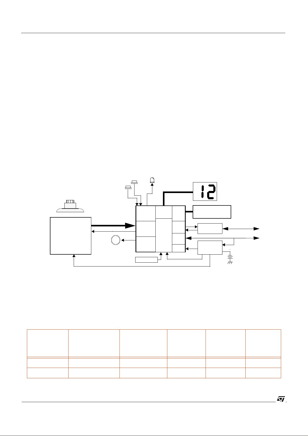
Push buttons:
Shutte r
Mode
Optional
LED Indicator
Optional
2 x 7 seg. LC D
Low cost lens
16MBit or 64MB it
SDRAM
Transceiver
Circuit
Power
ement
Mana
Circuit
RS232 interface
to PC
USB interface
to P C
6-9V Battery e.g., PP 3 ,
4-6 x AA, AAA, etc
CMOS Sensor:
VV6444/6410
CIF
VV6500
VGA
LCD
GPIO
Driver
memor
I/F
Sensor data
Sensor clock
Optional
Piezo
Buzzer
Mini
speaker
Switched sensor supply (5V for VV6444, 3v3 fo r VV6410/6500
Buffer Amp
Sensor
I/F
PWM
Audio I/F
12MH z XTAL
STV0680A
RS232
I/F
USB
I/F
Detect Low
Batter
3v3 supply (STV0680A
Figure 1 : Typical camera system block diagram
1.2 Co-processor choices
The following co-processor choices are available. The STV0680A supercedes STV0680, and uses different silicon and different
firmware compared to STV0680. Functionally it is exactly the same as STV0680 except that it supports a VfW driver. In addition,
a new firmware variant means that the STV0680A also supports VV6410 and VV6500 sensors, as well as 64Mbit memory size.
The firmware variant of STV0680 denoted by STV0680-001 does not support RS232 interface.:
Co-
processor
Sensors
supported
SDRAM
supported
USB
interface
RS232
interface
Video for
Windows
support
This version: ST VIBU internal use only
STV0680-001 VV6444 16Mbit onl
Yes No No
STV0680A-002 VV6444/6410/6500 16Mbit or 64Mbit Yes Yes Yes
Table 1 : Product choices
7
STV0680F_contents.fm
CDSTV0680F-C
Commercial in confidence
Page 8

PRELIMINARY
)
)
(
)
Digital Camera Chipset; Customer Datasheet, Rev 3.0,
March 2000
1.3 Sensor choices
The following sensors are supported:
Sensor Resolution
Sensor supply
VV6444 CIF (352 x 288
VV6410 3.3v
VV6500 VGA
640 x 480
Table 2 : Sensor choices with STV0680/STV0680A
1.4 Key system features
The key features of a typical camera based on the STV0680A chipset are as follows:
1.4.1 Image features (
• Support for 5V or 3.3V CIF resolution sensor (VV6444 or VV6410) - 352 x 288 pixels
• Support for 3.3V VGA resolution sensor (VV6500) - 640 x 480 pixels
• 80 picture storage capacity possible for CIF, with 64MB memory
STV0680A-002
STV0680A + VV6444/6410/6500
voltage
5v
• 26 picture storage capacity for VGA, with 64MBit memory
• A greater numbe r of images can be stored when ‘Low’ resolution mode is enabl ed (e.g. 80 QCIF images with 16M bit memory,
106 QVGA images with 64Mbit memory). See Table 4 and Table 5.
• Automatic anti-flicker exposure and gain control
1.4.2 Image features (
• Supports 5V CIF resolution sensor (VV6444) - 352 x 288 pixels.
• 20 picture storage capacity possible for CIF with 16MB memory.
• 80 picture storage capacity possible for QCIF with 16MB memory.
• Automatic anti-flicker exposure and gain control
STV0680-001
)
1.4.3 User features on camera
• Self-timer mode allows a picture to be captured after several seconds.
• Twin 7 segment LCD panel supported - showing number of pictures left, and modes.
• Picture counter helps the user to know how much memory is left.
• Un-tethered ‘Conti nuo us’ mode a llo ws captu re of ima ge sequ ences for storag e in memory and sub seque nt dow nload to PC.
• Piezo buzzer indicates a number of useful events to the user, e.g. whether enough light is present for picture capture, etc.
• Indicator LED.
This version: ST VIBU internal use only
1.4.4 User features on PC software
PC software allows a number of features, including fast download of thumbnail images for picture selection, and automatic
detection and correction of sensor defects. Table 3 clarifies the driver compatibility available, including:
• TWAIN driver to suit all TWAIN compatible imaging applications
• Video for Windows d river for tet hered video m ode (throug h USB), a va ilab le at all res olutions , with f as test fram erates at QCIF
resolution
CDSTV0680F-C
STV0680F_contents.fm
Commercial in confidence
8
Page 9

PRELIMINARY
STV0680A + VV6444/6410/6500 Digital Camera Chipset; Customer Datasheet, Rev 3.0,
• AVI video file creation from image sequences captured in ‘continuous’ mode
Interface type:
PC Operating system:
STV680-001 Not available TWAIN
STV0680A-002 TWAIN TWAIN, VfW
Custom OEM softwa re can be de velop ed by usin g t he SDK (fo r SDK a vaila bility , con tact S T), t o uplo ad thu mbnai ls/st ill im ages or
‘continuous’ images, e.g. for AVI file creation.
Win9x, WinNT4, Win2k
RS232
Table 3 : Driver choices
USB
Win98 and Win2k only
March 2000
1.4.5 Power management features and USB compliance
• Picture retention with extremely low power operation, which appears to the user as if the camera is “switched off”.
• Auto power-off after 30sec with no user activity
• Operates from 6-9V battery, although system voltage is 5V or 3.3V, dependant on sensor.
• Low battery detection
• Dependant on ha rdware configura tion, switc h-over to USB powe r supply is su pported, to all ow the devic e to operate wi th low
batteries or without batteries, when connected to USB.
• Full USB compl iance re quirement s are lis ted in the USB spe cification, however , in a ca mera d esigned u sing this c hipset, the
following must at least be inclu ded: (a) an SDRAM with sufficiently low self-r efresh current, (b) USB inrush protectio n circuitry,
and (c) (in the case of VV6444 only) a switched 5V sensor supply is used, to maintain sufficient supply voltage to the 5V
sensor. See Section 9. for further details.
1.4.6 General features
• High speed picture download over USB
• ST Colour processing algorithms available under license (as part of drivers/SDK)
• USB or RS232 serial interface options, and VfW / TWAIN driver support.
• Customisation of STV0680A is possible to vary the features described in this document, subject to commercial agreement
with ST, see Section 6.
This version: ST VIBU internal use only
9
STV0680F_contents.fm
CDSTV0680F-C
Commercial in confidence
Page 10
PRELIMINARY
Digital Camera Chipset; Customer Datasheet, Rev 3.0,
March 2000
STV0680A + VV6444/6410/6500
2. Detailed features
2.1 Sensor type and image formats
The sensor type is auto-detected by STV0680A, which ensures that the correct sensor timing is enabled, and the correct image
resolutions are enabled, as shown in Table 4.
For stills photo grap hy , ‘ High’ or ‘Low’ reso lu tion m od e can be selected, t o give CIF or QCIF pi ct ures from a CIF sens or, an d VGA
or QVGA from a VGA sensor (see Table 4 and Section 3.7). Reduced resolution allows for storage of more images. Images
captured in both ‘High’ and ‘Low’ resolution can be stored in camera memory at the same time. Therefore there is no need for
images stored in memory to be cleared before changing image resolution.
Where USB is connected, the host PC software (through a Video for Windows driver) can activate tethered video mode,
regardless of the user inputs to the camera buttons. In this case, the image resolution is controlled by the PC driver..
Sensor
VV6444/
6410
Max. no. of
Sensor
Image Size
Resolution
mode
Final Image Size
images
stored in
16MBit
memory
CIF 352 x 288 High CIF 352 x 288 20 80 9 frames/sec
Low QCIF 176 x 144
(Subsampled)
80 320
Max. no. of
images
stored in
64MBit
memory
(see notes)
Approximate
VfW framerate
(*)
25 frames/sec
VV6500 VGA 640 x 480 High VGA 640 x 480 (6) 26 2 frames/sec
Low QVGA 320 x 240
(Subsampled)
Table 4 : Image modes supported (
*Notes:
1. VfW framerate is dependant on PC performance and USB bus loading
2. Not all image sizes are supported by all STV0680/680A variants - see Table 2 for clarification.
3. A CIF camera with STV0 680A-002 and 64Mbit SDRAM can stor e up to 320 im ages b y using QC IF mode. Whe re >99 im ages
are still available, the LCD display will remain at 99. Where (no. of images available) <99, the LCD display will show the
number of images available, as is the case with all other modes.
(24) 106 12 frames/sec
STV0680A-002
)
Max. no. of
Sensor
Sensor
Image
Size
Resolution
mode
Final Image Size
images
stored in
16MBit
memory
VV6444 CIF 352 x
288
High CIF 352 x 288 20
Low QCIF 176 x 144
(Subsampled)
80
This version: ST VIBU internal use only
Table 5 : Image modes supported (
STV0680-001
)
2.1.1 VV6444
VV6444 is a CIF resolution, 5V CMOS imaging sensor. A brief specification is shown in Section 7. VV6444 has the same
functionality and array size as the un-microlensed VV6404 sensor, but has a microlensed array and different colour
characteristics. Although the VV64444 and VV6404 are electrically identical, the STV0680 and STV0680A use the correct
CDSTV0680F-C
STV0680F_contents.fm
Commercial in confidence
10
Page 11

PRELIMINARY
STV0680A + VV6444/6410/6500 Digital Camera Chipset; Customer Datasheet, Rev 3.0,
settings for the VV6444 colour set. This means that a VV6404 should not be used with STV0680/680A.
For IR filter design, the best choice filter follows the GS0034 dielectric stack filter specification, which is available from ST. An
alternative, although not optimal filter, would be Schott S8612 doped glass, also sold as CM500.
March 2000
2.1.2 VV6410
VV6410 is a CIF resolution, 3.3V CMOS imaging sensor. A brief specification is shown in Section 7.
A dual design to support VV6444 and VV6410 is not possible, since VV6410 is a 3v3 sensor. A dual footprint for VV6410 and
VV6500 is not possible since the package types differ, however, the same support circuit is used. See Section 9.
2.1.3 VV6500
VV6500 is a VGA resolution, 3.3V CMOS imaging sensor. A brief specification is shown in Section 7.
A dual design to support VV6444 and VV6500 is not possible, since VV6500 is a 3v3 sensor. A dual footprint for VV6410 and
VV6500 is not possible since the package types differ, however, the same support circuit is used. See Section 9.
2.2 User interface
The user interface supported by STV0680A comprises of user controls, audible signals and visual displays.
! Note
The precise functionality of the
version shown here is close to the actual functionality available in STV0680A.
user interface
may vary from that of existing demonstration units. The
2.2.1 Push buttons
The following are typical of the type of funct ions whic h are supported by the chipset. Th ese functio ns are achie vable wit h no more
than 2 push buttons.
1. Mode button (Wake-up/Switch between modes)
when the camera is to be used for taking pictures, or (1.2) to switch between modes of operation shown in Section 3..
2. Shutter button (Shutter/confirm action): This button allows the user to take a picture or confirm an action, as shown in Section 3.
The modes of operation are described in Section 3.
: This button al lows th e user (1.1) t o wa ke the c amera u p from sta ndby mode
2.2.2 LED indicator
An LED display camera status, i.e. to show that the camera is in ‘Snapshot’ mode.
2.2.3 Picture counter using 2 x 7 segment display
STV0680A stores a picture counter value, which shows how many images can still be captured. STV0680A supports a 2x7
segment LCD panel. In ‘Snapshot’ mode and continuous capture mode, this LCD panel displays the number of pictures still
available, which is useful to identify when the user is approaching the maximum number of images which can be stored (see
Table 4 and Table 5). It is possible to clear the images stored in memory, in order to continue taking pictures, as shown in Table
6. In other modes, this LCD panel shows displays a 2-character code as shown in Table 6, which helps the user to navigate
around the modes.
Note
: A CIF camera with STV0680A-002 and 64Mbit SDRAM can store up to 320 images by using QCIF mode. Where >99
images are still available, the LCD display will remain at 99. Where (no. of images available) <99, the LCD display will show the
number of images available, as is the case with all other modes.
This version: ST VIBU internal use only
For suitable numeric LCD panel types, see Section 4.8.
2.2.4 Piezo buzzer
An on-chip Pulse Width Modulator (PWM) on STV0680A is used to generate buzzer sounds to signal certain events. The
following are typical of the type of events which are indicated by the buzzer, and each has its own distinctive sound:
1. Camera has been ‘Woken up’ from standby mode (either b y th e us er pres s ing a b u tton , by re-connecting the power source,
or by connecting a USB/RS232 connection).
11
STV0680F_contents.fm
CDSTV0680F-C
Commercial in confidence
Page 12

PRELIMINARY
Digital Camera Chipset; Customer Datasheet, Rev 3.0,
2. Camera has been ‘gone to sleep’ i.e. moved into standby mode. Pictures are retained in memory.
3. Picture has been successfully taken after the user presses the capture button.
4. Picture has NOT been taken after the user presses the capture button. This indicates to the user that there is insufficient
light, or that the exposure control was not ready due to a rapid change of lighting in the scene.
5. Picture has NOT been taken after the use r p r ess es th e c apture button, due to picture counter having reached the m axi mum
number of images. The user has the chance to zero the counter if desired.
6. End of continuous capture in un-tethered ‘Continuous’ mode, due to memory full.
7. Self-timer activated and counting down.
March 2000
STV0680A + VV6444/6410/6500
2.3 Battery Level Detect and USB auto-switch
An on-chip battery level detector on STV0680A detects when the battery voltage falls below a threshold. This threshold is
determined by the designer, dependant on the perception of what remains as ‘acceptable’ image quality as the battery voltage
falls. The chos en th res hol d level is determi ne d by a resistor va lu e, as s how n i n Se ction 9. Where no USB has been de tec ted, the
LCD display flashes, which indicates that the battery is low. Where a USB connection has been detected, the camera sources
power from USB, if certain additional hardware is fitted.
Note
: It may be a requirement of certain USB compl iance tests tha t such additi onal ha rdware is in cluded in the camera design, in
order to enable the camera to switch to supply from USB and hence report back to the PC while connected to the USB bus
without a battery.
2.4 PC interface options and software support
Either USB Interface (full speed 12Mbit/sec max.) or RS232 interface (115.2Kbaud) is supported by the chipset, with driver
software available from ST for both. The interface type is auto-detected by the chipset. PC software can be one of the following
(exact compatibility is clarified in Table 3):
1. Simple image upload demonstration software supplied by ST, allowing uploading of stills or ‘continuous’ images. This software should not be supplied as an end-user product.
2. TWAIN driver to suit all TWAIN compatible imaging applications
3. Video for Windows driver for tethered video mode (USB only)
4. Custom end-user soft ware developed by O EM u sin g SD K (for SDK a vailability, contact ST). The SDK is sup pl ied by ST as a
32-bit DLL f ormat, running on Windo w s 98, a nd ac cess ed throu gh a do cume nted s oftw are i nterface. This pro vide s the b asis
for developing a custom software application for uploading stills and/or video. See Section 5. for further details.
2.4.1 USB
Complete images (displayed as either thumbnails or in full resolution), or the entire SDRAM contents (e.g. for uploading
continuously captured image sequences, recorded using ‘Continuous Capture’ mode) can be downloaded through USB, and
USB connection also allows for tethered video mode to be activated by the USB driver.
Thumbnail image download is extremely fast for the entire memory contents in the camera. Once a picture is selected for
download, full image download takes approximately 0.15 seconds per image for a CIF image (0.6 seconds for a VGA image),
plus post processing time per image.
For USB interface details, see Section 4.4.
Note
: Actual USB download and post processing time also depends on PC performance and USB bus loading
2.4.2 RS232 (not available on STV0680-001)
Thumbnails of images, complete stored images, or the entire SDRAM contents can be downloaded through RS232, but tethered
video is not supported.
Once a picture i s selec ted for down load, full im age d ownloa d take s a pproxi matel y 10 s econ ds pe r imag e for a CIF ima ge (arou nd
30 seconds for a VGA image), plus post processing time per image (of the order of 1 second approximately).
This version: ST VIBU internal use only
For RS232 interface details, see Section 4.5.
Note
: Actual post processing time after RS232 download also depends on PC performance
2.5 Anti-flicker exposure and gain control
The chipset operates automatic exposure and gain control for either 50Hz or 60Hz mains-driven indoor lighting, using the same
12MHz crystal. This improves picture quality by selecting a set of exposure values which minimise ‘flicker’ effects. Detection of
CDSTV0680F-C
STV0680F_contents.fm
Commercial in confidence
12
Page 13

PRELIMINARY
STV0680A + VV6444/6410/6500 Digital Camera Chipset; Customer Datasheet, Rev 3.0,
the mains frequency is dependant on the status of the GPIO3 pin, which can be achieved by population of a PCB link at a late
stage in production, once the country of destination is known, without the need to change the crystal frequency.
The auto exposure and gain algorithm is always enabled during ’Snapshot’/self-timer/continuous mode. When the shutter button
is pressed in ‘Snapsh ot’ mode, th e ch ipset capt ures an im age if th e expos ure and gain val ue has re ached a suitab le valu e for th e
current scene. If the light detected has suddenly changed, the camera may emit an audible tone to indicate that more time is
required to reach the correct exposure target. In ‘Snapshot’ mode the chipset only captures the image data if sufficient light is
present in the image. In continuous capture mode, the chipset captures images regardless of whether enough light is present.
Note
: Auto-detect of the mains lighting frequency is not currently supported.
March 2000
13
STV0680F_contents.fm
This version: ST VIBU internal use only
CDSTV0680F-C
Commercial in confidence
Page 14
PRELIMINARY
(
g
Digital Camera Chipset; Customer Datasheet, Rev 3.0,
3. Camera modes of operation
Mode
Standby
mode
’Snapshot’
mode
Continu-
ous cap-
ture
Self timer Takes one pi cture after a 10 second co unt-
’Clear
camera’
If shutter button pressed while in
this mode
No function - pictures cannot be taken in
standby mode
Takes one picture, if sufficient light availa-
ble, then returns to ‘Snapshot’ mode
Takes a picture every 80mS while button
pressed, regardless of light available, then
returns to ‘Snapshot’ mode
down, if sufficient light available, then
returns to ‘Snapshot’ mode
(1st press:)
Prompts user to
clear camera
2nd press:) Clears all
ima
es stored in cam, then returns to
era
‘Snapshot’ mode
pressed while in this
Moves to continuous cap-
Moves to self timer mode Returns to
Moves to ‘Clear camera’
Moves to ‘Change resolu-
March 2000
If mode button
mode
Wakes up camera into
‘Snapshot’ mode
ture mode
mode
tion’ mode (see note)
STV0680A + VV6444/6410/6500
If no further
action
Remains in
standby mode
Stays in ‘Sna p-
shot’ mode for
30 seconds then
moves to
standby mode
‘Snapshot’ mode
after 5 seco nds
LCD
displays
(Display is
blank)
Number of pictures still avail-
able to take
Number of pictures still avail-
able to take
“St”
“CL”
’Change
resolution’
Changes resolution
High to Low) and return s to ‘Snapshot’
(i.e. Low to High, or
mode
Returns to ‘Snapshot’
mode
If currently in
Low Resolu-
tion: “Hr”
If currently in
High resolu-
tion: “Lr”
Table 6 : Camera modes
Note: In STV0680-001, pressing the Mode button while in ‘Clear Camera’ mode only moves onto ‘Change resolution’ mode if the
camera has no images stored. This is because in STV0680-001, mixed resolutions (i.e. ‘High’ and ‘Low’) cannot be stored at the
same time. In STV0680A-002, mixed resolutions can be stored at the same time.
The above modes are interrupted by the detection of a USB or RS232 connection. This is to allow for the possibility that the PC
driver takes control of the chipset (e.g. when starting a VfW application through USB).
3.1 Standby mode (or USB suspend mode)
3.1.1 Entering this mode
The camera enters st and by mo de aut omati cally af ter 3 0 secon ds of inacti vity if not tethere d to USB, or w hen USB suspe nd mode
is activated by the PC driver.
3.1.2 Description
This allows image data to be stored in memory with extremely low power consumption, which appears to the user as if the
camera is switched ‘off’, since there is no LCD display or LED lit. In VV6444-based designs, STV0680A powers off the sensor
completely, in VV6410/6500 based designs, the sensor is placed in suspend mode, and the camera enters a mode where only
SDRAM refresh is carried out. The shutter button is inactive in standby mode.
This version: ST VIBU internal use only
3.1.3 Exiting this mode
Wake-up from standby mode is achieved by any of the following means:
1. Pressing the ‘mode’ button (only if no USB detected)
CDSTV0680F-C
STV0680F_contents.fm
Commercial in confidence
14
Page 15

PRELIMINARY
)
STV0680A + VV6444/6410/6500 Digital Camera Chipset; Customer Datasheet, Rev 3.0,
2.
RS232 receives start bit from host software
3. USB connection detected
4. If in USB suspend mode, U SB driver re-starts communications with the camera as per USB specification
(only if no USB detected
March 2000
3.2 ‘Snapshot’ mode (in High or Low resolution)
3.2.1 Entering this mode
This is the default mode on wake-up when not tethered to the PC, i.e. pressing the Mode button while in standby mode, or
powering up the camera. On entering this mode, the current resolution (i.e. ‘Hr’ or ‘Lr’) is displayed briefly, and there is a brief
pause (approx. 1second) during which pictures cannot be taken. This is to allow the Auto-exposure and Gain control to settle.
The LCD then displays the number of pictures still available.
3.2.2 Description
Using the shutter button, ‘Snapshot’ mode allows single pictures to be grabbed using the capture button. The LCD displays the
number of pictures still available. Auto-exposure and gain are continuously enabled. The camera grabs an image when the
capture button is pressed, if sufficient light is available, the exposure and gain algorithm is settled, and picture counter has not
reached it s
maximum. Image data is stored in memory and picture counter is decremented.
3.2.3 Exiting this mode
After 30 seconds of non-activity, while not tethered to the PC, the camera goes into Standby mode.
3.3 ‘Continuous Capture’ mode (in High or Low resolution)
3.3.1 Entering this mode
Enabled using the mode button (from ‘Snapshot’ mode, press once).
3.3.2 Description
The LCD displays “Ct”. Auto-exposure and gain are continuously enabled. While the shutter button is pressed, the user can
activate continuous capture at approx. 12.5 frames per second, to allow recording of a ‘video’ sequence, whether or not the
camera is tethered to the PC, and regardless of whether enough light is available. The picture counter is decremented once per
frame. The continuous image data is stor ed in memor y and can then be downloa ded to the PC. Once the memory is fu ll, the user
is alerted by an audible tone. It is possible to store a mixture of still images and ‘Continuous’ images in memory.
3.3.3 Exiting this mode
After 5 seconds of non-activity, or after releasing the shutter button, the camera returns to standby mode.
3.4 Self-timer Mode (in High or Low resolution)
3.4.1 Entering this mode
Enabled using the mode button (fro m ‘Snapshot’ mode, press twice).
3.4.2 Descript ion
The LCD displays “St”. Auto -exposure and gain are co ntinuous ly enable d. When the shut ter button is pressed, t he camera cou nts
down 10 seconds, then grabs an image, if sufficient light available and exposure and gain algorithm settled, and picture counter
has not reached its
maximum. Image data is stored in memory and picture counter is decremented.
This version: ST VIBU internal use only
3.4.3 Exiting this mode
After 5 seconds of non-activity, or after the timer has counted down 10 seconds, the camera returns to standby mode.
3.5 ‘Clear camera’
3.5.1 Entering this mode
Enabled using the mode button (from ‘Snapshot’ mode, press three times).
15
STV0680F_contents.fm
CDSTV0680F-C
Commercial in confidence
Page 16

PRELIMINARY
Digital Camera Chipset; Customer Datasheet, Rev 3.0,
March 2000
STV0680A + VV6444/6410/6500
3.5.2 Description
The LCD displays “CL”. Pressing shutter button twice will clear all the images in the camera.
3.5.3 Exiting this mode
After 5 seconds of non-activity, or after the camera has been cleared, the camera returns to standby mode.
3.6 ‘Change resolution’
3.6.1 Entering this mode
This is enabled using the mode button (from ‘Snapshot’ mode, press four times).
Note: In STV0680-001, the images stored in memory must be cleared before this mode can be entered. This is because in
STV0680-001, mixed resolutions (i.e. ‘High’ and ‘Low’) cannot be stored at the same time.
3.6.2 Description
The LCD displays the target resolution to which the camera can be changed, i.e. if in High resolution “Lr” (Low resolution) is
displayed, if in Low resolution, “Hr” (High resolution) is displayed. ‘High’ resolution stores the full image resolution from the sensor
array, while ‘Low’ subsamples the sensor array, to store 4x the number of images (e.g. 80 in QCIF mode, compared to 20 in CIF
mode).
Dependant on the type of s en sor us ed, diff eren t res ol uti ons are obt ained, see Table 4 or Tab le 5 . By pres s ing the sh utte r but ton,
user changes the resolution.
3.6.3 Exiting this mode
After 5 seconds of non-activity, or after the resolution has been changed, the camera returns to standby mode.
3.7 Tethered USB Video mode
3.7.1 Entering this mode
This is activated by the PC Video for Win dows driv er w hi le the cam era is tethered, dependant on whethe r VfW is supp orte d (se e
Table 3).
3.7.2 Descript ion
The camera is controlled by the PC driver.
Note: Any images or continuous image sequences contained in the camera are lost when the video for Windows driver starts.
3.7.3 Exiting this mode
This is controlled by the PC drivers.
3.8 Powering the camera off
3.8.1 Entering this mode
This is not truly a mode of operation, but a description of what happens if:
• The battery power and USB connection are removed from the camera
• The battery power is removed, and the PC to which the camera is tethered, is switched off.
This version: ST VIBU internal use only
• The battery v olt age falls extremely low. Ways of a vo idi ng this situation a re discussed in th e reference design, see Section 9 .
Note: normally a camera with U SB in terfa ce sho ul d so urc e po wer fro m th e USB connection, but this is hard ware dep end ant, see
Section 9.
3.8.2 Description
In this situation, all image data is lost.
Note: under certain circumstances, the image data may be maintained if the camera or PC is powered on again after a few
16
STV0680F_contents.fm
CDSTV0680F-C
Commercial in confidence
Page 17

PRELIMINARY
STV0680A + VV6444/6410/6500 Digital Camera Chipset; Customer Datasheet, Rev 3.0,
seconds, although this is not guaranteed).
March 2000
3.8.3 Exiting this mode
When the camera is pow ered on again, ei ther when the battery is re-f itted, or t he USB is re-connec ted, or the PC is re-started, the
camera will power up into standby mode, High resolution, with all images available.
17
STV0680F_contents.fm
This version: ST VIBU internal use only
CDSTV0680F-C
Commercial in confidence
Page 18
PRELIMINARY
y
Digital Camera Chipset; Customer Datasheet, Rev 3.0,
March 2000
STV0680A + VV6444/6410/6500
4. STV0680A hardware interfaces
4.1 STV0680A pinout
The STV0680A pinout has been carefully developed to minimise the physical size of the support printed circuit board by
facilitating placement of and electrical routing to peripheral support components such as the SDRAM. The complete pinout and
listing is shown in Section 8.
4.2 Sensor interface
STV0680A uses a standard ST digital interface from the sensor, and the sensor clock input is provided by an output from
STV0680A. Designing a camera using this chipset should design as close as possible to the reference design (Section 9.), in
which case the chipset can be regarded as a functional ‘bla ck box’, and no further details regar ding the STV0680A-sensor
interface are required.
4.3 Memory interface
STV0680A is designed to in terfa ce to an ex te rnal 16 Mb it or 64Mbit SDRAM (see Ta ble 4 and Table 5). The SDRAM device mu st
have a 16 bit wide data bus and op erate from a 3.3V sup ply. Two si zes of SD RAM memory are suppor ted by STV068 0A, 16MBits
(1M x 16 bits wide) or 64MBits (4M x 16 bits wide), the memory size is auto-detected by STV0680A. STV0680A clocks the
SDRAM at 6MHz, typica lly thi s i s well below the figures offered by most manufactu rers ’ de vic es . D ev ic es whic h are PC 66 a nd/o r
PC100 compliant are preferred. For interface wiring, see Section 9.
4.3.1 SDRAM Current consumption
For maximum system battery li fe while no picture s are bein g taken, an d to assi st in mee ting require ments for U SB compl iance, an
SDRAM should be chosen with the lowest possible self refresh current specification. For suggested SDRAM part numbers, see
Section 9.
4.3.2 SDRAM interface timing requirements
The following timing diagrams should be referred to when selecting SDRAM other than those recommended in Section 9.
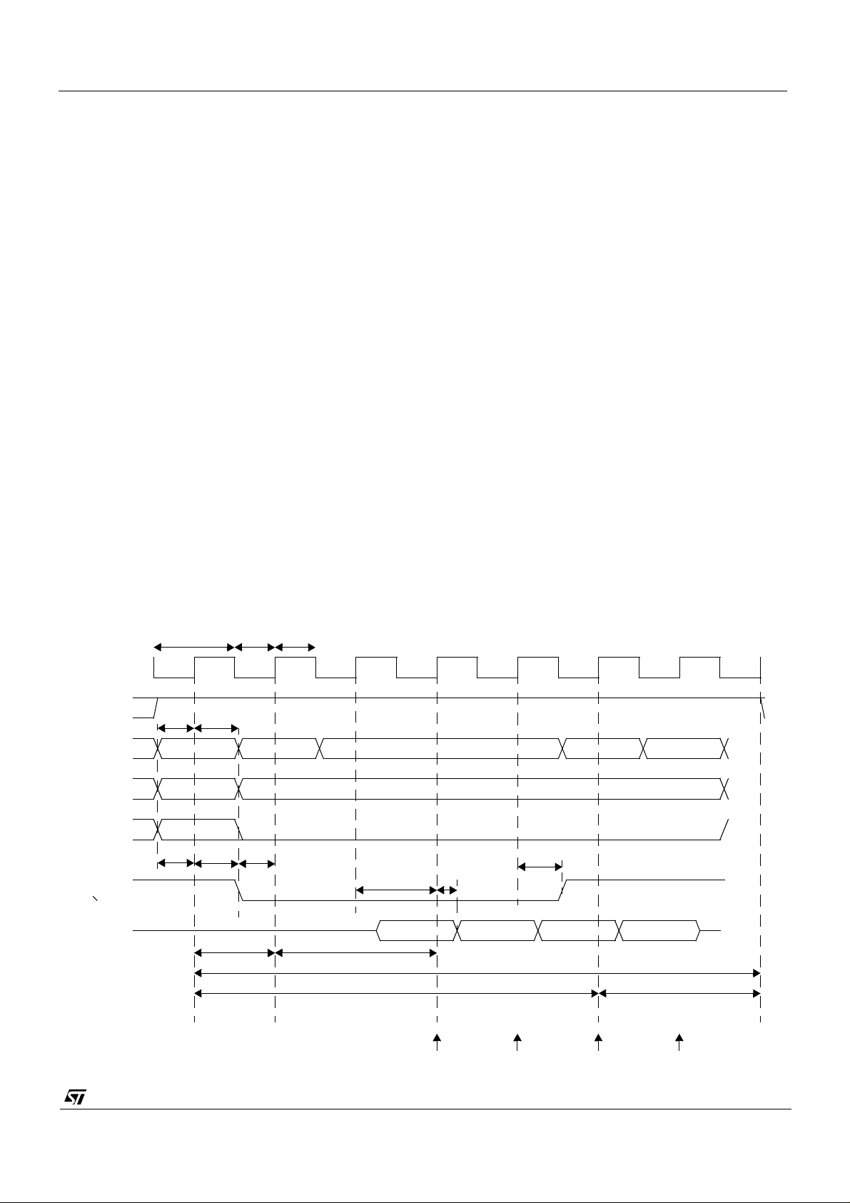
DCLK
CKE
Command
A0-9,BA
A10
DQM
DQ
t
CK
t
t
CMS
CMH
ACTIVE
ROW COLUMN
ROW
t
AS
t
t
AH
RCD
t
CMS
t
L
READ
t
H
READ Latenc
t
AC
DOUT M
t
RAS
NOP PRECHARGE NOP
t
CMH
t
OH
DOUT M + 1 DOUT M + 2 DOUT M + 3
t
RC
t
RP
This version: ST VIBU internal use only
STV0680F_contents.fm
DQ sample DQ sample DQ sample DQ sample
CDSTV0680F-C
Commercial in confidence
18
Page 19

PRELIMINARY
STV0680A + VV6444/6410/6500 Digital Camera Chipset; Customer Datasheet, Rev 3.0,
Figure 2 : SDRAM Read Timing (16Mbit device, burst read)
DCLK
CKE
Command
A0-9,BA
A10
DQM
DQ
t
CK
t
t
CMS
CMH
ACTIVE
ROW COLUMN
ROW
t
AS
t
t
L
H
WRITE
t
t
AH
CMS
DIN M
DIN M + 1 DIN M + 2 DIN M + 3
NOP PRECHARGE NOP
t
CMH
t
t
DH
DS
March 2000
t
RCD
t
RAS
t
RC
t
Figure 3 : SDRAM Write Timing (16Mbit device, burst write)
Symbol Min Max Units Symbol Min Max Units
t
CK
t
CH
t
CL
t
AC
t
OH
t
CMS
t
CMH
166.45 166.89 ns t
½tCKt
½tCKt
½t
CK
0nst
82.88 ns t
82.85 ns t
DS
DH
RCD
t
RAS
RC
RP
RCD
81.01 ns
83.41 ns
1t
55t
7t
2t
1t
CK
CK
CK
CK
CK
RP
This version: ST VIBU internal use only
t
AS
82.88 ns t
AH
82.76 ns
Table 7 : Timing parameters for SDRAM read/write
4.3.3 SDRAM refresh Period
The SDRAM refresh period from STV0680A is guaranteed to be no greater than 15.6µS during ‘Snapshot’/self-timer/continuous/
tethered video modes of operation (i.e. not standby mode). In standby mode, the SDRAM is set to self-refresh, therefore no
19
STV0680F_contents.fm
CDSTV0680F-C
Commercial in confidence
Page 20

PRELIMINARY
Digital Camera Chipset; Customer Datasheet, Rev 3.0,
refresh from STV0680A takes place.
March 2000
STV0680A + VV6444/6410/6500
4.3.4 SDRAM initialisation Period
The SDRAM initialisation period is currently set to 981µS in STV0680A.
4.4 USB interface
STV0680A includes a USB Version 1.1 compliant Universal Serial Bus Interface, including a transceiver. This allows direct
connection from STV068 0A to a USB conn ector w ith minim al addi tional hardwa re (i.e. a sm all nu mber of pa ssiv e disc retes) - se e
Section 9.
The USB interface interfaces the STV0680A to the USB at full speed 12MHz data rate. Some of the features are:
• Compliant with USB protocol revision 1.1.
• USB protocol handling.
• USB device state handli ng.
• Clock and data recovery from USB.
• Bit stripping and bit stuffing functions.
• CRC5 checking, CRC16 generation and checking.
• Serial to parallel conversion.
• Single bulk end point.
USB drivers are supplied by ST. For USB timing information, please refer to the USB specification V1.1.
4.5 UART module for RS232 interface
The UART module on STV0680A provides a 115200 baud full duplex interface to an external Host.
4.5.1 RS232 Physical interface
STV0680A does not support direct connection to a serial link. Physical line driver circuitry is required, e.g. using a standard
RS232 transceiver chip, or by using a small number of low cost discretes (as shown in Section 9.). The schematics shown
assume a 3 core cable with a length of no greater than 2m. Unscreened cable can be used, a suitable low cost connector is a
3.5mm audio jack plugs/sockets.
4.5.2 UART Module Overview
Receiving data
The UART module in STV0680A receives serial data through the RXD pin. Data reception is initiated by a 1-to-0 transition on
RXD, and the received data is sampled every 8.66µS.
If the RXD input is not 0 when the incoming data is first sampled, the UART module goes back to look for another 1-to-0
transition. This is to provide rejection of false start bits. If the start bit proves valid, reception of the rest of the frame will proceed.
Transmitting data
When a transmission is activated by STV0680A, the contents of an internal transmit shift register are shifted onto the TXD pin,
every 8.66µS.
The UART operates at 12MHz, which is not an integer multiple of 115200, so the actual baud rate is 115232 +/- 0.3%, which is
well within the requirements of a typical 16x oversampling UART, which can tolerate a 3.75% error in baud rate.
This version: ST VIBU internal use only
4.6 Power management and battery type
STV0680A and the SDRAM require a 3.3V supply. Where a VV6410 or VV6500 (3.3v) sensor is used, a single voltage regulator
can be used to regulate the sup ply for all three c ompon ents fro m the b attery, or the sens or on-bo ard VReg c an be us ed. Wh ere a
VV6444 is used, the sensor requires a 5V supply, hence a DC-DC converter is recommended to provide enough voltage when
the camera is powered from the USB bus. These are explained more fully in the reference design.
20
STV0680F_contents.fm
CDSTV0680F-C
Commercial in confidence
Page 21

PRELIMINARY
q
STV0680A + VV6444/6410/6500 Digital Camera Chipset; Customer Datasheet, Rev 3.0,
March 2000
4.6.1 Power switching to USB
Included in the USB compliance requirements, is the ability of the camera to report to the PC when connected to the USB bus,
whether or not
battery life while the camera is used in USB tethered video mode. In order to allow switching from battery to USB power, some
additional hardware is require d (see also Sect ion 9.):
• The USBDETECT input to STV0680A is used to detect that a USB power supply is connected
• If the USB is detected, additional hardware is used to switch off the battery
• An inrush protectio n circuit can protec t the USB bus from cur rent draw in the c ase of a low battery/ba ttery not fitted. Th is may
be necessary to comply with the USB specification.
• For precise USB compliance requirements, please consult the USB specification version 1.1
there is a fresh batte ry in the camera. This mea ns that pow er so urcing f rom U SB is requ ired, which also saves on
4.6.2 Switched sensor supply
Dependant on the hardware implementation, the SENSPWR output from STV0680A can be used to power off completely the
sensor during Standby mode (in the case of VV6444) or put the sensor into Suspend mode (in the case of VV6410/6500). This
has a significant improvement on battery life.
4.6.3 Battery type
This is hardware dependant. The schematics referred to in Section 9. assume either three or four 1.5V cells.
4.7 Quartz Crystal
Regardless of the sensor type or anti-flicker requirements, the sensor + STV0680A chipset operates from a single 12MHz
fundamental quartz crystal. For s pecificati on requirements, see Table 15. STV0680A includes an on-chip low jitter PLL, for PLL
characteristics, see Table 14.
4.8 Numeric LCD interface
STV0680A supports a 2-digit LCD panel only, for alpha-numeric display.
4.8.1 LCD types
STV0680A connects to a non multiplexed, direct drive LCD with 2 x 7 segments. Many LCD types are compatible with this
interface.
The LCD refresh fre
uency is 34.7Hz
.
4.8.2 LCD interface pinout
'0' connects to segmen t 'a', '1' c onnec ts to seg ment 'b' , and so on, wh ere a to g a re stand ard for all 7-segm ent dis play s, as w ell as
an LCD common output, giving
fifteen signals in total.
4.9 Switches and LED’s
The GPIO lines on STV0680A have pre-defined functions as fol lows , s ee Se ction 2.2 for user interface functionality, and Section
9. for precise hardware implementation.
! Note
The precise functionality of early demonstration units may vary from the actual user interface supported
by STV0680A.
4.9.1 MODE push button and SHUTTER push button: GPIO0 and GPIO1
Both push button inputs have internal de-bounce circuits, reducing the amount of hardware required externally. It is
recommended that labelling is used on the camera casing to help the user understand the functioning of the 2-button interface.
This version: ST VIBU internal use only
4.9.2 Input to select between 50 and 60Hz flicker frequency: GPIO3
This allows for factory setting of the anti-flicker frequency, dependant on the final country of destination. See also Section 2.5.
The polarity of this selection is detailed in the reference design (see Section 9.).
21
STV0680F_contents.fm
CDSTV0680F-C
Commercial in confidence
Page 22

PRELIMINARY
Digital Camera Chipset; Customer Datasheet, Rev 3.0,
4.9.3 LED indicator output: GPIO5
The LED output has an 8mA current sinking capability.
4.9.4 Unused pins: GPIO2, 4, 6, 7
These should be tied to GND.
March 2000
STV0680A + VV6444/6410/6500
STV0680F_contents.fm
CDSTV0680F-C
Commercial in confidence
This version: ST VIBU internal use only
22
Page 23

PRELIMINARY
)
g
)
g
g
g
g
STV0680A + VV6444/6410/6500 Digital Camera Chipset; Customer Datasheet, Rev 3.0,
March 2000
5. PC software
5.1 Driver support available
Interface type:
PC Operating system:
STV680-001 Not available TWAIN
STV0680A-002 TWAIN TWAIN, VfW
Win9x, WinNT4, Win2k
RS232
Table 8 : Driver choices
USB
Win98 and Win2k only
5.2 Demonstration software
The following is supplied with evaluation kits/demonstration units (This software is ma inly for demonstration p urpose s and s hould
NOT be supplied as an end-user product.
1. Simple demonstration software for uploading thumbnails and images.
2. Video demonstration application for STV0680-001 tethered “video” mode throu
. This is not required for STV0680A, which can be used with standard VfW drivers.
ble
3. AVI creator software for uploadin
! Note
With STV0680, a simple
sufficient framerate to allow for camera test, lens focussin
:
continuous images for creating ‘movie’ cli ps.
video.exe
application is provided. Whilst not being a VfW applic ation, it gives
, etc.
h USB (WIN 98 only) (NOT VfW compati-
5.3 OEM software
OEM’s have the following options for productisation of a camera based on the chipset:
1. TWAIN driver for uploadin
software.
2. Video for Windows driv er f or te the red v id eo m od e th rou
bundled with standard video for windows software.
3. Development of custom end-user software, including the ST colour process, developed under license using the SDK.
images, this would allow the camera to be bundled with standard TWAIN compatible imaging
h USB (WIN 98 & WIN2K only). This would allow the camera to be
5.4 Software Development Kit (SDK)
5.4.1 General
A software development kit is supplied by ST under license agreement, which allows the OEM to develop a custom application
which can perform picture download, thumbnail display, and colour processing. This supports Windows95TM (Serial interface
only) or Windows98/Win2KTM (Serial or USB), and includes features such as:
• Very fast download (through USB) and colour display of image thumbnails for picture selection
• Download of full image once selected by user software
• Colour processing of full image, using the ST colour process
• Automatic detection and correction of sensor defects
TM
The SDK is supplied by ST as a 32-bit DLL format, running on Windows 98/Win2K
software interface. This provides the basis for developing a custom software application for stills and/or video.
The ST SDK for the chipset comprises the following:
, and accessed through a documented
This version: ST VIBU internal use only
• Interface library containing all Application Programmer’s Interface (API) functions. Provided as C library and header files.
• All driver files necessary for chosen communications link (supplied as DLL and SYS files).
• Documentation of all API functions including example code fragments.
All software is built as 32-bit modules for Windows 98 /Win2K. The serial communications link is also supported for Windows 95.
A development environment of Microsoft Visual C++ v5 or higher is assumed.
23
STV0680F_contents.fm
CDSTV0680F-C
Commercial in confidence
Page 24

PRELIMINARY
Digital Camera Chipset; Customer Datasheet, Rev 3.0,
March 2000
STV0680A + VV6444/6410/6500
5.4.2 API Overview
All OEM application software communicates with the camera by means of the API as illustrated in Figure 4.
User Application
API
Drivers
Camera Module
Figure 4 : Software interface
The user application, API and drivers all run on the host PC. The drivers communicate with the camera by the chosen
communications link (either serial or USB). The core API functions allow for:
• The camera to be opened and closed as a device under the operating system
• Query of camera information and configuration (e.g., the number of pictures taken, current mode setting)
• Uploading of images and thumbnail images
• Control of camera functions (e.g., taking a picture or resetting the image counter).
Both single-threaded and multi-threaded programming models are supported and the camera may be accessed using either
synchronous (i.e., blocking) or asynchronous (i.e., non-blocking or overlapped) communications. Where asynchronous
communications are used, the application developer is responsible for coordinating tasks and access to the camera.
This version: ST VIBU internal use only
STV0680F_contents.fm
CDSTV0680F-C
Commercial in confidence
24
Page 25

PRELIMINARY
STV0680A + VV6444/6410/6500 Digital Camera Chipset; Customer Datasheet, Rev 3.0,
March 2000
6. Customisation options
The feature set of the STV0680A chipset encompasses the vast majority of digital stills and toy camera applications. However,
subject to comm ercia l agre ement for high vo lume app licat ion s, the c onfigu ratio n of S TV0680A could be modifie d by ST to a llo w a
new chipset to be produced.
Please contact ST for details.
25
STV0680F_contents.fm
This version: ST VIBU internal use only
CDSTV0680F-C
Commercial in confidence
Page 26

PRELIMINARY
Digital Camera Chipset; Customer Datasheet, Rev 3.0,
March 2000
STV0680A + VV6444/6410/6500
7. Detailed chipset specifications
7.1 Typical camera specifications
The following data assumes that the camera has been built according to reference design shown in Section 9.
Supply Voltage: 6-9V (when powered from battery) or 5V
(when powered from USB). (* See Note 1.)
o
Operating Temperature range 0
Example lens horizontal FOV 44
Max. RS232 cable length supported 2m
CIF output 352 x 288 pixels
QCIF output 176 x 144 pixels
VGA output (using VV6500) 640 x 480 pixels
QVGA output (using VV6500) 320 x 240 pixels
Image upload format Raw Bayer
PC driver output format Colour RGB bitmap
C - 40oC
o
(* See note 2)
Table 9 : Typical camera specifications
Notes:
1.Dual USB or battery power supply is only possible when the required power switching har dware is included, as shown in
Section 9.
2.Figures are approximate and depend on actual components sourced.
Sensor Min Max
VV6444 8.18µS39mS
VV6410 8.67µS44mS
VV6500 7.94µS66mS
Table 10 : Approximate shutter speeds
7.2 STV0680/STV0680A companion processor
Parameter Min Typ Max Units
Supply Voltage 3.0 3.3 3.6 V
This version: ST VIBU internal use only
Current consumption (normal operation) 20 TBD mA
Standby current consumption (untethered standby
mode or PC suspend mode)
Operating Temperature range 0 70
Package 100QFP
Exposure control 1 000 000:1
Table 11 : STV0680/STV680A Specifications
STV0680F_contents.fm
CDSTV0680F-C
Commercial in confidence
0.35 TBD mA
o
C
26
Page 27

PRELIMINARY
STV0680A + VV6444/6410/6500 Digital Camera Chipset; Customer Datasheet, Rev 3.0,
Description Range Unit
Storage Temperature
50 to 150
(Approximate)
Table 12 : STV0680/STV0680A Absolute Maximum Ratings
o
C
Parameter Description Min Typ Max Units
VDD Power Supply 3.0 3.3 3.6 V
V
V
V
V
V
TF
Z
V
V
V
V
R
R
TF
TF
ILU
IHU
IHUZ
DI
CM
OLU
OHU
OHU
CRS
PU
PD
R
F
RFM
DRV
USB differential pad D+/D- output signal cross over voltage 1.3 2.0 V
USB differential pad D+/D- input low 0.8 V
USB differential pad D+/D- input high (driven) 2.0 V
USB differential pad D+/D- input high (floating) 2.7 3.6 V
USB differential pad D+/D- input sensitivity 0.2 V 1
USB differential pad D+/D- common mode voltage 0.8 2.5 V 2
USB differential pad D+/D- output low voltage 0.0 0.3 V
USB differential pad D+/D- output high voltage 2.8 3.6 V
USB differential pad D+/D- output high voltage 2.8 3.6 V
USB differential pad D+/D- pullup resistor 1.425 1.575 KΩ
USB differential pad D+/D- pulldown resistor 14.25 15.75 KΩ
Rise Time 4 20 ns
Fall Time 4 20 ns
Differential Rise Time and Fall Time Matching 90 111.11 % 3
Driver Output Resistance 28 44 Ohms 4
March 2000
Note
s
Table 13 : STV0680/STV0680A DC Characteristics
Notes on Table 13:
1. VDI = |(D+) - (D-)|
2. VCM includes VDI range.
3. TF
4. Z
=( TFR / TFF ).
RFM
includes an external resistor of 20 Ohms serial to this transceiver.
DRV
Parameter Symbol Min Typ Max Unit Condition
Peak to peak jitters -- -- 170 220 ps @VCOfreq = 100MHz ~ 200MHz
Duty cycle -- 40 50 60 %
Operating voltage range VDD 3 3.3 3.6 V
Input low voltage VIL - 0.8 V VDD=3.3V
Input high voltage VIH 0.7VDD VDD V VDD=3.3V
Pull_in Time + Locking
Time
27
Tready -- -- 0.5 ms
CDSTV0680F-C
This version: ST VIBU internal use only
STV0680F_contents.fm
Commercial in confidence
Page 28

PRELIMINARY
Digital Camera Chipset; Customer Datasheet, Rev 3.0,
Output Slew Rate [ Tsr(Fout) -- 0.100+0.1082*CL -- ns CL:Output Load(pF)
March 2000
STV0680A + VV6444/6410/6500
Table 14 : STV0680/STV0680A PLL Characteristics
Parameter Min Typ Max Units
Crystal specification 50/50/10/30 (12mhz Fundamental)
Crystal frequency 12.000 MHz
Frequency tolerance 50 ppm
Temperature stability 50 ppm
Operating temperature -10 Deg. C
Load capacitance 30 pF
Table 15 : STV0680/STV0680A Crystal Tolerance
STV0680F_contents.fm
CDSTV0680F-C
Commercial in confidence
This version: ST VIBU internal use only
28
Page 29

PRELIMINARY
STV0680A + VV6444/6410/6500 Digital Camera Chipset; Customer Datasheet, Rev 3.0,
7.3 VV6444 Sensor
Colour Image Format 352 x 288 pixels (CIF)
Pixel Size 12.0 x 11.0µm
Image array size 4.272mm x 3.212mm
Array Fo rmat CIF
Sensor signal / Noise ratio Approx. 48dB (* See note 1)
Supply Voltage 5.0V DC +/-5%
Package type 48LCC
o
Operating Temp. range 0
Current consumption Min Typ Max Units
’Snapshot’/self-timer/continuous/tethered
video modes of operation
Standby/PC Suspend Mode, sensor pow-
ered off (see note 2)
Standby/PC Suspend Mode, sensor pow-
ered on (See note 3)
Negligible TBD µA
Approx.
C - 40oC
30 TBD mA
TBD µA
300
March 2000
Table 16 : VV6444 Specifications
* Notes:
1. 48dB refers to VV6404. With the addition of microlenses on VV6444, an increase in sensitivity can be expected.
2. Where the sensor is completely powered off by a FET or switcher (external hardware) during the Standby/PC Suspend
Mode.
3. Where the FET/switcher is not implemented, and the sensor is powered throughout Standby/PC Suspend Mode, however
the sensor clock is disabled.
Parameter Min. Max. Notes
V
IL
V
IH
V
OL
V
OH
TJ Junction Temp 0 deg C 100 deg C
Internal Pullup resistor 35kΩ 150kΩ
Internal Pulldown resistor 35kΩ 150kΩ
-0.5v 0.3 x V
0.7 x V
DD
2.4v VDD - 0.5v IOH = 100µA
VDD + 0.5v Guaranteed input high voltage
DD
0.4V At max IOL for pad type
Guaranteed input low voltage
At max I
Table 17 : VV6444 DC Characteristics
for pad type
OH
This version: ST VIBU internal use only
7.4 VV6410 and VV6500 sensors
Colour Image Format 352 x 288 pixels (CIF)
Pixel Size 7.5 x 6.9µm
29
STV0680F_contents.fm
Table 18 : VV6410 Specifications
CDSTV0680F-C
Commercial in confidence
Page 30

PRELIMINARY
Digital Camera Chipset; Customer Datasheet, Rev 3.0,
Image array size 2.67mm x 2.04mm
Array Format CIF
Sensor signal / Noise ratio Approx. 57dB
Package type 36LCC
Supply Voltage 3.3V DC +/-5%
Operating Temp. range 0
Current consumption: Min Typ Max Units
’Snapshot’/self-timer/continuous/tethered
video modes of operation
Standby Mode/PC Suspen d Mode, SUS-
PEND pin asserted (see note 1)
Standby Mode/PC Suspen d Mode, SUS-
PEND pin
not
asserted (see note 2)
Table 18 : VV6410 Specifications
Notes:
March 2000
STV0680A + VV6444/6410/6500
o
C - 40oC
25 TBD mA
<100 TBD µA
<300 TBD µA
1. Assuming appropriate external hardware recommendations are implemented (see Section 9.), the sensor SUSPEND pin is
asserted during Standby M ode /PC Su sp end M ode. Hence the s ens or is placed in Sen so r Su spend mode by m ea ns of (a) a
Serial interface message and (b) the SUSPEND pin being asserted.
2. Where the external hardware does not permit the sensor SUSPEND pin to be asserted during Standby Mode/PC Suspend
Mode, the sen s or is placed in Sensor Su spend mode by mean s of a Serial interface message only. This increases current
consumption due to a pull-up on the SUSPEND pin.
Colour Image Format 640 x 480 pixels (VGA)
Pixel Size 7.5 x 7.5µm
Image array size 4.89mm x 3.66mm
Array Format VGA
Sensor signal / Noise ratio Approx. 57dB
Supply Voltage 3.3V DC +/-5%
Package type 48LCC
o
Operating Temp. ra n ge 0
Current consumption: Min Typ Max Units
’Snapshot’/self-timer/continuous/tethered
video modes of operation
C - 40oC
30 TBD mA
This version: ST VIBU internal use only
Standby Mode/PC Suspend Mode, SUS-
PEND pin asserted (see note 1)
Standby Mode/PC Suspend Mode, SUS-
not
PEND pin
asserted (see note 2)
<100 TBD µA
<300 TBD µA
Table 19 : VV6500 Specifications
Notes:
1. Assuming appropriate external hardware recommendations are implemented (see Section 9.), the sensor SUSPEND pin is
CDSTV0680F-C
STV0680F_contents.fm
Commercial in confidence
30
Page 31

PRELIMINARY
STV0680A + VV6444/6410/6500 Digital Camera Chipset; Customer Datasheet, Rev 3.0,
asserted during Standby M ode /PC Su sp end M ode. Hence the s ens or is placed in Sen so r Su spend mode by m ea ns of (a) a
Serial interface message and (b) the SUSPEND pin being asserted.
2. Where the external hardware does not permit the sensor SUSPEND pin to be asserted during Standby Mode/PC Suspend
Mode, the sen s or is placed in Sensor Su spend mode by mean s of a Serial interface message only. This increases current
consumption due to a pull-up on the SUSPEND pin.
March 2000
Parameter Min. Max. Notes
V
IL
V
IH
V
OL
V
OH
TJ Junction Temp 0 deg C 100 deg C
Standard Pullup (SDA, SCL) 35µA current
Standard Pulldown (OEB) 25µA current
-0.5v 0.3 x V
0.7 x V
DD
2.4v VDD - 0.5v IOH = 100µA
draw
draw
VDD + 0.5v Guaranteed input high voltage
52µA current
42µA current
DD
0.4V At max IOL for pad type
draw
draw
Guaranteed input low voltage
At max I
for pad type
OH
Non-standard Pullup
(RESETB)
66µA current
draw
250µA current
draw
Table 20 : VV6410/6500 DC Characteristics
7.5 Typical current consumption of complete camera
The following data assumes that the camera has been built according to reference design referred to in Section 9. Figures are
approximate and depend on actual components sourced - see notes.
This version: ST VIBU internal use only
31
STV0680F_contents.fm
CDSTV0680F-C
Commercial in confidence
Page 32

PRELIMINARY
Digital Camera Chipset; Customer Datasheet, Rev 3.0,
7.5.1 Using VV6444 (sensor operates at @ 5V DC)
Mode
’Snapshot’/Cont inuous/
Self timer mode (while
un-tethered)
’Snapshot’/Continuous/
Self timer mode (while
tethered to PC)
Camera standby mode
(when NOT co nnected to
USB)
Suspend mode
(when connected to
USB)
Typical Current
Cons.
80mA
80mA Assuming appropriate hardware included, power is
Approx. 0.4mA +
SDRAM self-refresh
current (see note 2)
Approx. 0.6mA +
SDRAM self-refresh
current (see note 2)
Total current in this mode equals
STV0680/680A Standby current consumption (see note 1)
+ SDRAM self-refresh current (see note 2)
+ peripheral circuitry (approx. 50µ
Total current in this mode equals
STV0680/680A Standby current consumption (see note 1)
+ SDRAM self-refresh current (see note 2)
March 2000
STV0680A + VV6444/6410/6500
Comments
sourced from PC while USB connected.
:
:
A, see note 3).
+ peripheral circuitry (approx. 50
+ 200
A , based on 1.5k pull-up in camera (see Section
µ
9.) and 15k pull-down in PC.
A, see note 3).
µ
Table 21 : Current consumption, complete STV0680A+VV6444 camera
Notes:
1. See Table 11 on page26.
2. From li mited evaluatio n, typi cal se lf-refres h curre nt figu res of c ertain SDRAM chi ps are well b elo w m anu f act urers’ m axim um
specification, e.g. 100-250
3. This is assuming a low quiescent current 3v3 VReg is used, and assuming that the sensor is switched off using external circuitry.
A. See Section 9. for recommendat ions.
µ
This version: ST VIBU internal use only
STV0680F_contents.fm
CDSTV0680F-C
Commercial in confidence
32
Page 33

PRELIMINARY
STV0680A + VV6444/6410/6500 Digital Camera Chipset; Customer Datasheet, Rev 3.0,
7.5.2 Using VV6410/6500 (sensor operates at @ 3.3V DC)
Mode Typical Comments
’Snapshot’/Continuous/
Self timer mode (while
un-tethered)
’Snapshot’/Contin uou s/
Self timer mode (while
tethered to PC)
Standby Mode (when
NOT connecte d to USB):
Sensor SUSPEND pin
asserted (see note 4)
PC Suspend mode
(when connected to
USB): Sensor SUSPEND
pin asserted (see note 4)
60mA Assuming appropriate hardware included, power is sourced from PC
while USB connected.
60mA
Approx. 0.5mA +
SDRAM self-
refresh current (see
note 2)
Approx. 0.7mA +
SDRAM self-
refresh current (see
note 2)
Total current in this mode equals
STV0680A Standby current consumption (see note 1)
+ SDRAM self-refresh current (see note 2)
+ peripheral circuitry (approx. 50µ
+ Sensor suspend mode current (See note 3)
Total current in this mode equals
STV0680A Standby current consumption (see note 1)
+SDRAM self-refres h current (see note 2)
:
A).
:
March 2000
+ peripheral circuitry (approx. 50µ
+ 200
pull-down in PC.
+ Sensor suspend mode current (See note 3)
A , based on 1.5k pull-up in camera (see Section 9.) and 15k
µ
A).
Table 22 : Current consumption, complete STV0680A+VV6410/6500 camera
Notes:
1. See Table 11 on page page 26. However, STV0680A mean current consumption is to be determined by measurement of
sample quantity in due course.
2. From li mited evaluatio n, typi cal se lf-refres h curre nt figu res of c ertain SDRAM chi ps are well b elo w m anu f act urers’ m axim um
specification, e.g. 100-250
3. Sensor suspend mode current <100µ
4. If the appropriate hardware to asse rt the sensor SUSPEND pin is not fitted, an addditio nal current consu mption in thi s mode
of up to 200µA can be expected.
A. See Section 9. for recomm end atio ns.
µ
A when SUSPEND pin asserted, see Table 18 and Table 19.
This version: ST VIBU internal use only
33
STV0680F_contents.fm
CDSTV0680F-C
Commercial in confidence
Page 34

PRELIMINARY
Digital Camera Chipset; Customer Datasheet, Rev 3.0,
March 2000
STV0680A + VV6444/6410/6500
8. STV0680A Pin descriptions and Package Information
8.1 STV0680A Pin Listing
Pin no. Signal Type Description drive
Sensor Interface
69 SENSPWR Output, active high Power-up Sensor 2mA (SL)
68 SENSRST Output, active low Reset Sensor 2mA (SL)
60 SCL Input/Output (OD,T) Sensor serial interface 4mA (SL)
61 SDA Input/Output (OD,T) Sensor serial interface 4mA (SL)
62 SD3 Input (S,T) Sensor data
63 SD2 Input (S,T) Sensor data
64 SD1 Input (S,T) Sensor data
65 SD0 Input (S,T) Sensor data
66 QCLK Input (S,T) Qualification clock from sensor
67 SCLKO Output Clock output to sensor 4mA
GPIO (see note)
77 GPIO0 (MODE) Debounced input Push button (Wake-up/Mode) 8mA (SL)
76 GPIO1
(SHUTTER
75 GPIO2 IO (OD) Not used (tie to GND with 0R link) 8mA (SL)
74 GPIO3 (50/60) Debounced input Link to select between 50Hz and 60Hz lighting 8mA (SL)
73 GPIO4 IO (OD) Not used (tie to GND with 0R link) 8mA (SL)
72 GPIO5 Output (OD) LED indicator 8mA (SL)
71 GPIO6 IO (OD) Not used (tie to GND with 0R link) 8mA (SL)
70 GPIO7 IO (OD) Not used (tie to GND with 0R link) 8mA (SL)
42 USBDETECT Input (S) Detect Power source from USB.
43 DATA+ Input/Output USB bus
44 DATA- Input/Output USB bus.
)
Debounced input Push button (Shutter/Confirm) 8mA (SL)
USB Interface
USB speci-
(For camer a with R S23 2 only, this pin sh ou ld be tied t o GND )
(For camer a with RS232 on ly, this pin should be connected to
test points to allow for USB production test (lens focussing))
(For camer a with RS232 on ly, this pin should be connected to
test points to allow for USB production test (lens focussing))
RS232 Interface
fication
V1.1 com-
pliant I/O
This version: ST VIBU internal use only
58 TXD Output Serial data transmit
(For camera with USB only, this pin should be tied to RXD)
59 RXD Input (S) Serial data receive
(For camera with USB only, this pin should be tied to TXD)
STV0680A Master Clocks and Reset
48 XIN Input Quartz Crystal IN
49 XOUT Output Quartz Crystal OUT
CDSTV0680F-C
STV0680F_contents.fm
Commercial in confidence
4mA (SL)
34
Page 35

PRELIMINARY
STV0680A + VV6444/6410/6500 Digital Camera Chipset; Customer Datasheet, Rev 3.0,
March 2000
Pin no. Signal Type Description dr ive
51 RESET Input (S) Active (LOW) STV0680A reset
System Memory (SDRAM) Interface
20 DQMU Output Data i nput/output mask for dram_DQ[15:8] 2mA (SL)
22 DCLK Output Clock: all SDRAM input signals are sampled on the positive
edge
24 CKE Output Clock enable: activates (HIGH) and deactivates (L OW) the
SDRAM CLK signal
28 AD11 Output SDRAM address A11 for 64M SDRAM or BA for 16M
SDRAM
31 AD9 Output SDRAM address A9 2mA (SL)
33 AD8 Output SDRAM address A8 2mA (SL)
35 AD7 Output SDRAM address A7 2mA (SL)
37 AD6 Output SDRAM address A6 2mA (SL)
39 AD5 Output SDRAM address A5 2mA (SL)
41 AD4 Output SDRAM address A4 2mA (SL)
4mA
2mA (SL)
2mA (SL)
40 AD3 Output SDRAM address A3 2mA (SL)
38 AD2 Output SDRAM address A2 2mA (SL)
36 AD1 Output SDRAM address A1 2mA (SL)
34 AD0 Output SDRAM address A0 2mA (SL)
32 AD10 Output SDRAM address A10 2mA (SL)
26 AD12 Output SDRAM address A12, BA0 for 64M SDRAM, unused on 16M 2mA (SL)
30 AD13 Output SDRAM address A13, BA1 for 64M SDRAM, unused on 16M 2mA (SL)
25 CS Output, active low Chip select: enables (registered LOW) and disables (regis-
tered HIGH) the SDRAM command decoder.
23 RAS Output, active low SDRAM row address strobe command 2mA (SL)
21 CAS Output, active low SDRAM column address strobe command 2mA (SL)
19 WE Output, active low SDRAM write enable command 2mA (SL)
18 DQML Output Data input/output mask for dram_DQ[7:0] 2mA (SL)
16 DQ7 Input/Output SDRAM Data Bus 2mA (SL)
14 DQ6 Input/Output SDRAM Data Bus 2mA (SL)
12 DQ5 Input/Output SDRAM Data Bus 2mA (SL)
10 DQ4 Input/Output SDRAM Data Bus 2mA (SL)
8 DQ3 Input/Output SDRAM Data Bus 2mA (SL)
6 DQ2 Input/Output SDRAM Data Bus 2mA (SL)
2mA (SL)
This version: ST VIBU internal use only
4 DQ1 Input/Output SDRAM Data Bus 2mA (SL)
100 DQ0 Input/Output SDRAM Data Bus 2mA (SL)
2 DQ15 Input/Output SDRAM Data Bus 2mA (SL)
5 DQ14 Input/Output SDRAM Data Bus 2mA (SL)
7 DQ13 Input/Output SDRAM Data Bus 2mA (SL)
35
STV0680F_contents.fm
CDSTV0680F-C
Commercial in confidence
Page 36

PRELIMINARY
Digital Camera Chipset; Customer Datasheet, Rev 3.0,
March 2000
STV0680A + VV6444/6410/6500
Pin no. Signal Type Description dr ive
9 DQ12 Input/Output SDRAM Data Bus 2mA (SL)
11 DQ11 Input/Output SDRAM Data Bus 2mA (SL)
13 DQ10 Input/Output SDRAM Data bus 2mA (SL)
15 DQ9 Input/Output SDRAM Data bus 2mA (SL)
17 DQ8 Input/Output SDRAM Data bus 2mA (SL)
LCD Interface
85 LCDCOM Output LCD Common 2mA (SL)
93 LCD1_6 Output LCD digit 1 segment G 2mA (SL)
94 LCD1_5 Output LCD digit 1 segment F 2mA (SL)
95 LCD1_4 Output LCD digit 1 segment E 2mA (SL)
96 LCD1_3 Output LCD digit 1 segment D 2mA (SL)
97 LCD1_2 Output LCD digit 1 segment C 2mA (SL)
98 LCD1_1 Output LCD digit 1 segment B 2mA (SL)
99 LCD1_0 Output LCD digit 1 segment A 2mA (SL)
86 LCD2_6 Output LCD digit 2 segment G 2mA (SL)
87 LCD2_5 Output LCD digit 2 segment F 2mA (SL)
88 LCD2_4 Output LCD digit 2segment E 2mA (SL)
89 LCD2_3 Out put LCD digit 2segment D 2mA (SL)
90 LCD2_2 Out put LCD digit 2segment C 2mA (SL)
91 LCD2_1 Output LCD digit 2 segment B 2mA (SL)
92 LCD2_0 Output LCD digit 2 segment A 2mA (SL)
Piezo Interface
84 PIEZO Output Direct connection to piezo buzzer 8mA (SL)
Battery Level Comparator Interface
80 LO_BAT Input (A) Battery level comparator input. The voltage on low_bat is
compared to the reference to determine the battery status
79 LO_BAT_REF Input (A) 1.22V battery level comparator reference input
Power and Ground
1, 27, 50,
56, 78
3, 29, 57,
83
52 PLLGVDD Power pin PLL Guard Power
53 PLLGVSS Power pin PLL Guard Ground
DVSS[1-5] Power pin Digital Ground
DVDD[1-4] Power pin Digital Power
This version: ST VIBU internal use only
54 PLLAVDD Power pin PLL Analog Power
55 PLLAVSS Power pin PLL Analog Ground
Non-user pins
45 TEST0 Input Non-user pin - connect to 3V3
46 TEST1 Input Non-user pin - connect to 3V3
CDSTV0680F-C
STV0680F_contents.fm
Commercial in confidence
36
Page 37

PRELIMINARY
Digital Camera Chipset; Customer Datasheet, Rev 3.0,
March 2000
STV0680A + VV6444/6410/6500
Pin no. Signal Type Description dr ive
47 TEST2 Input Non-user pin - connect to 3V3
81 DACRES Non- user pin
I(A)
82 DACOUT Non-user pin
O (A)
DAC bias amplifier reference input
8-bit DAC current source output
Table 23 : STV0680A Pin listing
Key:
• SL - slew rate limited output
• OD - open drain output
• S - schmitt input
• A - analog input/output
• T - 5V tolerant pad (these pads do not have diode protection)
See example schematic in Section 9.
See example schematic in Section 9.
0-10mA (2)
Where the I/O pad type is not explicitly defined in the above notes, assume CMOS.
Note: GPIO are not ‘g ene ral purpose’, in the sense th at t hei r fu nc tio n i s pred ete r mi ned (e. g. GPIO0 = MODE, GPIO2 is Un use d),
dependant on the variant number of STV0680/STV0680A, denoted by the suffix on the part number -00x.
This version: ST VIBU internal use only
STV0680F_contents.fm
CDSTV0680F-C
Commercial in confidence
37
Page 38

PRELIMINARY
)
)
(
)
)
Digital Camera Chipset; Customer Datasheet, Rev 3.0,
8.2 STV0680A pinout diagram
DQ0
LCD1_a
LCD1_b
LCD1_c
LCD1_d
LCD1_e
LCD1_f
LCD1_g
LCD2_a
LCD2_b
99989796959493929190898887868584838281
100
DVSS1
DQ15
DVDD1
DQ1
DQ14
DQ2
DQ13
DQ3
DQ12
DQ4
DQ11
DQ5
DQ10
DQ6
DQ9
DQ7
DQ8
DQML
DQMU
CAS
DCLK
RAS
CKE
AD12
DVSS2
AD11
DVDD2
AD13
WE
CS
1
2
3
4
5
6
7
8
9
10
11
12
13
14
15
16
17
18
19
20
21
22
23
24
25
26
27
28
29
30
STV0680A
100QF P
March 2000
LCD2_c
LCD2_d
LCD2_e
LCD2_f
STV0680A + VV6444/6410/6500
LCD2_g
LCDCOM
PIEZO
DVDD4
DACOUT
DACRES
80
LO_BAT
79
LO_BAT_REF
78
DVSS5
77
GPIO0
76
GPIO1 (SHUTTER
GPIO2
75
GPIO3 (50/60
74
GPIO4
73
GPIO5 (LED
72
GPIO6
71
GPIO7
70
SENSPWR
69
SENSRST
68
SCLKO
67
QCLK
66
SD0
65
SD1
64
SD2
63
SD3
62
SDA
61
SCL
60
RXD
59
TXD
58
DVDD3
57
DVSS4
56
PLLAVSS
55
PLLAVDD
54
PLLGVSS
53
PLLGVDD
52
RESET
51
MODE
31323334353637383940414243444546474849
AD9
AD8
AD0
AD7
AD1
AD6
AD2
AD5
AD3
AD10
AD4
DATA-
TEST0
TEST1
DATA+
USBDETECT
TEST2
50
XIN
XOUT
DVSS3
Figure 5 : STV0680A pinout in 100QFP package
CDSTV0680F-C
This version: ST VIBU internal use only
38
STV0680F_contents.fm
Commercial in confidence
Page 39

PRELIMINARY
Digital Camera Chipset; Customer Datasheet, Rev 3.0,
8.3 STV0680A Package Dimensions
March 2000
STV0680A + VV6444/6410/6500
Figure 6 : 100QFP Package dimensions
Note: Pin pitch is 0.65mm
For sensor pinout and package dimensions, see Section 10., Section 11., and Section 12.
CDSTV0680F-C
STV0680F_contents.fm
Commercial in confidence
This version: ST VIBU internal use only
39
Page 40

PRELIMINARY
Digital Camera Chipset; Customer Datasheet, Rev 3.0,
March 2000
STV0680A + VV6444/6410/6500
9. Schematics and example parts list for complete camera design
9.1 Schematics
Support schematics are shown in the following documents:
• STV0680+VV6444 Reference Design Manual
• STV0680/680A+VV6410/6500 Reference Design Manual
Both are available in the OEM section of the ST Imaging Division web site
• (ST internal access) http://www.edb.st.com/tech_support/home.htm
• (all other access) http://www.vvl.co.uk/tech _support/home.htm
An example parts list is shown in Section 9.2, however the above documents should be referred to for the most up to date
information.
STV0680F_contents.fm
CDSTV0680F-C
Commercial in confidence
This version: ST VIBU internal use only
40
Page 41

PRELIMINARY
Y
Digital Camera Chipset; Customer Datasheet, Rev 3.0,
March 2000
STV0680A + VV6444/6410/6500
9.2 Example Parts List
The following is taken from STV0680A + VV6410/6500 Ref Design Manual Rev 0.1.
Bill of materials for DCA1+VV6410/6500 camera Rev 0.1, 23rd Dec 1999
6v battery and power supply option 2 (using external 3v3 Vreg) assumed.
Non-populated options shown with grey background.
Preliminary
Page 1
#QT
REFDES DEVICE PACKAGE VALUE COST NOTES
1 1 B1 BATTERY Up to 9v with option 2
1 1 B1 BATTERY Up to 6v with option 1
2 1 C1 CAP 805 10N
3 2 C3, C4 CAP 805 100N C3, C4 option 2 only
3 22 C2,C7, CAP 805 100N
C8,C10,C11,
C12,C13,C14,
C17,C18,C20,
C21,C23,C24,
C25,C27,C28,
C29,C30,C31,
C32,C33
3 1 C37 CAP 805 100N C37 for option 1 only
4 2 C5,C6 CAP 805 22P
5 2 C15,C16 CAP 805 1U
6 2 C19,C26 CAP 805 220P
7 1 C22 CAP 805 220N
8 1 C34 ECAP T/H 10U
8 2 C35,C36 ECAP T/H 10U C35, C36 option 2 only
9 1 D1 1N4001 DO41 1N4001 Gen purpose if 4 x AA or AAA batteries
9 1 D1 Schottky DO41 Schottky Only use schottky if 3 x AA or AAA batteries
10 1 D2 DIODE SOT23 BAS116 Must be low leakage
11 2 D3,D4 DIODE SOT23 BAS16 Only for RS232
12 3 F1,F2,F3 FERRITE 805 May be required for FCC compliance
13 1 J1 USB_CON CON_USB_4 P_ TYPE_B Must be Type B for USB compliance
14 1 J2 JACK_SKT SCJ-0355- B Only for RS232
15 1 LCD1 2DIGITLC
16 1 LED1 LED 2PINTHRU Could be omitted for reduced current cons.
17 1 Q1 NPN SOT23 BC848 Q1 only required for option 2
17 2 Q2,Q3 NPN SOT23 BC848
18 1 Q4 NPN SOT23 Only for RS232
19 1 Q5 PNP SOT23 BCW61 Required for USB inrush protection
20 1 Q6 PNP SOT23 Only for RS232
20 1 Q10 PNP SOT23 Only required for option 1
21 1 Q7 SI2301DS SOT23 Only required for option 2
21 1 Q8 SI2301DS SOT23 Required for USB inrush protection
21 1 Q9 SI2301DS SOT23
22 1 R1 RES 805 220K
22 1 R4 RES 805 220K R4 only req'd for RS232 camera with USB test points
23 1 R2 RES 805 6R8 May be required for USB inrush protection
(Exact value not verified)
24 2 R9,R13 RES 805 100K
24 1 R3 RES 805 100K R3 only required for Option 2.
24 1 R5 100K R5 only req'd for RS232 camera with USB test points
24 1 R12 100K R12 required for USB inrush protection
25 3 R10,R14, R16 RES 805 1M
25 2 R6,R23 1M Only one of R6/R23 is required
26 1 R7 RES 805 470K
27 1 R8 RES 805 82K
28 1 R11 RES 805 430K Suggested value for 6v battery
28 1 R11 RES 805 510K Suggested value for 4.5v battery
Total (Page 1)
This version: ST VIBU internal use only
STV0680F_contents.fm
Table 24 : STV0680A + VV6410/6500: Parts list (1)
CDSTV0680F-C
Commercial in confidence
41
Page 42

PRELIMINARY
Y
_
S
S
L
Digital Camera Chipset; Customer Datasheet, Rev 3.0,
Bill of materials for DCA1+VV6410/6500 camera Rev 0.1, 23rd Dec 1999
6v battery and power supply option 2 (using external 3v3 Vreg) assumed.
Non-populated options shown with grey background.
Preliminary
Page 2
#QT
REFDES DEVICE PACKAGE VALUE COST NOTES
29 1 R56 RES 805 OR Option 1 only
29 1 R15 RES 805 OR For camera with no RS232
30 1 R17 RES 805 33R
32 2 R19,R20 RES 805 24R
33 1 R22 RES 805 120K
34 9 R24,R26,R27, RES 805 0R R24 fitting depends on flicker frequency
R37,R38,R42,
R43,R44,R51,R52 Fit R51 or R52, not both
35 8 R25,R28,R29, RES 805 10K R25 fitting depends on flicker frequency
R31,R32,R33, R31, 32, 33, 34, 35 only for RS232
R34,R35
35 1 R41 RES 805 10K R41 only required for option 2
36 1 R30 RES 805 2K2 Only for RS232
37 1 R36 RES 805 680R
38 2 R39,R40 RES 805 4K7
39 1 R50 RES 805 390R R50 only required for option 1
41 1 SW1 TOGGLE_S WI SWITCH Optional battery off switch when not in use
42 2 SW2,SW3 PUSH_SWI TC FARNELL
43 1 T1 PIEZO FARNELL_9 26
44 6 TP1,TP2,TP3, TESTPOIN T TP Only required for RS232
TP4,TP5,TP6 camera with USB prodn. Test
45 1 U1 3V3REG SOT89 MC78FC33HT1 Only required for option 2
46 1 U2 VV6500 48LCC VGA sensor (different foortprint to VV6410)
47 1 U3 STV0680 100QFP Future replacement STV0680A for VfW
48 1 U4 GM72V661 64 400MIL_T
49 1 U5 GM72V161 62 400MIL_T
50 1 U6 VV6410 36LCC CIF sensor (different footprint to VV6500)
51 1 U8 VOLTAGE SOP-23 2.7v e.g. TELCOM TC54VC2702ECB
DETECTOR threshold RICOH Rx5VLxxC SERIES
52 1 X1 XTAL HC49U 12MHZ
53 1 Lens Lens with IR filter
OP SDRAM dual footprint is possible for U4 and U5
OP Preferred SDRAM has low self refresh Idd.
Total (Page 2)
March 2000
(would lose stored images)
58 Push button switches
Could use TO92 instead
Only require U2 or U6
e.g. (16Mbit)
Hyundai HY57V161610DTC-7
Micron MT48LC1M16A1TG S
Only require U2 or U6
STV0680A + VV6444/6410/6500
GM72V16162ET75
This version: ST VIBU internal use only
! Note
Not all compatible memory chips exhibit a low enough
USB suspend mode (see Table 21). Two memory types have been suggested in Table 25, based on
limited
evaluation by ST, however this does not constitute a full characterisation, and no guarantees can
be made that the self-refresh current consumption will match the target for USB suspend mode in all
cases. Please consult the memory manufacturer for precise information.
STV0680F_contents.fm
Table 25 : STV0680A + VV6410/6500: Parts list (2)
self-refresh current
to meet the target current for
CDSTV0680F-C
Commercial in confidence
42
Page 43

PRELIMINARY
STV0680A + VV6444/6410/6500 Digital Camera Chipset; Customer Datasheet, Rev 3.0,
March 2000
43
STV0680F_contents.fm
This version: ST VIBU internal use only
CDSTV0680F-C
Commercial in confidence
Page 44

PRELIMINARY
Digital Camera Chipset; Customer Datasheet, Rev 3.0,
March 2000
STV0680A + VV6444/6410/6500
10. VV6444 Sensor Pinout and Package Dimensions
VV6444 has the same pinout and electrical characteristics as the previous generation VV6404, but microlenses are added for
increased sensitivity, and the colour filters are different.
Although the VV64444 and VV6404 are electrically identical, the STV0680 and STV0680A use the correct settings for the
VV6444 colour set. This means that a VV6404 should not be used with STV0680/680A.
STV0680F_444pckg.fm
CDSTV0680F-C
Commercial in confidence
This version: ST VIBU internal use only
44
Page 45

PRELIMINARY
STV0680A + VV6444/6410/6500 Digital Camera Chipset; Customer Datasheet, Rev 3.0,
10.1 VV6444 Pin Listing
Pin Name Type Description
POWER SUPPLIES
1 AVCC PWR Core analogue power and reference supplies.
48 AGND GND Core analogue ground and reference supplies.
43 DVDD PWR Core digital power.
44 DVSS/Dsub GND Core digital ground.
6 AVDD PWR Output stage power.
5 AVSS GND Output stage ground.
7 VVDD PWR Analogue output buffer power.
9 VVSS GND Analogue output buffer ground.
14 ADCVDD PWR ADC power.
10 AD CVSS GND ADC ground.
March 2000
19 VDD1 PWR Digital padring & logic power.
30 VDD2 PWR Digital padring & logic power.
36 VDD3 PWR Digital padring & logic power.
20 VSS1 GND Digital padring & logic ground.
29 VSS2 GND Digital padring & logic ground.
37 VSS3 GND Digital padring & logic ground.
ANALOGUE SIGNALS
45 VBLOOM OA Anti-blooming pixel reset volt age
46 VBLTW OA Bit line test wh ite level reference
47 VBG OA Internally generated bandgap reference voltage 1.22V
2VCM/
VREF2V5
3 VRT IA Pixel reset voltage
4 VCDSH IA VCDS
11 ADCbot IA Bottom voltage reference for ADC
13 ADCtop IA Top voltage reference for ADC
OA Common-mode input for OSA and Internally generated 2.5 V reference
voltage.
This version: ST VIBU internal use only
13 TopRef OA Internally generally top voltage reference for ADC
Pin Name Type Description
12 HOLDPIX ID↓ Test Pin - do not use
15 SIN ID↓ Frame timing reset (soft reset).
45
STV0680F_444pckg.fm
DIGITAL CONTROL SIGNALS
CDSTV0680F-C
Commercial in confidence
Page 46

PRELIMINARY
Digital Camera Chipset; Customer Datasheet, Rev 3.0,
Pin Name Type Description
16 RESETB ID↑ System Reset. Active Low.
SERIAL INTERFACE
42 SCL ID↑ Serial bus clock (input only).
41 SDA BI↑ Serial bus data (bidirectional, open drain).
DIGITAL VIDEO INTERFACE
39
38
35
34
33 QCK ODT Tristateable data qualification clock.
40 FST ODT Not required by STV0680A
17 OEB ID↓ Digital output (tristate) enable.
D[3]
D[2]
D[1]
D[0]]
ODT Tristateable 4-wire output data bus. D[3] is the mo st sig ni fic ant bit.
SYSTEM CLOCKS
March 2000
STV0680A + VV6444/6410/6500
31 CLKI ID Oscillator input.
32 CLKO OD Oscillator output.
Do not connect
18
21-28
DNC Do not connect
Key
A Analogue Input D Digital Input
OA Analogue Output ID
BI Bidirectional ID
↑
BI
BI
↓
Bidirectional with internal pull-up OD Digital Output
Bidirectional with internal pull-down ODT Tristateable Digital Output
↑
↓
Digital input with internal pull-up
Digital input with internal pull-down
This version: ST VIBU internal use only
STV0680F_444pckg.fm
CDSTV0680F-C
Commercial in confidence
46
Page 47

PRELIMINARY
STV0680A + VV6444/6410/6500 Digital Camera Chipset; Customer Datasheet, Rev 3.0,
10.2 VV6444 Pinout Diagram
NC
NC
NC
NC
NC
NC
NC
CLKI
CLKO
QCK
D[0]
D[1]
VDD3
31
32
33
34
35
36
30
VDD2
VSS2
NC
VSS1
1920212223242526272829
VDD1
18
NC
OEB
17
16
RESETB
15
SIN
ADCVDD
14
TopRef/ADCTop
13
VV6444
HOLDPIX
VSS3
37
48 pin LCC
12
March 2000
D[2]
D[3]
FST
SDA
SCL
Notes:
1. NC - Not connected
2. (*) - Paddle connections
38
39
40
41
42
43
11
ADCBot
10
ADCVSS (*)
9
VVSS
8
NC
7
VVDD
543214847464544
6
DVDD
VBLOOM
DVSS/Dsub
VBG
VBLTW
Figure 7 : VV6444 Pinout
AVCC
AGND (*)
VRT
VCM / VREF2V5
VCDS
AVSS
AVDD
This version: ST VIBU internal use only
47
STV0680F_444pckg.fm
CDSTV0680F-C
Commercial in confidence
Page 48

PRELIMINARY
Digital Camera Chipset; Customer Datasheet, Rev 3.0,
10.3 VV6444 Package Dimensions
Notes.
1. Die is optically centred.
2. Refractive index of glass is ~1.52.
3. Distance to optical surface of Die.
4. Pixel area of sensor.
14.52
14.09
March 2000
4.27
4
A
STV0680A + VV6444/6410/6500
4
1
2
.
3
3
1
.
0
±
6
7
1
.
1
1
8
0
.
0
±
6
1
0
.
1
Pin 1
A
Pin 6
This version: ST VIBU internal use only
Figure 8 : VV6444 package dimensions in 48LCC (1)
STV0680F_444pckg.fm
CDSTV0680F-C
Commercial in confidence
48
Page 49

PRELIMINARY
STV0680A + VV6444/6410/6500 Digital Camera Chipset; Customer Datasheet, Rev 3.0,
2.27
1.85
1.12
3
0.90
March 2000
0.60
0.50
49
STV0680F_444pckg.fm
A-A (6 : 1)
This version: ST VIBU internal use only
Figure 9 : VV6444 package dimensions in 48LCC (2)
CDSTV0680F-C
Commercial in confidence
Page 50

PRELIMINARY
Digital Camera Chipset; Customer Datasheet, Rev 3.0,
11. VV6410 Pinout information and package dimensions
Note that early VV6410 samples (as can be seen on some STV0680A EVK’s) are 48LCC, however the sampling and production
package is 36LCC.
11.1 VV6410 pinout
D[1]
D[2]
D[3]
24
25
26
23
VSSio
VSScore
22
RESETB
21
D[0]
20
March 2000
NC
19
18
NC
SRAMVSS
17
STV0680A + VV6444/6410/6500
OEB
16
15
SCL
SDA
14
PORB
13
SUSPEND
12
D[4]
LST/D[5]
FST/D[6]
CLKI
D[7]
QCK
27
28
29
30
31
32
33
11
Vid3V3
VV6410
34 35 36
36LCC
1
2
3
54
10
9
8
7
6
AVSS
VDDhi
Vbloom
Vbltw
AoutN
This version: ST VIBU internal use only
Vbus
VDDio
VDDcore/
Reg3V3
Vbase
VBG
VRT
Aud3V3
AIN
AoutP
STV0680F_410_pckg.fm
Figure 10 : 36 pin CLCC package pin assignment
CDSTV0680F-C
Commercial in confidence
50
Page 51

PRELIMINARY
STV0680A + VV6444/6410/6500 Digital Camera Chipset; Customer Datasheet, Rev 3.0,
11.2
VV6410 Pin descriptions
Name Pin Number Type Description
POWER SUPPLIES
AVSS 10 GND Core analog ground and reference supplies.
SRAMVSS 17 GND In-column SRAM analog ground.
VDDcore/
Reg3V3
VDDio 33 PWR Digital pad ring power.
VSScore 22 GND Digital logic ground.
VSSio 23 GND Digital pad ring ground.
34 PWR Digital logic power.
ANALOG SIGNALS
Vbloom 8 OA Anti-blooming pixel reset v oltage
VBLTW 7 OA Bitline test white level reference
March 2000
VBG 1 OA Internally generated bandgap reference voltage 1.22V
VRT 2 IA Pixel reset voltage
AIN 4 IA Analog input to Audio Amplifier
AOutP 5 OA Analog output of Audio Amplifier (positive)
AOutN 6 OA Analog output of Audio Amplifier (negative)
VDDHI 9 IA Incoming power supply 4 -> 6V
VBase 35 OA Drive for base of external bipolar
Vbus 36 IA Incoming power supply 3.3 -> 6V
Aud3V3 3 OA On-chip Audio Amplifier Voltage Regulator Output
Vid3V3 11 OA On-chip Video Supply Voltage Regulator Output
PORB 13 OD Power-on Reset (Bar) Output.
DIGITAL VIDEO INTERFACE
D[4]
D[3]
D[2]
D[1]
27
26
25
24
ODT Tri-stateable 5-wire output data bus.
- D[4] is the most significant bit.
- D[4:0] have programmable drive strengths 2, 4 and 6 mA
This version: ST VIBU internal use only
D[0]
QCK 32 ODT Tri-stateable data qualification clock.
LST/D[5] 28 ODT Tri-stateable Line start output
FST/D[6] 29 ODT Tri-stateable Frame start signal.
51
STV0680F_410_pckg.fm
20
May be configured as tri-stateable output data bit 5 D[5].
May be configured as tri-stateable output data bit 6 D[6].
CDSTV0680F-C
Commercial in confidence
Page 52

PRELIMINARY
Digital Camera Chipset; Customer Datasheet, Rev 3.0,
March 2000
Name Pin Number Type Description
D[7] 31 ODT Tri-stateable Data wire (ms data bit).
May be configured as tri-stateable output data bit 6 D[6].
OEB 16 ID↓ Digital output (tri-state) enable.
DIGITAL CONTROL SIGNALS
RESETB 21 ID↑ System Reset. Active Low.
May be configured as System Sync. Active Low.
SUSPEND 12 ID↑ USB Suspend Mode Control signal. Active High
If this feature is not re quired t hen the suppo rt circuit m ust p ull the pin to
ground. The combination of an active high signal and pull up pad was
chosen to lim it current drawn by the device while in suspend mode.
SERIAL INTERFA C E
SCL 15 BI↑ Serial bus clock (input only).
STV0680A + VV6444/6410/6500
SDA 14 BI↑ Serial bus data (bidirectional, open drain).
SYSTEM CLOCKS
CLKI 30 ID↓ Schmitt Buffered Clock input or LVDS positive Clock input
Not connected
NC 18, 19 Not connected
Key
A Analog Input D Digital Input
OA Analog Output ID↑ Digital input with internal pull-up
BI Bidirectional ID↓ Digital input with internal pull-down
BI↑ Bidirectional with internal pull-up OD Digital Output
BI↓ Bidirectional with interna l pull -dow n ODT Tri-stateable Digital Outpu t
This version: ST VIBU internal use only
STV0680F_410_pckg.fm
CDSTV0680F-C
Commercial in confidence
52
Page 53

PRELIMINARY
STV0680A + VV6444/6410/6500 Digital Camera Chipset; Customer Datasheet, Rev 3.0,
11.3 VV6410 package Details (36pin CLCC)
8
.
1
3
±0
.
1
3
s
e
c
R
a
l
5
P
1
.
0
0
4
Pin 1
.
1
3
±0
.
0
2
10.67-0.13
+0.30
March 2000
1
A
A
Pin 5
2.67
2
.
0
2
Pin 6
0.60-0.10
0.00
A-A (8 : 1)
This version: ST VIBU internal use only
2.15-0.26
+0.16
1.55 ±0.16
53
STV0680F_410_pckg.fm
1.09 ±0.15(note 3)
CDSTV0680F-C
Commercial in confidence
Page 54

PRELIMINARY
g
]D[2]D[3]D[4]
]
]
]
]
Digital Camera Chipset; Customer Datasheet, Rev 3.0,
12. VV6500 Pinout and pin descriptions (48pin LCC package)
12.1 Pinout
VSSCORE
RESET
D[0
D[1
VSSIO
30
31
32
33
34
35
NC
NC
NC
March 2000
NC
NC
NC
NC
STV0680A + VV6444/6410/6500
NC
OE
SRAMVSS
1920212223242526272829
18
SCL
SDA
17
16
POR
15
SUSPEND
NC
14
LST/D[5
FST/D[6
C L K I/C L K IP
CLKIN
D[7
QCK
36
37
38
39
40
41
42
43
VDDIO
VV6500
48LCC
NC
VBUS
VBASE
REG3V3
VDDCORE
ure 11 : 48 pin LCC package pin assignment
Fi
VRT
VBG
AUD3V3
VCMTCAS
13
VID3V3
12
AVSS
11
NC
10
VDDHI
9
VBLOOM
8
VBLTW
7
543214847464544
6
AIN
AOUTP
AOUTN
This version: ST VIBU internal use only
STV0680F_500_pckg.fm
CDSTV0680F-C
Commercial in confidence
54
Page 55

PRELIMINARY
STV0680A + VV6444/6410/6500 Digital Camera Chipset; Customer Datasheet, Rev 3.0,
12.2 VV6500 pin descriptions
Name Pin Number Type Description
POWER SUPPLIES
AVSS 11 GND
SRAMVSS 21 GND
VDDcore 44 PWR
VDDio 43 PWR
VSScore 29 GND
VSSio 30 GND
SRAMVSS 21 GND
Core analog ground and reference supplies.
In-column SRAM analog ground.
Digital logic power.
Digital pad ring power.
Digital logic ground.
Digital pad ring ground.
In-column SRAM analogue ground.
ANALOG SIGNALS
Vbloom 8 OA Anti-blooming pixel reset voltage
VBLTW 7 OA Bitline test white level reference
March 2000
VBG 1 OA Internally generated bandgap reference voltage 1.22V
VCMTCAS 13 IA Common-mode input for column pre-amp.
VRT 2 IA Pixel reset voltage
AIN 4 IA Analog input to Audio Amplifier
AOutP 5 OA Analog output of Audio Amplifier (positive)
AOutN 6 OA Analog output of Audio Amplifier (negative)
VDDHI 9 IA Incoming power supply 4 -> 6V
VBase 46 OA Drive for base of external bipolar
Vbus 47 IA Incoming power supply 3.3 -> 6V
Reg3V3 45 OA On-chip Voltage Regulator Output
ARef IA On-chip Audio Amplifier Reference Input
Aud3V3 3 OA On-chip Audio Amplifier Voltage Regulator Output
Vid3V3 12 OA On-chip Video Supply Voltage Regulator Output
PORB 16 OA Power-on Reset (Bar) Output.
DIGITAL VIDEO IN TERFACE
This version: ST VIBU internal use only
D[4]
D[3]
D[2]
D[1]
D[0]
QCK 42 ODT Tri-stateable data qualification clock.
55
STV0680F_500_pckg.fm
36
35
34
33
32
ODT Tri-stateable 5-wire output data bus.
- D[4] is the most significant bit.
- D[4:0] have programmable drive strengths 2, 4 and 6 mA
CDSTV0680F-C
Commercial in confidence
Page 56

PRELIMINARY
y
Digital Camera Chipset; Customer Datasheet, Rev 3.0,
March 2000
Name Pin Number Type Description
CLKIN 40 BI↑ LVDS negative Clock input
LST/D[5] 37 ODT Tri-stateable Line start output
May be configured as tri-stateable output data bit 5 D[5].
FST/D[6] 38 ODT Tri-stateable Frame start signal.
May be configured as tri-stateable output data bit 6 D[6].
D[7] 41 ODT Tri-stateable Data wire (ms data bit).
May be configured as tri-stateable output data bit 6 D[6].
OEB 20 ID↓ Digital output (tri-state) enable.
DIGITAL CONTROL SIGNALS
RESETB 3 1 ID↑ System Reset. Active Low.
May be configured as System Sync. Active Low.
SUSPEND 31 ID↑ USB Suspend Mode Control signal. Active High
STV0680A + VV6444/6410/6500
If this feature is not re quired t hen the suppo rt circuit m ust p ull the pin to
ground. The combination of an active high signal and pull up pad was
chosen to lim it current drawn by the device while in suspend mode.
SERIAL INTERFACE
SCL 18 BI↑ Serial bus clock (input only).
SDA 17 BI↑ Serial bus data (bidirectional, open drain).
SYSTEM CLOCKS
CLKI/CLKIP 39 ID↓ Schmitt Buffered Clock input or LVDS positive Clock input
Not connected
NC 10, 14, 19, 22-
28, 48
Ke
A Analog Input D Digital Input
OA Analog Output ID↑ Digital input with internal pull-up
BI Bidirectional ID↓ Digital input with internal pull-down
Not connected
This version: ST VIBU internal use only
BI↑ Bidirectional with internal pull-up OD Digital Output
BI↓ Bidirectional with interna l pull -dow n ODT Tri-stateable Digital Outpu t
STV0680F_500_pckg.fm
CDSTV0680F-C
Commercial in confidence
56
Page 57

PRELIMINARY
STV0680A + VV6444/6410/6500 Digital Camera Chipset; Customer Datasheet, Rev 3.0,
12.3 VV6500 package Details (48 pin LCC)
Notes.
1
1
.
1
7
6
±
0
.
1
3
0
4. Pixel area of sensor.
1. Die is optically centred.
3. Distance to optical surface of Die.
2. Refractive index of glass is ~1.52.
14.52
14.09
8
0
0
A
2.67 (note 4)
1
.
0
6
1
±
0
.
Pin 1
A
March 2000
Pin 6
2
.
0
2
n
(
o
e
t
4
)
3
2.27
1.85
1.120
0.896
0.60
0.50
A-A (6 : 1)
This version: ST VIBU internal use only
57
STV0680F_500_pckg.fm
CDSTV0680F-C
Commercial in confidence
Page 58

PRELIMINARY
Digital Camera Chipset; Customer Datasheet, Rev 3.0,
March 2000
STV0680A + VV6444/6410/6500
13. Evaluation kit
STMicroelectronics recommends using the Evaluation Kit (e.g.
DCA includes a reference design board (
STV0680A chipset, memory, lens, connectors, LCD, battery holder, push buttons/switches, and other componentry as detailed.
The push buttons are arranged for ease of operation as a real ‘camera’. Optional PCB links enable alternate functionality, and
demonstration software is included, as detailed in Section 5. allows for picture download, video, and AVI movie clips
! Note
An
evaluation kit
(PCB0194) have been built, however, these are not identical to the camera described in this reference
design.
is not available for STV0680+VV6444. Several small form factor demonstration units
STV-DCA/CIF-R01
STV-DCA/CIF-E01
) camera module, containi ng a STMic roe lec tronics CMOS sensor +
) for initial evaluation and design-in. The STV-
STV0680F_backpages.fm
CDSTV0680F-C
Commercial in confidence
This version: ST VIBU internal use only
58
Page 59

PRELIMINARY
STV0680A + VV6444/6410/6500 Digital Camera Chipset; Customer Datasheet, Rev 3.0,
14.Ordering details
Description Part number
STV0680 companion processor (no VfW or RS232 support) STV0680-001
STV0680A companion processor (including VfW and RS232 support) STV0680A-002*
VV6444+STV0680/STV680A designs
LCC packaged CIF Image Sensor (5v) VV6444C001
STV0680/STV0680A + VV6444 Digital Camera Chipset, Reference
Design Manual
VV6410/6500+STV0680A designs
36pin CLCC packaged, microlensed CIF ColourMOS sensor VV6410C036
48pin CLCC packa
Digital camera Evaluation Kit for STV0680/STV0680A+VV6410 STV-DCA/CIF-E01
Digital camera Evaluation Kit for STV0680/STV0680A+VV6500 STV-DCA/VGA-E01
ged, microlensed VGA ColourMOS sensor VV6500C001
Available for download from
http://www.vvl.co.uk/tech_support/
home.htm
March 2000
STV0680/STV0680A + VV6410/6500 Digital Camera Chipset, Reference
Design Manual
Table 26 :
* Note: The variant number of STV0680A is indicated by the suffix -001, 002, 003, etc. Contact STMicroelectronics for latest
information
.
Ordering details
Available for download from
http://www.vvl.co.uk/tech_support/
home.htm
Technical support
This document and other related technical support information, such as datasheets, software downloads,etc for
STMicroelectronics Imaging Division Products can be found at http://www.vvl.co.uk/tech_support/home.htm
Note
: All the above web addresses when accessing from within ST should read www.edb.st.com rather than www.vvl.co.uk
This version: ST VIBU internal use only
59
STV0680F_backpages.f
CDSTV0680F-C
Commercial in confidence
Page 60

PRELIMINARY
STV0680A + VV6444/6410/6500 Digital Camera Chipset; Customer Datasheet, Rev 3.0,
March 2000
Information furnished is believed to be accurate and reliable. However, STMicroelectronics assumes no responsibility for the
consequences of use of such information nor for any infringement of patents or other rights of third parties which may result from
its use. No license is granted by implication or otherwise under any patent or patent rights of STMicroelectronics. Specifications
mentioned in this publication are subject to change without notice. This publication supersedes and replaces all information
previously supplied. STMicroelectronics products are not authorized for use as critical components in life support devices or
systems without express written approval of STMicroelectronics
The ST logo is a registered trademark of STMicroelectronics
© 2000 STMicroelectronics - All Rights Reserved
.
www.vvl.co.uk
www.st.com
®
asiapacific_sales@vvl.co.uk
central_europe_sales@vvl.co.uk
france_sales@vvl.co.uk
japan_sales@vvl.co.uk
nordic_sales@vvl.co.uk
southern_europe_sales@vvl.co.uk
uk_eire_sales@vvl.co.uk
usa_sales@vvl.co.uk
STMicroelectronics, Imaging Division
CDSTV0680F-C
60
 Loading...