

Page 1
CCD SENS OR S AN AL O G PROC ESSO R IC
.
SERIAL BUS CONTROL
VIDEO
.
CORRELATED DOUBLE SAMPLING OF THE
CCD SIGNAL
.
DIGITALLY CONTROLLED VARIABLE AMPLIFIER AND BLACK CLAMP LEVEL
.
8 BITS PIXEL RATE ADC
STV0502
AUDIO
.
MICROPHONE PREAMP WITH SWI TCHABLE
AGC (RANGE 34dB - 60dB) OR FIXED GAIN
DESCRIPTION
The chip integrates the analog functions needed in
a CCD Video Camera, more particularly for videoconferencing purpose.
The CCD signal is sampled, amplified to a useful
level and digitized by an 8 bits ADC. The gain of the
amplifier and the black level clamp c an be adjusted
by a serial bus.
PIN CONNECTIONS
VCCGND
BLACK_REF
NOT USED
VAGCIN
CDS_OUT
CDS_REF
CDS_IN
NOT USED
NOT USED
DATA7
DATA6
DATA5
DATA4
1
2
3
4
5
V
SS
6
7
8
9
10
11
TQFP44 Full (10 x 10 x 1.40mm)
(Plastic Quad Flat Pack)
ORDER CODE : STV0502
The audio microphone preamplifier allows a microphone to be connected to the chip, which outputs
a differential audio line level signal ready for digital
conversion or straight amplification. The preamplifier incorporates an AGC to adapt to the income
signal level. The AGC is switchable ON/OFF by the
serial interface.
CC
TOPVBOT
GND
V
OB_CAP
AGC LEVEL
4041424344
39 38 37 36 35 34
16 1714 1512 13
V
TEST ONLY
18 19 20 21 22
33
V
32
31
30
29
28
27
26
25
24
23
BIAS
V
CC
AF_OUT-
AF_OUT+
CAGC
ACC
MIC_REF
MICRO_IN
GND
ADC_CLOCK
SCLK
October 1998
DATA2
DATA3
DATA0
DATA1
DD
V
V
V
SDATA_IO
OB
FS
FCDS
0502-01.EPS
SS
DD
1/15
Page 2

STV0502
PINOUT DESCRIPTION
Pin Signal Ana./Dig. Type Description
1 VAGCIN Analog I Video Variable Gain Input
2 CDS_OUT Analog O CDS Output
3 CDS_REF Analog - CDS Reference
4 CDS_IN Analog I CDS Input
5V
SS
8 DATA[7] Digital O ADC Output - MSB
9 DATA[6] Digital O ADC Output
10 DATA[5] Digital O ADC Output
11 DATA[4] Digital O ADC Output
12 DATA[3] Digital O ADC Output
13 DATA[2] Digital O ADC Output
14 DATA[1] Digital O ADC Output
15 DATA[0] Digital O ADC Output - LSB
16 V
17 V
DD
DD
18 SDATA_IO Digital I/O Serial Interface Data Wire
19 V
SS
20 OB Digital I OB Pulse
21 FCDS Digital I FCDS Pulse
22 FS Digital I FS Pulse
23 SCLK Digital I Serial Bus Clock Wire
24 ADC_CLOCK Digital I ADC Clock Input Pulse
25 GND Analog - Microphone Ground
26 MICRO_IN Analog - Microphone Input
27 MICRO-REF Analog - Microphone Internal Reference
28 ACC Analog - Microphone Preamplifier DC Level Capacitor
29 CAGC Analog - Microphone Preamplifier AGC Capacitor
30 AF_OUT+ Analog O Microphone Preamplifier Output (diff. +)
31 AF_OUT- Analog O Microphone Preamplifier Output (diff. -)
32 V
33 V
34 V
CC
BIAS
CC
35 GND Analog - ADC Ground
36 VTOP Analog - ADC Top Reference
37 VBOT Analog - ADC Bottom Reference
38 TEST ONLY Analog - Test only (AGCOUT/ADCIN)
39 AGCLEVEL Analog - Audio AGC Threshold Configuring Pin
40 OB_CAP Analog - Black Clamp DC Loop Capacitor
42 BLACK_REF Analog - Video Voltage Reference
43 V
CC
44 GND Analog - Video Ground
6-7
41
NC
NC
Digital - ADC Data Ground
Digital - ADC Data Supply
Digital - Digital Supply
Digital - Digital Ground
Analog - Microphone Preamplifier Supply
Analog - Microphone Internal Supply (regulated)
Analog - ADC Supply
Analog - Video Supply
-
-
-
-
Not to be connected
Not to be connected
0502-01.TBL
2/15
Page 3
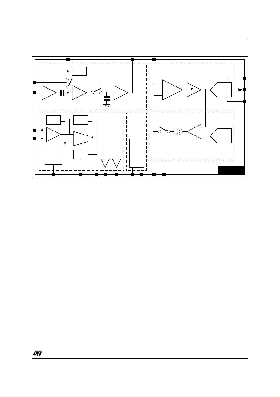
BLOCK DIAGRAM
STV0502
V
REF
G = 1 G = 1 G = 1
BIAS
G = 1
VREG
PSRR
BIAS
AGC
CORRELATED
DOUBLE
SAMPLING
AUDIO
INTERFACE
FUNCTIONAL DESCRIPTION
1 - Video Section
A CCD signal is provided to the STV0502, via a
coupling capacitor , as well as the pulses FS/FCDS.
The CDS (Correlated Double Sampling) is performing a clamp of the CCD signal during the FCDS
pulse. The signal obtained is then sampled during
the FS pulse, and held the rest of the period. The
resulting signal is then the difference between the
useful pixel level, and the pixel level corresponding
to no charge which can vary from one pixel to
another. Therefore, the parasitic level offset from
one pixel to another is removed.
This signal is DC coupled to the ACG, amplified by
a variable gain amplifier, bus controlled
(0.07dB step), which gain is in the range +6dB to
+23.7dB (17.7dB range). Typically, the amplifier is
controlled in order to keep the signal at an optimum
level (AGC) to be digitized. An extra 12dB can be
added up via a bit of the serial interface. In this cas e
the gain range becomes +18dB up to + 36dB.
At this point, the signal is clamped to a Black level
during the OB pulse. The black level is 5 bits bus
controlled, and its range corresponds to
[0 LSB ; 31 LSB] of the ADC. The black level is
made with a 5 bits DC frequency DAC, using the
same V
BOTTOM
and V
voltage references than
TOP
the ADC for matching purposes. The clamp is m ade
out of a OB puls e sampled comparator between the
VIDEO GAIN AMPLIFIER &
A/D CONVERTER INTERFACE
INTERFACE
SERIAL BUS
6dB/18dB
Range
0-18dB
COMP
ADJUST & CLAMP
A/D CONV
D/A CONV
BLACK LEVEL
STV0502
DAC output voltage (Black) and the ADC input
signal. The comparator has a symetrical current
output charging a capacitor. The obtained voltage
is buffered and used as a feedback to t he AGC
input stage. This clamp makes sure that ADCin is
matched to the DAC black settin g during the OB
pulse, disregarding any offset in the AGC path.
Then the signal is digitized by a fast ADC, clocked
at the pixel rate. The output of the chip is then an
8-bit pixel DATA, ready for digital post-processing.
2 - Audio Section
The chip integrates a high gain audio amplifier, in
order to process low signals coming from a speech
microphone, and provide on its output a line level,
differential audio signal, for digital conversion, or
power amplification. Two modes can be selected :
fixed gain mode or AGC mode. In case of AGC
mode, a peak detection of the signal is pe rformed
in order to regulate the output signal on a defined
level of 1.5V
level can be chosen at 1.5V
pin at respectively ground or supply voltage (a pullup resistor to supply is already included on chip),
for compatibility purposes between the 502 and
various back-end chips.
The system includes a Low-Noise fixed amplifier
(26dB), and a bias circuitry at the front.
or 1VPP (non-diff). This regulated
PP
or 1VPP thanks to a
PP
0502-02.EPS
3/15
Page 4

STV0502
FUNCTIONAL DESCRIPTION
(continued)
It is followed by a Voltage Controlled Amplifier
(range 8dB - 34dB), that can be switched into a
fixed 26dB gain amplifier.
The VCA output is differential and 2 buffers are
driving the two output pins, with a load impedance
down to 5kΩ.
A bias circuitry and an external capacitor (ACC)
form a DC feedback loop on the VCA DC bias, in
order to correct any DC offset on the VCA output.
Finally , a peak detector (double alternance) is used
to compare the output signal with the reference
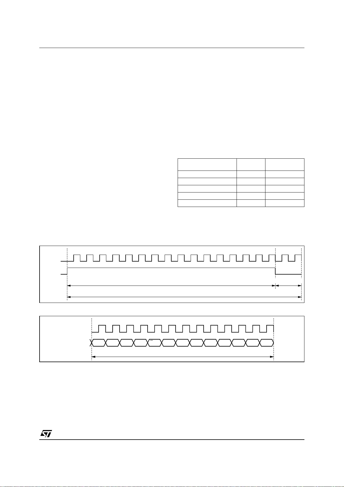
Figure 1
CDS_IN
FCDS
FS
CDS_OUT
ADC_IN
ADC_CLOCK
Pixel N
t1
t3
t2 t4
Sampling
Period
Pixel N+1 Pixel N+2 Pixel N+3 Pixel N+4 Pixel N+5
t
PROP
Pixel N Pixel N+1 Pixel N+2 Pixel N+3 Pixel N+4
t
DADC
threshold, to be regulated at. An external capacitor
(CAGC) is used for the AGC time constants. If the
signal goes above the threshold, a 500µA current
is charging the capacitor with a fast reponse
time(attack). In case of very big signals, a second
charge cureent of about 5mA is given, in order to
reduce the period during which the output signal is
saturated. Otherwise, a constant 1µA current discharges the capacitor with a slow response time
(decay). The capacitor voltage controls the VCA
gain. This constitues the AGC loop.
DATA_OUT
Notation :
Figure 2
4/15
Pixel N-4 Pixel N-3 Pixel N-2 Pixel N-1 Pixel N
3 CLK Pipe-Line Delay
- t1 is the delay between the falling edge of FCDS and the beginning of the active pixel level from the CCD.
- t2 is the delay between the falling edge of FS and the end of the active pixel level from the CCD.
t1, t2, t3 and t4 must be kept > 0 in the Application.
-t
is the propagation delay between CDS_OUT and ADC_IN signals (within the AGC block).
PROP
is the delay on the ADC outputs between the rising edge of the clock and data output.
-t
DADC
CDS_IN =
CCD Signal
FCDS
FS
CDS_OUT
Feedtrough Level
Signal Level
Pixel N+1
0502-03.EPS
0502-04.EPS
Page 5
STV0502
FUNCTIONAL DESCRIPTION
(continued)
3 - Serial Bus Specification
It is a 2-wires (data and clock) serial bus, used as
a slave.
Clock line is monodirectional (input) and allways
sent by the master to the chip, whereas Data line
is bidirectional (I/O).
There are 3 registers (8 bits), both writable/readable.
Each register can be addressed by a 4 bits address
word, followed by a R/W bit, and an 8 bits word Data
(read/write).
2 main patterns can be sent : Reset Pattern and
Read/Write pattern.
3.1 -Timings and Protocol
The data bit is t aken into ac count when t he clock
is rising.
- Reset Pattern : resets all the registers to their
default (Power On) values :
format = 16 * (data=1) | 2 * (data=0)
(total = 18 clocks)
- Read/Write Pattern :
format = 4 addr bits | R/W bit | 8 data bits
(total = 13 clocks)
Figure 3
Please note that :
1/ On power On conditions, SDATA line is in Write
(Input) Mode.
2/ In case of a read pattern, the SDATA line is
automatically set to Read (Output mode) during
8 clock cycles (Data D7 - D0) after R/W bit has
been sent, and comes back in Write (Input
mode) after the 13th clock cycle.
3/ There is no timing restriction between two
consecutive patterns (a pattern being defined
as one of the two above).
3.2 - Register Summary
Register
Video Amplifier Gain 0000 DDDD.DDDD
Black Level Adjust 0001 XXXD.DDDD
Video High Gain Select 0001 XXDX.XXXX
Test Mode 0001 DDXX.XXXX
Microphone AGC 0010 XXXX.XXXD
X : unused bits
D : means useful bits
Address
(A3-A0)
Data Format
(D7-D0)
Please note that 3 different functions are merged
in register address 01.
CLK
SDATA
Figure 4
1 2 3 4 5 6 7 8 9 10111213141516 1 2
2 CLK CyclesMinimum 16 CLK Cycles
Reset Pattern
12345678910111213
CLK
SDATA
A3 A2 A1 A0 R/W D7 D6 D5 D4 D3 D2 D1 D0
Read/Write Pattern
0502-05.EPS
0502-06.EPS
5/15
Page 6

STV0502
FUNCTIONAL DESCRIPTION
(continued)
3.3 - Control Data
Video Amplifier Gain Control
(8 bits used)
Address : 0000
POR value : 0000.0000 ---> 6dB
Gain is expressed from CDSoutput to ADC input
(ADC range 1.55V
PP
)
- 0.07dB / LSB step
- Overall range (256 steps) : 17.7dB
Video Gain (dB) Data
6 0000.0000
6.07 0000.0001
6.14 0000.0010
... ...
7.12 0001.0000
7.19 0001.0001
... ...
23.63 1111.1110
23.7 1111.1111
Black Level Adjustment Control
(5 bits used)
Address : 0001
POR Value : 0001.0000 ---> 16LSB
The adjustment is controlling the black reference
voltage. However, it is preferred to express the
Black level adjustment in terms of the ADC output
code variation (in ADC LSBs, compared to the
nominal default setting) depending on the Black
setting.
Typically, 16 LSBs black level is recommended.
- 1 ADC LSBs / LSB s tep
- Overall range : 31 ADC LSBs
Black Level
(ADC Ouput Variation)
0 LSBs XXX0.0000
1 LSBs XXX0.0001
... ...
30 LSBs XXX1.1110
31 LSBs XXX1.1111
Data
Video High Gain Select
(1 bit used)
Address : 0001
POR Value : 0 ---> Nominal gain
This bit controls an extra 12dB gain in the video
path (adding to gain described in previous page).
Video High Gain Select Data
Nominal Gain XX0X.XXXX
Extra 12dB Gain XX1X.XXXX
Video AGCOUT Test Signal ON/OFF
(2 bits use d)
Address : 0001
POR Value : 00 ---> High Z pad
A pin is reserved to output the ADC input signal, or
input the ADC input signal for t est and evaluation
purpose.
Those bits control the state of the output buffer. To
limit Xtalk and pollutions, the buffer is in High
impedance mode during normal operation.
VAGCOUT PIn State Data
Normal Operation (High Z Pin) 00XX.XXXX
AGC Output Test 10XX.XXXX
ADC Input Test 11XX.XXXX
Microphone AGC Switch
(1 bit used)
Address : 0010
POR value : 0000.0000 ---> AGC OFF
The switch is controlling the state of the AGC : ON
or OFF.
In OFF mode, the Micro Preamp. is set at a fixed
nominal gain of 52dB.
In ON mode, the AGC is operating in a gain range
[34dB ; 60dB] (see further in this document for
details).
Microphone AGC Data
OFF 0000.0000
ON 0000.0001
6/15
Page 7

STV0502
ABSOL UT E MAXIMUM RATIN G S
Symbol Parameter Value Unit
V
, V
DD
CC
V
I
I
I
T
stg
T
oper
T
lead
The STV0502 withstands 2kV in Human Body Model and 100V in Machine Model for all P ins versus
ESD :
V
and VSS.
DD
THERMAL DATA
Symbol Parameter Value Unit
R
th (j-a)
ELECTRICAL CHARACTERISTICS
T
= 25oC, VDD = VCC = 5V, unless otherwise specified
amb
Symbol Parameter Test Conditions Min. Typ. Max. Unit
SUPPLY
, VDDAll Supplies 4.5 5 5.5 V
V
CC
I
SUP
CMOS DIGITAL INPUTS
V
V
CMOS DIGITAL OUTPUTS (4mA drivers)
V
V
I
I
SERIAL INTERFACE
Slevel SDATA, SCLK Levels CMOS V
f
CLK
DutyC Clock Duty Cycle SCLK 40 50 60 %
t
t
Total Current Consumption VCC = VDD = 5V 40 55 70 mA
Low Level Input Voltage
IL
High Level Input Voltage 0.7 V
IH
Low Level Input Current
I
IL
I
High Level Input Current
IH
Low Level Output Voltage
OL
High Level Output Voltage 2.4
OH
Low Level Output Current
OL
High Level Output Current
OH
Bus Clock Frequency 0.5 1 MHz
Delay between CLK Rising Edge an d Data Out Read Mode, see Figure 5 300 500 700 ns
DR
Delay between CLK Rising Edge and Data In Write Mode, see Figure 5 300 500 700 ns
DW
Clock Rise Time SCLK 200 ns
t
R
t
Clock Fall Time SCLK 200 ns
F
Supply Voltage -0.5, 7 V
Digital Input Pin Voltage -0.5, VDD + 0.5 V
Digital Input Pin Current 1.6 mA
Storage Temperature +80
Operating Temperature 0, +70
Lead Temperature (10s Max.) +260
Junction-ambient Thermal Resistance Max. 65
DD
0.3 V
DD
-1.0
1.0
0.4 V
4.0
-4.0mAmA
o
o
C
o
C
o
C
C/W
V
V
µA
µA
V
0502-02.TBL
0502-03.TBL
0502-04.TBL
Figure 5
SCLK
SDATA_IO
t
R
t
F
t
DR
t
DW
0502-07.EPS
7/15
Page 8

STV0502
ELECTRICAL CHARACTERISTICS
T
= 25oC, VDD = VCC = 5V, unless otherwise specified (continued)
amb
Symbol Parameter Test Conditions Min. Typ. Max. Unit
VIDEO CDS
R
IN
C
IN
INDyn Input Dynamic Range Pin 4, before output clipping 0.6 0.7 V
CDS_SR S/H Slew Rate Pin 2, FS high 0.6 0.9 V/15ns
CDS_DR S/H Droop Rate Pin 2, FS low -20 +20 mV/µs
CDS_HM S/H Hold Mode Feed through Pin 2, FS low, f
CDS_lin CDS Linearity Pin 2, 500mV
CDS Gain Overall Input to Output Gain Pin 2, normal operation -2 -1 0 dB
R
OUT
OUTload CDS Ouput Load 100 Ω
FS PS Pulse Width See timings 12 ns
FCDS FSDS Pulse Width See timings 12 ns
PIX_FRE Pixel Rate Pins 4, 21, 22 6 12 MHz
PSRR Power Supply Rejection Measured on Pin 2 (2) 60 dB
VIDEO AMPLIFIER
R
IN
C
IN
Min. Gain
Max. Gain
Min. Gain
Max. Gain
Gset-err Gain Setting Relative Error Serial bus from H00 to HFF -0.5 0.5 dB
Out_Max Max. Output Signal before clipping Pin 38, V
t
R
t
F
t
PROP
PSRR Power Supply Rejection Measured on Pin 38 (2) 45 dB
Xtalk Xtalk from Video to Audio Measured on Pin 38, compared
Notes :
Input Resistance Pin 4 8 11 14 kΩ
Input Capacitance Pin 4 6 pF
= 1MHz -55 -45 dB
IN
(1) 0.3 1.5 %
PP
CDS Output Impedance Pin 2, FCDS & FS high 250 Ω
Input Resistance Pin 1 2 kΩ
Input Capacitance Serial bus from H00 to HFF 18 pF
Minimum Gain
Maximum Gain
Minimum Gain
Maximum Gain
Serial bus = H00/no extra gain
Serial bus = HFF/no extra gain 23.2623.7
Serial bus = H00/extra gain
Serial bus = HFF/extra gain 35.21235.7
= 4.5V
CC
G = 6dB, VIN = 0.8V
G = 23.7dB, VIN = 0.1V
PP
PP
1.6
1.6
6.5 dB
12.5 dB
Output Rise Time Square input 10 15 ns
Output Fall Time Square input 10 15 ns
AGC Propagation Time Pin 1 to Pin 38 15 20 ns
60 dB
to Pins 20 and 21 (2)
1. Normal operation means FS & FCDS run at specified timings and 12MHz frequency.
2. On a 20Hz to 10MHz frequenc y range, with 10µF filtering capacitors on all supplies, and well splitted supplies and grounds.
V
V
PP
dB
dB
PP
PP
0502-05.TBL
8/15
Page 9

STV0502
ELECTRICAL CHARACTERISTICS
T
= 25oC, VDD = VCC = 5V, unless otherwise specified (continued)
amb
Symbol Parameter Test Conditions Min. Typ. Max. Unit
8 BITS ADC & OB CLAMP
OB_rise OB High Time Constant Pin 38, OB 0 to 1 4 mV/µs
OB_decay OB Low Time Constant Pin 38, OB 1 to 0 -2 mV/ms
BLK_RAN Black Level Adjust Range Pins 8 to 15, OB high,
Serial bus from H00 to H1F
BLK_res Black Level Adjust Resolution Pins 8 to 15, per serial bus LSB step 1 LSBs
BLK_LEV Black Level Adjust Pins 8 to 15
Bus = H00
Bus = H1F 29031233
ADC_DN ADC Input Dynamic Range (output
from 0 to 255)
f
t
PCLK
t
DADC
R
V
V
CLK
LADD
TOP
BOT
ADC Clock Frequency Pin 24 12 MHz
Output Pipeline Delay (3) From a sampling to data out 3 3 CLK
Clock to Data Out (4) CLK positive edge, C
Ladder Resistance Between Pins 36 and 37 330 Ω
Top Reference Voltage Pin 36 3.2 3.35 3.5 V
Bottom Reference Voltage Pin 37 1.71 1.8 1.89 V
Pin 38 test signal above black
clamping level (V
BOT
)
= 20pF 17 ns
LOAD
ADC_lin ADC Linearity Data out, input signal between
Notes :
3. The signal is being sampled as long as ADC_CLK is high.
4. See Figure 6 for data reading timing constraint.
[V
BOT
+ 25mV ; V
TOP
- 25mV]
31 LSBs
LSBs
LSBs
1.4 1.55 1.7 V
cycles
1%
PP
0502-06.TBL
Figure 6
ADC_IN
ADC_CLOCK
DATA_OUT
Due to t
, and to make sure the data are read when they are stable, please read the data on the falling
DADC
edge of the ADC clock.
Sampling
Period
Pixel N-4 Pixel N-3 Pixel N-2 Pixel N-1 Pixel N
Pixel N
t
DADC
Pixel N+1
Data available
on falling edge of clock
0502-08.EPS
9/15
Page 10

STV0502
ELECTRICAL CHARACTERISTICS
T
= 25oC, VDD = VCC = 5V, unless otherwise specified (continued)
amb
Symbol Parameter Test Conditions Min. Typ. Max. Unit
MICROPHONE PREAMPLIFIER
V
BIAS
IN_ref Micro Input Voltage Pin 33 2 V
R
G
G
ALC1
ALC2
Ich AGC Charge Current On Pin 29 when signal out above threshold 500 µA
Idis AGC Discharge Current All the time with AGC on -1 µA
t
ATT
t
DEC
OUT_Max Output Clipping Level Pins 30/31
OUT_DC Output DC Voltage Pins 30/31 2.1 V
OUT_OF Channel DC Mismatch Pins 30/31 -350 0 350 mV
R
THD Overall THD 1V
PSRR PSRR from V
CMRR CMRR from V
LFc Low Cut-off Frequency C
HFc High Cut-off Frequency C
Xtalk Xtalk from video to audio Measure on Pins 30/31, compared to Pin 38 (2) 60 dB
Notes :
Bias Audio Voltage Pin 26 3.8 V
Input Impedance Pin 33 50 kΩ
IN
Overall Gain AGC Mode off 48 50 52 dB
FIX
Overall Gain AGC Mode on
AGC
Regulated Output Level On Pins 30/31, AGC on, Input = [1.5mV
Output Response Time Step +6dB, C
Output Response Time Step -6dB, C
Output Impedance Pins 30/31 100 Ω
OUT
CC
CC
2. On a 20Hz to 10MHz frequenc y range, with 10µF filtering capacitors on all supplies, and well splitted su ppl ie s and grounds.
V
= 0.5V
AGC
V
= 4V
AGC
; 30mVPP]
AGClevel (Pin 39) = 0
PP
AGClevel (Pin 39) = 5
= 2.2µF5ms
AGC
= 2.2µF 2.5 s
AGC
AGC off : V
AGC on : VIN > 40mV
out, 1kHz signal, BW 15kHz 0.15 0.4 %
PP
= 5mV
IN
PP
PP
54 56205834dB
1.1
1.511.9
0.7
1.3
1.7
1.722
f = 1kHz, VCC + sine 100mVPP (2) 60 dB
f = 1kHz, VCC + sine 100mVPP (2) 60 dB
= 2.2µF, C
IN
= 2.2µF, C
IN
= 10µF 250 Hz
ACC
= 10µF 20 kHz
ACC
V
V
V
V
dB
PP
PP
PP
PP
0502-07.TBL
Figure 7
10/15
INPUT
OUTPUT
+6dB -6dB
t
t
ATT
DEC
0502-09.EPS
Page 11

I/O DIAGRAMS
Figure 8 :
VAGCIN
VAGCIN
STV0502
Figure 9 :
1.33k
W
1
W
8.67k
CDS_OUT
2
CDS_OUT
Figure 10 :
Figure 12 :
Figure 14 :
CDS_REF
3
CDS_REF
DATA[7:0]
DATA[7:0]
Pins 8 to 15
OB, FCDS, FS, SCLK, ADC_CLOCK
0502-10.EPS
Figure 11 :
0502-12.EPS
Figure 13 :
SDATA_IO
0502-14.EPS
Figure 15 :
CDS_IN
220
CDS_IN
4
SDATA_IO
18
W
MICRO_IN
10k
0502-11.EPS
W
0502-13.EPS
0502-15.EPS
OB, FCDS, FS
SCLK, ADC_CLOCK
Pins 20, 21, 22, 23, 24
220
W
MICRO_IN
0502-16.EPS
26
0502-17.EPS
11/15
Page 12

STV0502
I/O DIAGRAMS
Figure 16 :
Figure 18 :
MIC_REF
CAGC
(continued)
27
MIC_REF
29
CAGC
Figure 17 :
0502-18.EPS
Figure 19 :
ACC
28
AF_OUT+, AF_OUT -
10k
W
10k
W
ACC
0502-19.EPS
AF_OUT+,
AF_OUTPins 30/31
Figure 20 :
Figure 22 :
40k
V
V
BIAS
BOT
W
330
22k
0502-20.EPS
Figure 21 :
33
V
BIAS
W
0502-22 .EPS
Figure 23 :
W
10k
W
37
V
BOT
0502-24.EPS
V
TOP
10k
W
VAGCOUT
330
38
VAGCOUT
36
V
TOP
W
0502-21.EPS
0502-23.EPS
0502-25.EPS
12/15
Page 13

STV0502
I/O DIAGRAMS
Figure 24 :
AGCLEVEL
Figure 26 :
AGCLEVEL
39
BLACK_REF
(continued)
42
BLACK_REF
Figure 25 :
0502-26.EPS
0502-28.EPS
OB_CAP
40
OB_CAP
0502-27.EPS
13/15
Page 14

STV0502
TYPICAL APPLICATION
From
CCD
DATA[7]
DATA[6]
DATA[5]
DATA[4]
DATA[3]
DATA[2]
DATA[1]
DATA[0]
33nF
1
F
m
FCDS
V
ADC
3435
GND
MICRO_REF
MICRO_IN
ADC_CLOCK
FCDS
FS
DD
10mF
CC
V
V
AF_OUT-
AF_OUT+
CAGC
ACC
GND
SCLK
FS
10mF
V
33
BIAS
V
32
CC
31
30
6.8mF
29
28
27
5.1k
26
25
24
CC
Micro
10mF
LINE
OUTPUTS
3.3k
W
10mF
10mF
W
2.2mF
3 x 1N4148
1k
W
MICROPHONE
ADC_CLOCK
23
SCLK
SERIAL
INTERFACE
SDATA
0502-29.EPS
V
CC
Video
10mF
CC
V
GND
VAGCIN
1
CDS_OUT
2
1
m
F
CDS_REF
3
CDS_IN
4
GND
5
NC
6
NC
7
DATA[7]
8
DATA[6]
9
DATA[5]
10
DATA[4]
11
DATA[3]
DATA[2]
BLACK_REF
DATA[1]
12 13 14 15 21 22
220nF
OB_CAP
39
AGCLEVEL
41424344
NC
STV0502
VDDVDDSDATA_IO
DATA[0]
16 17 18 19 20
V
DD
1mF1mF
36373840
TOP
BOT
V
V
TESTONLY
OB
GND
OB
OB
14/15
Page 15

PACKAGE MECHANICAL DATA
44 PINS - FULL PLASTIC QUAD FLAT PACK (THIN) (TQFP)
44 34
1
e
33
E3
E1
0,10 mm
.004 inch
SEATING PLANE
E
STV0502
A
A2
A1
B
23
c
L1
L
0,25 mm
.010 inch
K
GAGE PLANE
Dimensions
11
12 22
D3
D1
D
Millimeters Inches
Min. Typ. Max. Min. Typ. Max.
A 1.60 0.063
A1 0.05 0.15 0.002 0.006
A2 1.35 1.40 1.45 0.053 0.055 0.057
B 0.30 0.37 0.40 0.012 0.015 0.016
C 0.09 0.20 0.004 0.008
D 12.00 0.472
D1 10.00 0.394
D3 8.00 0.315
e 0.80 0.031
E 12.00 0.472
E1 10.00 0.394
E3 8.00 0.315
L 0.45 0.60 0.75 0.018 0.024 0.030
L1 1.00 0.039
K0
Information furnished is believed to be accurate and reliable. However, STMicroelectronics assumes no responsibility for the
consequences of use of such information nor for any infringement of patents or other rights of third parties which may result from
its use. No licence is granted by implication or otherwise under any patent or patent rights of STMicroelectronics. Specifications
mentioned in this publication are subject to change without notice. This publication supersedes and replaces all information
previously supplied. STMicroelectronics products are not authorized for use as critical components in life support devices or sys tem s
without express written approv al of STMi cr oelec troni cs.
Purchase of I
Rights to use these components in a I
Australia - Brazil - Canada - China - France - Germany - Italy - Japan - Korea - Malaysia - Malta - Mexico - Morocco - The Neth erlands
Singapore - Spain - Sweden - Switzerland - Taiwan - Thailand - United Kingdom - U.S.A.
The ST logo is a registered trademark of STMicroelectronics
© 1998 STMicroelectronics - All Rights Reserved
2
C Components of STMicroelectronics, conveys a license under the Philips I2C Pate n t .
2
the I
C Standard Specifications as defined by Phili ps.
2
C system, is granted provided that the system conforms to
STMicroelectronics GROUP OF COMPANIES
http://www.st.com
o
(Min.), 7o (Max.)
15/15
PM-4Y.EPS
4Y.TBL
 Loading...