

Page 1
■
MULTISTANDARD QPSK AND BPSK
DEMODULATION
■
EASY IMPLEMENTATION WITH LOW COST
DIRECT CONVERSION TUNERS
■
EXTREMELY LOW BER WHEN
CO-CHANNEL INTERFERENCE
■
WIDE CARRIER LOOP TRACKING RANGE TO
COMPENSATE FOR DISH FREQUENCY DRIFT
■
COMMON INTERFACE COMPLIANT
■
VERY LOW POWER CONSUMPTION
■
INTEGRATED DUAL 6-BIT ANALOG TO
DIGITAL CONVERTERS
■
DUAL DIGITAL AGC
■
DIGITAL NYQUIST ROOT FILTER WITH
ROLL-OFF OF 0.35 OR 0.20
■
DIGITAL CARRIER LOOP WITH LOCK
DETECTOR, ON-CHIP WIDE RANGE
DEROTATOR AND TRACKING LOOP
(TYP ± 45 MHz)
■
DIGITAL TIMING RECOVERY WITH LOCK
DETECTOR
■
CHANNEL BIT RATE UP TO 90 Mbps AND
SYMBOL FREQUENCY RATE FROM
1 TO 50 MSYMBOLS
■
INNER DECODER:
- VITERBI SOFT DECODER FOR
CONVOLUTIONAL CODES, M=7, RATE 1/2
- PUNCTURED CODES 1/2, 2/3, 3/ 4, 5/6, 6/7 AND 7/8
■
SYNCHROWORD EXTRACTION
■
CONVOLUTIVE DEINTERLEAVER
■
OUTER DECODER:
- REED-SOLOMON DECODER FOR
16 PARITY BYTES; CORRECTION OF UP
TO 8 BYTE ERRORS
- ENERGY DISPERSAL DESCRAMBLER
■
ON-CHIP FLEXIBLE CLOCK SYSTEMS TO
ALLOW USE OF EXTERNAL CLOCK
SIGNALS IN 4 MHz TO 30 MHz RANGE
■
EASY-TO-USE C/N ESTIMATOR WITH 2 TO
18 dB RANGE
■
I2C SERIAL BUS AND REPEATER
■
DVB COMMON INTERFACE COMPLIANT
PARALLEL OUTPUT FORMAT
■
PARALLEL AND SERIAL DATA OUTPUT
■
LNB SU PPLY CO NTROL WITH STANDARD I/O,
22 KHz TONE AND DISEQC
TM
MODULATOR
WITH TTL OUTPUT
■
CMOS TECHNOLOGY: 2.5 V OPERATION;
JEDEC (EIA/JESD8-5)
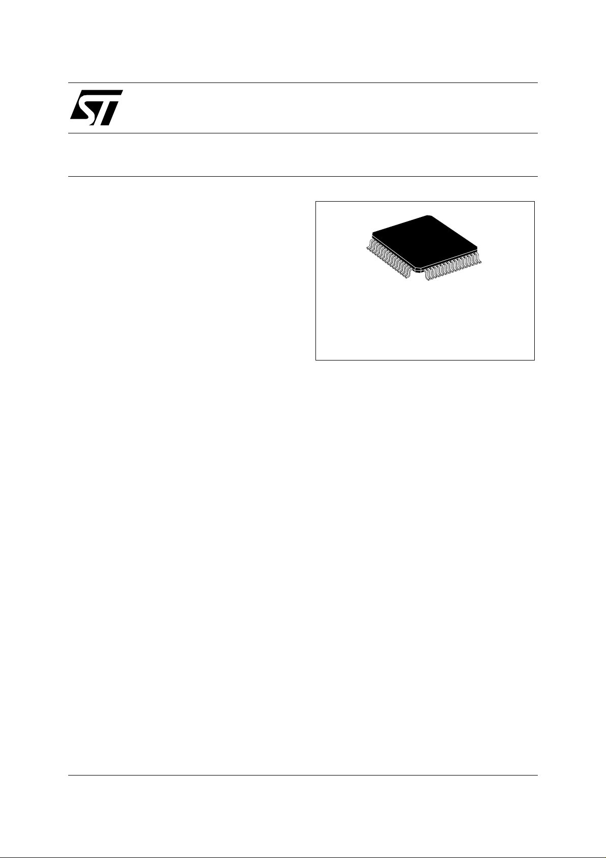
STV0299B
QPSK/BPSK LINK IC
TQFP64
(Thin Plastic Quad Flat Pack)
ORDER CODE:
APPLICATIONS
■
DIGITAL SATELLITE RECEIVER AND
SET-TOP BOXES
DESCRIPTION
The STV0299 Satellite Receiver with FEC is a
CMOS single-chip multistand ard demodulator for
digital satellite broadcasting. It consists of two A/D
converters for I-input and Q-input, a multistandard
QPSK and BPSK demodulator, and a forward
error correction (FEC) unit having both a n inner
(Viterbi) and outer (Reed-Solomon) decoder.
The FEC unit is compliant with the DVB-S and
TM
specifications. Processing is fully digital.
DSS
It integrates a derotator before the Nyquist root
filter, allowing a wide range of offset tracking.
The high sampling rate facilitates the
implementation of low-cost, direct conversion
tuners.
A variety of configurations and beh aviours can be
selected through a bank of control/configuration
registers via an I
Transport Streams and interfaces seamlessly to
the Packet Demultiplexers embedded in ST’s
ST20-TPx or STi55xx. High sampling frequency
(up to 90MHz) considerably reduces the cost of
LPF of direct conversion tuners.
The multistandard capability associated with a
broad range of input frequency operat ions makes
it easy-to-use. Its low power consumption, small
package and optional serial output interface
makes it perfect for embedding into a tuner.
(10 x 10 x 1.4 mm)
STV0299B (
2
C. The chip outputs MPEG
No Slug)
May 2000 1/36
This is preliminary information on a new product now in development or undergoing evaluation. Details are subject to change without not i ce.
Page 2

STV0299B
PageTABLE OF CONTENTS
1 PIN INFORMATION . . . . . . . . . . . . . . . . . . . . . . . . . . . . . . . . . . . . . . . . . . . . . . . . . . . . . . . . . . . . . . 4
1.1 Pin Connections . . . . . . . . . . . . . . . . . . . . . . . . . . . . . . . . . . . . . . . . . . . . . . . . . . . . . . . . . . . 4
1.2 Pinout Description. . . . . . . . . . . . . . . . . . . . . . . . . . . . . . . . . . . . . . . . . . . . . . . . . . . . . . . . . . 5
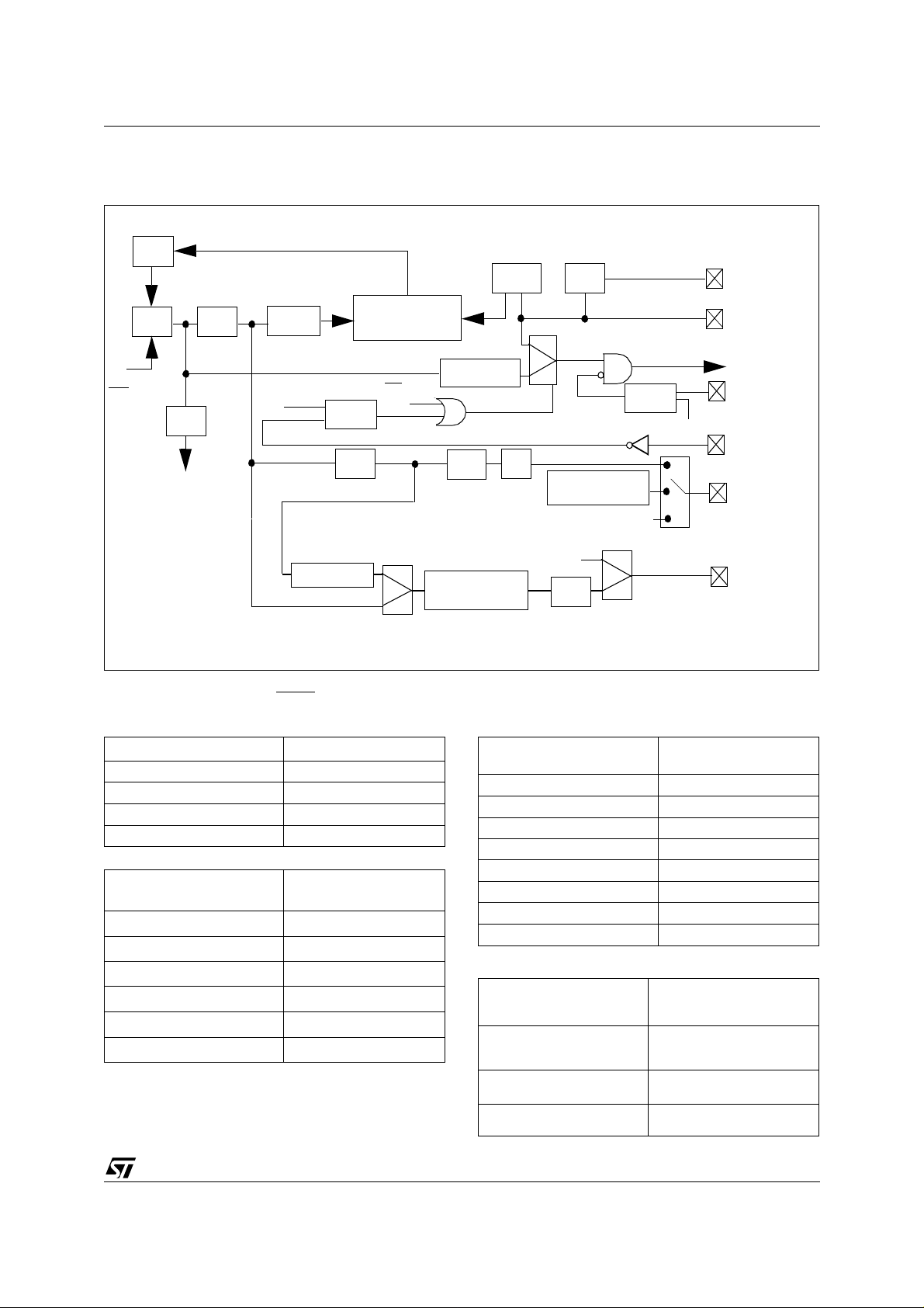
2 BLOCK DIAGRAM. . . . . . . . . . . . . . . . . . . . . . . . . . . . . . . . . . . . . . . . . . . . . . . . . . . . . . . . . . . . . . . 6
3 SYSTEM CHARACTERISTICS . . . . . . . . . . . . . . . . . . . . . . . . . . . . . . . . . . . . . . . . . . . . . . . . . . . . . 6
4 FUNCTIONAL DESCRIPTION . . . . . . . . . . . . . . . . . . . . . . . . . . . . . . . . . . . . . . . . . . . . . . . . . . . . . . 7
4.1 Front End Interfaces . . . . . . . . . . . . . . . . . . . . . . . . . . . . . . . . . . . . . . . . . . . . . . . . . . . . . . . . 7
4.2 Signal Processing . . . . . . . . . . . . . . . . . . . . . . . . . . . . . . . . . . . . . . . . . . . . . . . . . . . . . . . . . 12
4.3 Timing Recovery . . . . . . . . . . . . . . . . . . . . . . . . . . . . . . . . . . . . . . . . . . . . . . . . . . . . . . . . . . 13
4.4 Carrier Recovery and Derotator Loop . . . . . . . . . . . . . . . . . . . . . . . . . . . . . . . . . . . . . . . . . 14
4.5 Noise Indicator. . . . . . . . . . . . . . . . . . . . . . . . . . . . . . . . . . . . . . . . . . . . . . . . . . . . . . . . . . . . 14
4.6 Forward Error Correction . . . . . . . . . . . . . . . . . . . . . . . . . . . . . . . . . . . . . . . . . . . . . . . . . . . 15
5 REGISTER LIST. . . . . . . . . . . . . . . . . . . . . . . . . . . . . . . . . . . . . . . . . . . . . . . . . . . . . . . . . . . . . . . . 19
6 ELECTRICAL CHARACTERISTICS . . . . . . . . . . . . . . . . . . . . . . . . . . . . . . . . . . . . . . . . . . . . . . . . 29
6.1 Absolute Maximum Ratings . . . . . . . . . . . . . . . . . . . . . . . . . . . . . . . . . . . . . . . . . . . . . . . . . 29
2
4.1.1 I
C Interface. . . . . . . . . . . . . . . . . . . . . . . . . . . . . . . . . . . . . . . . . . . . . . . . . . . . . . . . . . . 7
4.1.2 Write Operation (Normal Mode). . . . . . . . . . . . . . . . . . . . . . . . . . . . . . . . . . . . . . . . . . . . 7
4.1.3 Read Operation (Normal Mo de). . . . . . . . . . . . . . . . . . . . . . . . . . . . . . . . . . . . . . . . . . . . 7
2
4.1.4 I
C Interface in Standby Mode . . . . . . . . . . . . . . . . . . . . . . . . . . . . . . . . . . . . . . . . . . . . . 7
4.1.5 Specific Concerns about SCL Freq uency . . . . . . . . . . . . . . . . . . . . . . . . . . . . . . . . . . . . 8
4.1.6 Identification Register. . . . . . . . . . . . . . . . . . . . . . . . . . . . . . . . . . . . . . . . . . . . . . . . . . . . 8
4.1.7 Sampling Freque nc y . . . . . . . . . . . . . . . . . . . . . . . . . . . . . . . . . . . . . . . . . . . . . . . . . . . . 8
4.1.8 Clock Generation . . . . . . . . . . . . . . . . . . . . . . . . . . . . . . . . . . . . . . . . . . . . . . . . . . . . . . . 8
4.1.9 Clock Registers . . . . . . . . . . . . . . . . . . . . . . . . . . . . . . . . . . . . . . . . . . . . . . . . . . . . . . . 1 0
4.1.10 I2C Bus Repeater . . . . . . . . . . . . . . . . . . . . . . . . . . . . . . . . . . . . . . . . . . . . . . . . . . . . . 10
4.1.11 General Purpose Σ∆DAC . . . . . . . . . . . . . . . . . . . . . . . . . . . . . . . . . . . . . . . . . . . . . . 10
4.1.12 DiSEqC Interface . . . . . . . . . . . . . . . . . . . . . . . . . . . . . . . . . . . . . . . . . . . . . . . . . . . . . 10
4.1.13 Standby Mode . . . . . . . . . . . . . . . . . . . . . . . . . . . . . . . . . . . . . . . . . . . . . . . . . . . . . . . 11
4.2.1 I and Q Inputs. . . . . . . . . . . . . . . . . . . . . . . . . . . . . . . . . . . . . . . . . . . . . . . . . . . . . . . . . 1 2
4.2.2 Main AGC (or AGC1). . . . . . . . . . . . . . . . . . . . . . . . . . . . . . . . . . . . . . . . . . . . . . . . . . . 12
4.2.3 Nyquist Root and Interpolation Filters . . . . . . . . . . . . . . . . . . . . . . . . . . . . . . . . . . . . . . 12
4.2.4 Offset Cancellation. . . . . . . . . . . . . . . . . . . . . . . . . . . . . . . . . . . . . . . . . . . . . . . . . . . . . 12
4.2.5 Signal AGC (or AGC2). . . . . . . . . . . . . . . . . . . . . . . . . . . . . . . . . . . . . . . . . . . . . . . . . . 12
4.3.1 Timing Control . . . . . . . . . . . . . . . . . . . . . . . . . . . . . . . . . . . . . . . . . . . . . . . . . . . . . . . . 13
4.3.2 Loop Equation . . . . . . . . . . . . . . . . . . . . . . . . . . . . . . . . . . . . . . . . . . . . . . . . . . . . . . . . 13
4.3.3 Timing Lock Indicator. . . . . . . . . . . . . . . . . . . . . . . . . . . . . . . . . . . . . . . . . . . . . . . . . . . 13
4.4.1 Loop Parameters . . . . . . . . . . . . . . . . . . . . . . . . . . . . . . . . . . . . . . . . . . . . . . . . . . . . . . 1 4
4.4.2 Carrier Lock Detector. . . . . . . . . . . . . . . . . . . . . . . . . . . . . . . . . . . . . . . . . . . . . . . . . . . 14
4.4.3 Derotator Frequency . . . . . . . . . . . . . . . . . . . . . . . . . . . . . . . . . . . . . . . . . . . . . . . . . . . 14
4.4.4 Carrier Frequency Offset Detector. . . . . . . . . . . . . . . . . . . . . . . . . . . . . . . . . . . . . . . . . 14
4.6.1 FEC Modes . . . . . . . . . . . . . . . . . . . . . . . . . . . . . . . . . . . . . . . . . . . . . . . . . . . . . . . . . . 15
4.6.2 Viterbi Decoder and Synchronization. . . . . . . . . . . . . . . . . . . . . . . . . . . . . . . . . . . . . . . 15
4.6.3 Synchronization . . . . . . . . . . . . . . . . . . . . . . . . . . . . . . . . . . . . . . . . . . . . . . . . . . . . . . . 16
4.6.4 Error Monitoring . . . . . . . . . . . . . . . . . . . . . . . . . . . . . . . . . . . . . . . . . . . . . . . . . . . . . . . 16
4.6.5 Convolutional Deinterleaver. . . . . . . . . . . . . . . . . . . . . . . . . . . . . . . . . . . . . . . . . . . . . . 16
4.6.6 Reed-Solomon Dec oder and Desc ramb ler . . . . . . . . . . . . . . . . . . . . . . . . . . . . . . . . . . 16
4.6.7 Parallel Output Interface . . . . . . . . . . . . . . . . . . . . . . . . . . . . . . . . . . . . . . . . . . . . . . . . 16
4.6.8 Serial Output Interface. . . . . . . . . . . . . . . . . . . . . . . . . . . . . . . . . . . . . . . . . . . . . . . . . . 17
2/36
Page 3

STV0299B
(continued)
PageTABL E OF CONTENTS
6.2 Thermal Data . . . . . . . . . . . . . . . . . . . . . . . . . . . . . . . . . . . . . . . . . . . . . . . . . . . . . . . . . . . . . 29
6.3 DC Electrical Characteristics. . . . . . . . . . . . . . . . . . . . . . . . . . . . . . . . . . . . . . . . . . . . . . . . 29
6.4 Timing Characteristics . . . . . . . . . . . . . . . . . . . . . . . . . . . . . . . . . . . . . . . . . . . . . . . . . . . . . 31
2
C Bus Characteristics. . . . . . . . . . . . . . . . . . . . . . . . . . . . . . . . . . . . . . . . . . . . . . . . . . . . . 32
6.5 I
7 APPLICATION BLOCK DIAGRAMS. . . . . . . . . . . . . . . . . . . . . . . . . . . . . . . . . . . . . . . . . . . . . . . . 33
8 PACKAGE MECHANICAL DATA . . . . . . . . . . . . . . . . . . . . . . . . . . . . . . . . . . . . . . . . . . . . . . . . . . 35
3/36
Page 4
STV0299B
1 PIN INFORMATION
1.1 Pin Connections
Figure 1:
Pinout for 64-pin TQFP (10x10 mm)
CLK_IN/XTAL_IN
XTAL_OUT
V
AUX_CLK
V
DD_3.3V
RESET
F22/DiSEqC
V
SSA
DDA
V
SS
V
DD
V
SS
AGC
V
DD
V
SS
SDA
SCL
SS
DD
V
V
64 62 61 60 59 58 57 56 5563 54 53 52 51 50 49
1
2
3
4
5
6
7
8
9
10
11
12
13
14
15
16
17 19 20 21 22 23 24 25 2618 27 28 29 30 31 32
TEST
TEST
SDAT
SCLT
SSA
V
DIRCLK-DIS
DDA
TOP
V
QP
V
QN
SSA
V
IN
IP
SSA
V
V
48
47
46
45
44
43
42
40
39
38
37
36
35
34
33
41
BOT
V
DDA
TEST
TEST
TEST
TEST
STDBY
V
DD
DAC
V
SS
IP0
TEST
D0
D1
D2
D3
4/36
V
SS
D6
D5
V
DD
STR_OUT
SS
V
DD_3.3 V
V
CLK_OUT
OP1
OP0
D/P
ERROR
LOCK/OP2
D4
SS
V
SERIAL DATA/D7
Page 5
STV0299B
1 PIN INFORMATION
(continued)
1.2 Pinout Description
Pin Number Name
SIGNAL INPUTS
50, 51 IP, IN I Analog in Phase Component
53, 54 QN, QP I Analog in Quadrature Component
1 CLK_IN/XTAL IN I Crystal Input or CLK_IN
2 XTAL OUT O Crystal Output
9AGC
5 AUX_CLK
17-18 OP0, OP1
19 LOCK/OP2
38 IP0 I Input Port
SIGNAL OUPUTS
26-28-29-31, 33 to 36 D[7:0]
24 CLK_OUT
22 STR_OUT
21 D/P
20 ERROR
14 SCL
12 SDA
OTHERS
59 SCLT
60 SDAT
37-43-44-45-46-61-62 TEST I
58 DIRCLK_DIS I
3, 49, 52, 57
4, 47, 55
56
48
6-8-11-23-27-32-39-64
13-25
7-10-30-41-63
15 RESET
42 STDBY I Sets STDBY at power on
16 F22/DiSEqC
40 DAC
Note: 1
The following abbreviations are used: I - Input; O - Output; OD - Open drain output.
2
3.3 V outpu t levels.
3
5 V tolerant
V
SSA
V
DDA
V
TOP
V
BOT
V
SS
V
DD_3.3 V
V
DD
1
I/O
FRONT END CONTROLS
3
Control Signal to the Tuner
OD
2
Programmable Output Port or Programmable Output Clock
O
2
Programmable Output Ports
O
2
Carrier Found or Data Found or Output Port
O
2
Output Data; D7 is DATA_OUT in Serial Mode
O
2
Output Byte Clock; or Bit Clock in Serial Mode
O
2
Output 1st byte Signal (synchro byte clock)
O
2
Data/Parity Signal
O
2
Output Error Signal. Set in case of uncorrectible packet.
O
I2C INTERFACE
3
Serial Clock (I2C bus)
I
3
I/OD
Serial Data (I2C bus)
3
Tuner Serial Clock (repeator) or Output Port
OD
3
Tuner Serial Data (repeator) or Input/Output Port
I/OD
Reserved for manufacturing tests; must be tied to V
Sets the DIRCLK function at power on
S Analog Ground
S Analog 2.5 V Supply
S ADC High Voltage Reference
S ADC Low Voltage Reference
S Ground
S 3.3 V Supply
S 2.5 V Supply
I Reset, active at low level
DiSEqC modulation, 22 kHz Tone, Programmable
2
O
Output Port
2
Programmable Digital to Analog Converter Output
O
Description
SS
5/36
Page 6

STV0299B
-
2 BLOCK DIAGRAM
AGC
V
DDA
V
TOP
IN/IP
QN/QP
V
BOT
V
SSA
CLK_IN/XTAL_IN
AUX_CLK
Nyquist &
Interpolation
Filter
Derotator
AGC1
Offset
Comp.
ADCs
Clock
Generator
AGC2
Carrier Lock
Indicator
Error
Monitoring
Timing
Recovery
Timing
DCO
Timing
Lock
Indicator
C/N
Indicator
Viterbi Decoder
Deinterleaver
XTAL_OUT
F22/DiSEqC
SCL
SDA
22 kHz
Tone
DiSEqC
Interface
2
I
C
Interface
SDAT SCLT DAC IP0 OP0[2:0] D[7:0] V
General
Purpose
Functions
3 SYSTEM CHARACTERIST ICS
Performances
The following given parameters are for indication
purposes only.
Carrier Loop Tracking Range:
M_CLK
/2
• ±f
Carr i er Loop Ca pt ure Range ( C / N>=4 dB):
• up to ± 5% fs in less than 100 Ksymbols
• up to ± 2% fs in less than 10 Ksymbols
C/N Threshold (lowest C/N at which capture is
possible) = 1 dB.
Reed-Solomon
Decoder
D/P
Energy
Descrambler
DD_3.3VVDDVSS
ERROR
STR_OUT
CLK_OUT
Timi ng Loop Capt ure Range (C/N>=2 dB ):
• up to ±250 ppm in less than 100 Ksymbols
• conventions used for the above characteristics
are:
f
sampling
fs = f
C/N = Carrier/Noise =
PR = Puncture Rate
= f
symbol
m_clk
= f
master_clock
Eb
------ -x2xPR
No
6/36
Page 7
4 FUNCTIONAL DESCRIPTION
STV0299B
The STV0299B is a multistandard demodulator
and error correction decoder IC for the reception
of QPSK and BPSK modulated signals. It is
intended for use in digital satellite television
applications. The IC can accept two standards of
QPSK modulated signals (DVB and DSS) as well
as BPSK modulated signals over a wide symb ol
frequency range (from 1 to 50 Msymbol s/s). The
signals are digitized via an integrated dual 6-bit
analog to digital converter, and interpolated and
digitally filtered by a Nyquist root filter (with a
settable roll-off value of either 0.35 or 0.20).
There are two built-in digital Automatic Gain
Controls (AGCs). The first AGC allows the tuner
gain to be controlled by the pulse density
modulated output. The second AGC performs
power optimization of the digital signa l bandwidth
(internal to the STV0299B). The digital signal then
passes through the digital carrier loop fitted with
an on-chip derotator and tracking loop, lock
detector, and digital timing recovery.
Forward error correction is integrated by way of an
4.1.2 Write Operation (Normal Mode)
The byte sequence is as follows:
1 The first byte gives the device address plus the
direction bit (R/W = 0).
2 The second byte contains the internal address
of the first register to be accessed.
3 The next byte is written in the internal regist er.
Following bytes (if any) are written in
successive internal registers.
4 The transfer lasts until stop conditions are
encountered.
5 The STV0299B acknowledges every byte
transfer.
4.1.3 Rea d Op e rat i on (N ormal Mode )
The address of the first register to read is
programmed in a write operation without data, and
terminated by the stop condition. Then, another
start is followed by the device address and R/
W = 1. All following bytes are now data to be read
at successive positions starting from the initial
address. Figure 2 shows the I
2
C Normal Mode
Write and Read Registers.
inner Viterbi soft decoder, and an outer
Reed-Solomon decoder.
4.1 Front End Interfaces
2
4.1.1 I
The standard I
first byte is Hex D0 fo r a write operation, or Hex
D1 for a read operation. The I
C Interface
2
C protocol is used whereby the
2
C interface
operates differently depending on whether it is in
normal or standby mode.
4.1.4 I
Only three registers can be addressed while in
standby mode: RCR (address 01 Hex), MCR
(address 02 Hex) and ACR (address 03 Hex).
These three registers can be either read or written
to (refer to Figure 3).
Only one register may be read or written to per
sequence (no increment). While in standby mode,
the Serial Clock (SCL) frequency must be lower than
one tenth of the CLK_IN frequency (f
Figure 2:
Write registers 0 to 3 with AA, BB, CC, DD
Start
Read registers 2 and 3
Start Device Address, Write D 0 ACK Register Address 02 ACK Stop
Start
Figure 3:
Write operation
Star t Device A ddress, Wri te D0 ACK Register Address 01, 02 or 03 ACK Data ACK Stop
2
I
C Read and Write Operations in Normal Mode
Device
Address,
Write D0
2
I
C Read and Write Operations in Standby Mode
ACK
Device Address,
Read D1
Register
Address 00ACK
ACK Data Read CC ACK Data Read DD
Data
AA
ACK
2
C Interface in Standby Mode
Data
BB
ACK
Data
CC
ACK
Data
DD
CLK_IN
/ 10).
ACK Stop
ACK
Stop
Read operation
Start
Start
Note: 1
ACK is not absolutely necessary after Data
Device Address
, Read D0
Device Ad dress,
Read D1
ACK Regis ter Address ACK Stop
ACK Reader Data
ACK (or no
ACK
Stop
1
)
7/36
Page 8

STV0299B
N
4 FUNCTIONAL DESCRIPTION
(continued)
4.1.5 Specific Concerns about SCL
Frequency
For reliable operation in Normal Mode, the SCL
frequency must be lower than 1/40 of the Ma ster
Clock (M_CLK) frequency. Consequently, care
should be taken to observe the following:
1 Before returning t o No rm al Mode from Sta ndby
Mode, the M_CLK frequency must be s elected
≥
such that f
M_CLK
40 f
SCL
2 After Power-on reset signal, the STV0299B
operates in Normal Mode. There are two possible cases:
- DIRCLK-DIS (pin 58) is grounded.
M_CLK = CLK_IN, the f
2
I
C bus must satisfy:
- DIRCLK-DIS (pin 58) is tied to V
100
(where ), and the f
f
M_CLK
--------- -
=
16
frequency of the
SCL
CLK_IN
f
≤
-------------------- -
SCL
f
⋅
CLK_I
40
.
DD
SCL
frequency of the I2C bus must satisfy:
f
SCL
16 40
CLK_IN
⋅≤
×
and
f
SCL
≤
400 kHz.
100
-------------------
For example, this second operating mode is
required when the app lication features both a
4 MHz XT AL and a 400 kHz I
2
C bus.
4.1.6 Identification Register
The Identification Register (at address Hex 00)
gives the release number of the circuit.
The content of this register at reset is presently A1
(same as STV0299).
4.1.7 Sampl i ng Frequency
The STV0299B converts the analog inputs into
digital 6-bit I and Q flows. The sampling frequency
is f
reference described in Section 4.1.8
Generation’
which is derived from an external
M_CLK
. The maximum value of f
‘Clock
M_CLK
is 90
MHz.
The sampling causes the repetition of the input
spectrum at each integer multiple of f
M_CLK
. One
has to ensure that no frequency component is
folded in the useful signal b andwidth of f
where f
is the symbol frequency, and α is the
S
(1+α)/2
S
roll-off value.
4.1.8 Clock Generation
An integrated VCO (optimised to r un in the range
of 300 to 400 MHz) is locked to a reference
frequency provided by a crystal o scillator by the
following relation:
M1
+
f
VCOfref
4M1
==
()⋅⋅
f
+
XTAL
4
⋅⋅
--------------
K1
+
The VCO’s loop filter is optimized for a reference
frequency between 4 and 8 MHz.
The VCO generates the following by division:
• The Master Clock (M_CLK)
• An auxiliary clock (AUX_CLK) which may either
be in the MHz range or in the 25 Hz to 1500 Hz
range for some specific LNB control (for
example, 60 Hz).
• A lower frequency, F22, typically 22 KHz,
needed for LNB control or DiSEqC
TM
control.
When DIRCLK_CTRL = 1, the crystal signal is
routed directly to M_CLK; the VCO may still be
used to generate AUX_CK and/or the F22 (used
by the DiSEqC
TM
int erface).
If the internal VCO is not used by any of the
dividers, it may be stopped in order to decrease
the power consumption and/or radiation
emissions. The only guaranteed function in
standby mode is the I
2
C Write/Read function of
the three clock control registers.
There are restrictions on the high and low level
durations, and on the crystal (or external clock)
frequency when the direct clock is used.
These restrictions are explained in Section 4.1.5
Specific Concerns about SCL Frequency
.
8/36
Page 9
STV0299B
)
]
]
]
]
g
4 FUNCTIONAL DESCRIPTION
Figure 4:
Clock Signal Generation
LPF
Reg 01[4:0
VCO 1/4
VCO
/OFF
ON
TO SERIAL
SHIFTER
1/6
÷(M+1)
I2C
Note 2
PRESCALER
(continued)
PHASE
COMPARATOR
VCO ON/OFF
DIRCLK (I2C bit
1/16
÷(K+1) OSC
Reg 02[2:0
÷P(Note 1)
DIRCLK-CTRL
÷R
Reg 04
PROGRAMABLE
DIVIDER
Reg 01[7:6
1
0
1/2
2
C bit)
Note 2
STDBY
(I
DiSEqC/tone
burst modulator
1/0
1/0
1/2
03
Re
Reg 08[2:0
XTAL OUT
XTAL IN/CLK-IN
M_CLK
STDBY
I2C
DIRCLK-DIS
F22/
DiSEqC
AUX_CLK
TM
Note: 1
Refer to the Re gi ster List P[2:0] in table 1
2
At the rising edge of RESET signal (pin 15) the corresponding bit of the I2C bus register is forced to the status of pin STDBY or
to DIRCLK -DIS.
Table 1:
K(1:0) in register
M(4:0) in register
f
REF
= f
XTAL
Divider Programming
00 1
01 2
10 3
11 4
= f
f
VCO
multiplied by:
00000 4
00001 8
00010 12
00011 16
... ...
11111 128
divided by:
REF
P(2:0) in register
Table 2:
f
=
VCOfXTAL
f
M_CLK
f
=
M_CLKfCLK_IN
f
M_CLK
f
M_CLK
divided by P:
000 4
001 6
010 8
011 12
100 16
101 24
110 32
111 48
Summary of F
M1
4
⋅×
--------------
K1
f
VCO
----------- -=
P
M_CLK
+
+
DIRCLK_CTRL = 0
DIRCLK_CTRL =1
0
=
STDBY = 1
= f
VCO
9/36
Page 10

STV0299B
4 FUNCTIONAL DESCRIPTION
(continued)
4.1.9 Clock Registers
The Reference Clock, Master Clock, Auxiliary
Clock and F22 Frequency Registers are in
Addresses 01, 02, 03 and 04.
2
4.1.10 I
In low symbol rate applications, signal pollution
generated by the SDA/SCL lines of the I
C Bus Repeater
2
C bus
may dramatically worsen tuner phase noise. In
order to avoid this problem, the STV0299B offers
2
C bus repeater so that the SDAT and SCLT
an I
are active only when necessary and muted once
the tuner frequency has settled.
Both SDAT and SCLT pins are set high at reset.
When the microprocessor writes a 1 into register
2
CT, the next I2C message on SDA and SCL is
bit I
repeated on the SDAT and SCL T pins respectively,
until stop conditions are detected.
To write to the tuner, the external microprocessor
must, for each tuner message, perform the
following:
2
• Program 1 in I
CT.
• Send the message to the tuner.
Any size of byte transfers are allowed, regardless
of the address, until the stop conditions are
detected. Transfers are fully bi-directional.
2
CT bit is automatically reset at the stop
The I
condition. If not used for the I
2
C repeater, both
SDAT and SCLT outputs may be used as general
purpose output por t s.
SDAT status may be read on the DiSEqC register.
Configuration is controlled by the I
2
C repeater
register in Address 0Ah.
In the first version of the STV0299, operation of
the repeater was very fast, and often too fast
versus the rise time of the SDAT and SCLT
signals. In the STV0299B, a programmable delay
is implemented to accept a wide range of rise
times on SDAT and SCLT. The delay is
programmed with Reg.05 [5:4]. In practice,
operation of the repeater is ensured in the
following case:
• Reg.05 [5:4]: xx
≤
• f
M_CLK
90 MHz
• RC≤250ns (R: pull-up resistor, C: total
capacitance on either SDAT or SCLT).
4.1.11 Gener al Purp ose Σ∆DAC
A DAC is available in order to control external
analog devices. It is built as a sigma-delta
first-order loop, and has 12-bit resolution-it only
requires an external low-pass filter (simple RC
filter). The clock frequency is derived from the
main clock by programmable division. The
converter is controlled by two registers-one for
clock divider control and 4 MSBs, and the other for
the 8 LSBs.
If the DAC is not needed, the DAC output may be
used as an output por t . The DAC Registers are in
Addresses 06 and 07.
4.1.12 DiSEqC Interface
This interface allows for the simplification of real
time processing of the dialog from microprocessor
to LNB. It includes a FIFO that is filled by the
microprocessor via the I
2
C bus, and then
transmitted by modulating the F22 clock adjusted
beforehand to 22 kHz.
2
Two control signals are available on the I
C bus:
FE (FIFO empty) and FF (FIFO full).
A typical byte transfer loop, as seen from the
microprocessor, may be the following:
While (there is data to transfer)
1 Read the control signals
2 If FF=1, go to 1
3 Write byte to transfer in the FIFO
Note, for the above transfer loop, the following:
• At the beginning, the FIFO is empty (FE=1,
FF=0). This is the idle state.
• As soon as a byte is written in the FIFO, the
transfer will begin.
• After the last transmitted byte, the interface will
go into the idle state.
Modulation
The output is a gated 22 kHz square signal.
In the idle state
•
, modulation is permanently
inactive.
In byte transmission
•
, the byte is sent (MSB
first) and is followed by an odd parity bit.
A byte transmission is therefore a serial 9-bit
transmission with an odd number of “1’s”.
Each bit lasts 33 periods of F22 and the
transmission is PWM-modulated.
Transmission of “0’s”
-
. There are two
submodes controlled by PortCtrl(2):
a) PortCtrl2 = 1: Modulation is active during
22 pulses, then inactive during 11 pulses
(2/3 PWM ) .
b) PortCtrl2 = 0: Modulation is active during
33 pulses (3/3 PWM).
Transmission of “1’s”
-
. During transmission
of “1’s”, modulation is active during 11 pulses,
then inactive during 22 pulses (1/3 PWM).
This is com patible w ith “Tone Burst” in older LNB
protocols.
For the “Modulated Tone Burst”, only one byte
(with value Hex FF) is written in the FIFO.
The parity bit is 1, and as a result, the output
signal is 9 bursts of 0.5 ms, separated by
8 intervals of 1 ms.
10/36
Page 11
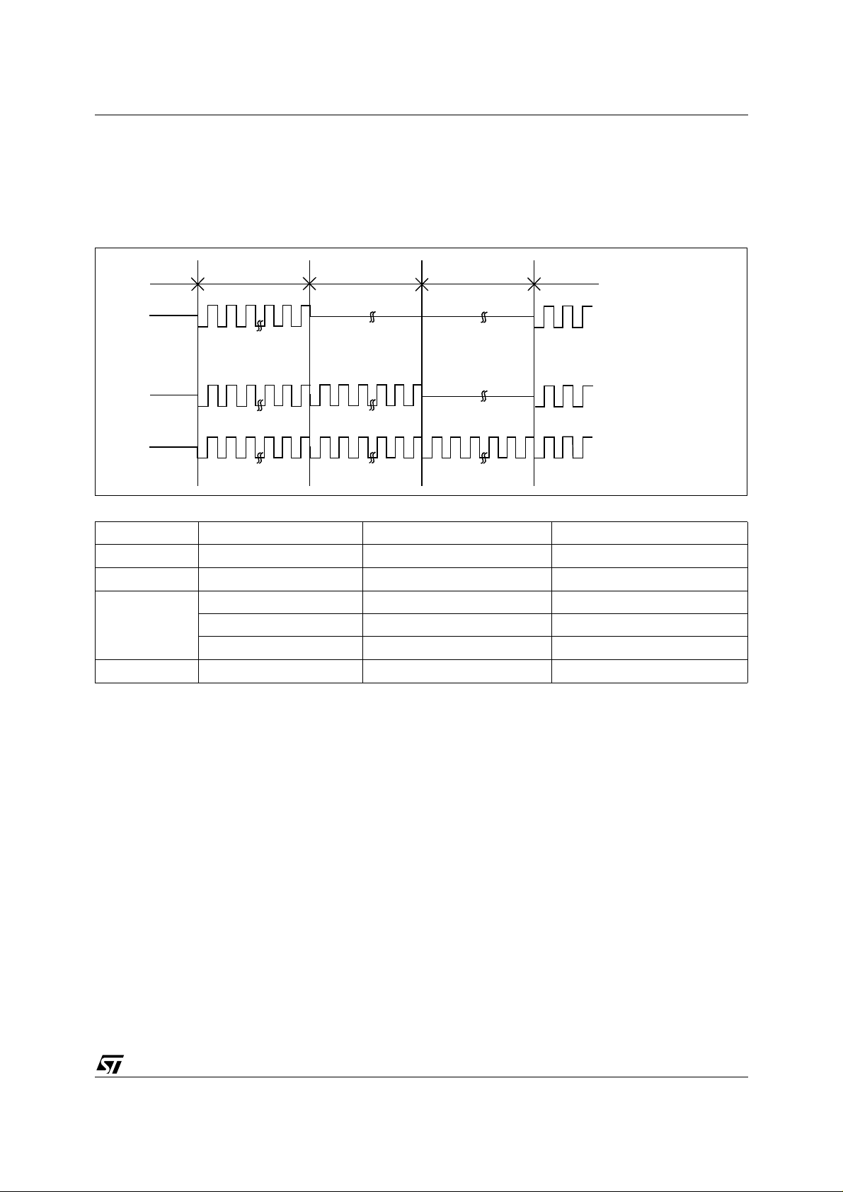
STV0299B
For t he “Unmodulated Tone Burst” Port C TRL 2 is
set to 0 and, only one byte, of value 00h is sent.
The parity bit is still 1, and as a r esult, the signal is
a continuous train of 12.5 ms. When the
alternatively to VDD and VSS levels. The DiSE qC
and Lock Control, DiSEqC FIFO and DiSEqC
Status Registers are in Addresses 08, 09 and
0Ah.
modulation is active, the DiSEqC output is driven
Figure 5:
Schematic showing Bit Transmiss ion
Idle 11 Periods 11 Periods 11 Periods Next bit
Transmission of 1’s
Transmission of 0’s:
a) PortCtrl2 = 1
b) PortCtrl2 = 0
Table 3:
PortCtrl (1:0) PortCtrl (2) FIFO Output
00 X empty 0
01 X empty 1
0 DATA = 00 Unmodulated tone burst
1 DATA = FFor00 Modulated tone burst
1 Note 1 DiSEqC signal
Note: 1
10
11 X XX Continuous tone
Byte to transfer in DiSEqC mode.
2
In mode PortCtrl (1:0)=10, the F22/DiSEqC pin returns to High -2 mode once the transmission is completed.
4.1.13 Standby Mode
A low power consumption mode (standby mode)
can be implemented (in this mode, f
standby mode, the I
2
C decoder still operates, but
with some restrictions (see Sections
4.1.5
).
Standby mode can be initiated or stopped by I
M_CLK
4.1.4
= 0). In
and
2
bus commands as described in MCR Register 02.
At power-on, the circuit starts to operate in
standby mode when the STDBY pin (pin 42) is
tied to V
. This guarantees low power
DD
consumption for the stand-alone modules
(PCMCIA size front-end modules) before any
command is initiated. After the power-on
C
sequence, the standby mode is entirely controlled
via MCR Register (02).
11/36
Page 12

STV0299B
4 FUNCTIONAL DESCRIPTION
(continued)
4.2 Signal Processing
4.2.1 I and Q Inputs
The ADC features differential inputs, but in most
applications I & Q signals are single-ended. In
such applications, I and Q signals from the tuner
are fed to the respectiv e IP and QP inputs through
a capacitor. The I
typically t o V
BOT
and QN pins are DC biased,
N
.The internal biasing of the ADC is
done on the circuit at the mid-voltage between
V
TOP
and V
BOT
.
The Input/Output Configuration Register is
described in Address 0Ch.
4.2.2 Main AGC (or AGC1)
The modulus of the I/Q input is compared to a
programmable threshold, m1, and the difference
is integrated. This signal is then converted into a
pulse density modulation signal to drive the AGC
output. It should be filtered by a simple analog
filter to control the gain command of any amplifier
before the A to D converter.
The output converter operates at f
M_CLK
/8 in order
to decrease the radiated noise and to simplify the
filter design. The output is a 5 V tolerant open
drain stage.
The reset value of the coefficient allows an initial
settling time of less than 100k master clock
periods.
The 8 integrator MSBs may be read or written at
any time by the microprocessor. When written, the
LSB’s are reset and the coefficient may be set to
zero by programming (in this case, the AGC is
reduced to a programmable 8-bit voltage
synthesizer).
The time constant of agc1 is estimated as
followed:
β
–
26
agc1
T
agc1
2
=
-----------------------
m1
×
T
M_CLK
with m1 = AGC1 reference level.
The AGC1 Control, AGC1 Reference and AGC1
Integrator Registers are in Addresses 0D and 0F.
4.2.3 Nyquist Root and Interpolation Filters
Two roll off values are available: 0.35 and 0.20.
Refer to the Input/Output Configuration Register
in Address 0C.
4.2.4 Offset Cancellation
This device suppresses the residual DC
component on I and Q. The compensation may be
frozen to its last value by resetting the DC offset
compensation bit in the AGC Control Register in
Address 0D.
4. 2.5 Signal AGC (o r AG C2)
The rms value of I and Q is me asured after the
Nyquist filter and compared to a programmable
value, m2, such as that of the main AGC.
The integrated error signal is applied to a
multiplier on each I and Q path.
The AGC2 Control Register is in Address 10.
Bits [7:5] give the AGC2 coefficient, which sets
beta_agc2, the gain of the integrator. Table 4
shows how beta_agc2 is programmed with AGC2
coefficient (which is related to the time constant of
the AGC).
Table 4:
AGC2 Coefficient beta_agc2
00
11
24
316
464
5 256
6N/A
7N/A
If AGC2 Coefficient = 0, the gain remains
unchanged from its last value.
The time constant is independent of the symbol
frequency, however it does depend on the
modulus, m1, of the input signal, programm ed in
AGC1, with the following approximate relation:
3
T
agc2
60 10
---------------------------------------------=
m1 beta_agc2
T
×
⋅
M_CLK
⋅
The AGC2 Integrator Registers (2 bytes - MSB
and LSB) are in Addresses 18 and 19. These
values may be read or written by the
microprocessor. When written, all the LSB’s
integrator bits are reset. This value is an image of
the signal power in the useful band. Compared
with the total power of the signal, the out-of-band
power may be computed (noise, or other channel).
12/36
Page 13

STV0299B
fn5.2 10
6
–
fSm2
β⋅⋅
=
β
2
beta_tmg
=
ξ
0.134 m2 2
alpha_tmg
⋅ ⋅
2
beta_tmg
--------------------------------------------------------------=
4 FUNCTIONAL DESCRIPTION
(continued)
4.3 Timing Recovery
4.3.1 Timing Control
The loop is parametrized by two coefficients:
alpha_tmg and beta_tmg. alpha_tmg can take
values from 0 to 4, and beta_tmg from 0 to 7
(Register 0E).
When the parameter is 0, the actual coefficient
value is zero. The 8 MSBs of the frequency
accumulator may be read or written at any time by
2
C bus—when written, all LSBs are reset.
the I
The Symbol Frequency Registers (MSB, Middle
Bits and LSB) are in Addresses 1F, 20 and 21.
These must be programmed with the expected
symbol frequency.
The units are:
f
M_CLK
----------------
20
2
Write mode is effective when writing the Middle Bit
Register. The MSB Register must be loaded
before the Middle Bit Register.
The value of the Timing Frequency Register , when
the system is locked, is an image of the frequency
offset. The unit is f
19
/2
(approx. 2 ppm). It should
S
be as close as possible to 0 (by adjusting symb ol
frequency register value) in order to have a
symmetrical capture range. R eading it allows for
optimal trimming of the timing range (Register
1A).
The actual symbol frequency is:
f
---------------------------------------------------------------------------------------=
S
act
where f
is the content of the symbol frequency
s_reg
register and T
f
⋅()
M_CLKfs_reg
the content of the timing
mg_reg
2f
⋅⋅()
+
sTmg_reg
20
2
frequency register.
4.3.2 Loo p Eq ua ti on
The timing loop may be considered as a second
order loop. The natural frequency and the
damping factor may be calculated using the
following formula:
where, f
is the symbol frequency, m2 is the AGC2
S
reference level and β is programmed by the timing
register:
The damping factor is:
where m2 is the reference level of the AGC2
register.
Table 5 shows the natural frequency in DVB, with
nominal reference level m2 = 20, for different
values of beta_tmg and alpha_tmg, without noise.
4.3.3 Timing Lock Indicator
The timing lock indicator reports a value
dependent upon the signal-to-noise ratio and on
the signal lock state.
With an AGC2 Reference level m2 = 20, if the
timing lock indicator is above 48, the timing is
locked; if it is above 42, this shows that a QPSK
signal is present, either locked with low C/N
(<3.6 dB) or unlocked with higher C/N; the
ambiguity may be solved by changing on purpose
the timing frequency of 1%; if it was locked before,
the indicator should be now under 42.
The indicator needs 30K symbols for stabilization
from unlock to lock after a frequency change.
The timing lock registers - the Timing Lock Setting
Register and the Timing Lock Indicator Regi ster are in Addresses 11 and 17.
Table 5:
beta_tmg
alpha_tmg 1234
Natural Frequency for
fS=20Mbaud
1 0.66 kHz 0.85 1.70 3.38 6.77
2 0.93 kHz 0.60 1.20 2.40 4.80
3 1.32 kHz 0.42 0.85 1.70 3.38
4 1.86 kHz 0.30 0.60 1.20 2.40
5 2.63 kHz 0.21 0.42 0.85 1.70
6 3.72 kHz 0.15 0.30 0.60 1.20
7 5.26 kHz 0.10 0.21 0.42 0.85
Damping Factor
13/36
Page 14

STV0299B
4 FUNCTIONAL DESCRIPTION
(continued)
4.4 Carrier Recovery and Derotator Loop
The tracking range of the derotator is ±f
(±f
/2). The initial frequency search may
sampling
M_CLK
/2
therefore be performed on several MHz ranges
without reprogramming the tuner.
Three phase detectors are selectable using
software:
• Phase detector algorithm 0: This algorithm
should only be used for BPSK reception.
• Phase detector algorithm 1: This algorithm is
used with QPSK reception, over a small range
of capture phases and with a channel noise
value over 4.5 dB.
• Phase detector algorithm 2: For QPSK
reception, it is used after locking, to minimize
the bit error rate in low channel noise
conditions. Algorithm 2 is recommended for
most applications.
The loop is controlled through α and
parameters.
The carrier loop control registers (the Alpha
Carrier Register, the Beta Carrier Register and the
Carrier Frequency Register) are in Addresses 13,
14, 22 and 23.
4.4.1 Loo p Para m et ers
Like the timing loop, the carrier loop is a
second-order system where two parameters,
and β, may be programmed with alpha_car and
beta_car respectively.
The natural frequency (f
fn7106–f
=
⋅⋅
n
M_CLK
) is:
m2
f
S
----------------
β⋅()
f
M_CLK
The damping factor is:
m2
-------- -
β
f
S
----------------
f
M_CLK
where
β
= ( 4+2c+d)
22 10
=
ξ
α
=(2+a)
⋅
2e, with e≥1. m2 is the reference
6–
⋅ ⋅
α
b
⋅
⋅
2
214, with b≥1, and
level in the AGC2 register.
4.4.2 Carrier Lock Detector
The carrier lock detector provides an indicator
with a high value when the carrier is locked,
dependent on the channel noise. When the carrier
is not locked, the indicator value is low.
The indicator value is compared to a
programmable 8-bit threshold (Register 15h). The
result of this comparison (1 if greater than the
threshold, else 0 if not) is written as the Carrier
Found flag (CF), and may be read in the status
register. The CF signal may be permanently
routed on the output LOCK (see Register 08h).
The Lock Detector Threshold Register and Lock
Detector Value Register are in Addresses 15 and
1C.
4.4.3 Derotator Frequency
The derotator frequency can be either measured
(read operation) or forced (write operation).
kHz
Derot_freq
=
------------------------------
2
16
f
()
⋅
M_CLK
freq
()
Derot_freq is a 16-bit signed value.
The Derot_freq Registers are Registers 22 and
23.
β
4.4.4 Carri er Frequency Off set Detecto r
The carrier recovery loop features a carrier
frequency offset detector and two phase
detectors. When the carrier frequency offset
detector is enabled, the central loop frequency is
modified proportionally to the carrier offset. The
gain and time constants of the dete ctor are set by
CFD[6:4] and CFD[3:2] respectively. When the
carrier loop is about to “phase lock” with the
α
carrier, the frequency detector stops automatically
and the phase lock is ensured by the selected
phase detector. This switchover point is
determined by the threshold CFD [1:0].
For stability reasons, the gain CFD [6:4] should
not exceed the coefficient e[3:0] of Register
BCLC.
The carrier frequency offset detector is in Address
12.
4.5 Noise Indicator
The noise indicator may be used to facilitate the
antenna pointing or to give an idea of the RF
signal quality and of the front-end installation
(dish, LNB, cable, tuner or ADC).
A simple C/N estimator can be easily
implemented by comparing the current indications
with a primarily-recorded look-up table.
The time constant ranges from 4 k to 256 k
symbols. The 16 MSB of the result may be read by
the microprocessor (Registers 24 and 25).
kHz
14/36
Page 15

STV0299B
4 FUNCTIONAL DESCRIPTION
4.6 Forward Error Correction
4.6.1 FEC Modes
Since the STV0299B is a multistandard decod er,
several combinations are possible, at different
levels:
• The demodulator may accept either QPSK or
BPSK signals - the only impact is on the carrier
algorithm choice (refer to Chapter 4.4).
The algorithm choice also affects the carrier
lock detector and the noise evaluation.
• There two primary options co ncerning t he FEC
operation - between DVB, DSS and Reser ved
Mode.
• There are two options concerning the FEC
feeding. The first is IQ flow, wh ich is the usual
case in QPSK modes DVB or DSS. The second
mode is I-only fl o w, used for BPSK.
The FEC Mode Register is in Address 28.
In Modes DVB and DSS, data is fe d to the Viterbi
decoder. Other parts of the decoding (such as the
Convo luti onal De interleaver) may be bypa s sed.
4.6.2 Viterbi Decoder and Synchronization
The convolutive codes are generated by the
polynomial G
modes DVB or DSS.
The Viterbi decoder computes for each symbol
the metrics of the four possible paths, proportional
to the square of the E uclidian distance between
the received I and Q and the theoretical symb ol
value.
The puncture rate and phase are estimated on the
error rate basis. Several rates are allowed and
may be enabled/disabled through register
programming:
• 1/2, 2/3, 3/4, 5/6, 7/8 in DVB.
• 1/2, 2/3, 3/4, 5/6 and 6/7 in DSS.
For each enabled rate, the current error rate is
compared to a programmable threshold. If it is
greater than this threshold, another phase (or
another rate) is tried until the right rate is obtained.
A programmable hysteresis is added to avoid
losing the phase during short term perturbation.
The rate may also be imposed by external
software, and the phase is incremented only upon
request by the microprocessor. The error rate may
be read at any t ime in order to use an algorithm
other than that implemented.
The Viterbi decoder produces an absolute
decoding. The decoder is controlled via several
Viterbi Threshold Registers (Registers 29, 2A, 2B,
= 171 octets and Gy = 133 octets in
x
(continued)
2C and 2D). For each Viterbi Threshold Register,
bits 6 to 0 represent an error rate threshold - the
average number of errors occurring during 256-bit
periods. The maximum programmable value is
127/256 (higher error rates are of no practical
use).
The Puncture Rate and Synchro Register
Address 31.
The automatic rate research is only done through
the enabled rates (see the corresponding bit set in
the Puncture and synchro register). In DSS, the
puncture rate 6/7 replaces the puncture rate 7/8.
In DSS, it is recommended that you disable
puncture rates 3/4 and 5/6 in order to save time in
the synchronization process.
The VSEARCH Register is in Address 32.
VSEARCH bit 7 (A/M) and bit 6 (F) programs the
automatic/manual (or computer aided) search
mode as f ollows:
• If A/M =0 and F=0, automatic mode is set.
Successive enabled punctured rates are tried
with all possible phases, until the system is
locked and the block synchro found. This is the
default (reset) mode.
• If A/M=0 and F=1, the current p uncture rate is
frozen. If no sync is found, the phase is
incremented, but not the rate number.
This mode allows shortening of the recovery
time in case of noisy condi tions. The puncture
rate is not supposed to change in a given
channel. In a typical computer-aided
implementation, the research begins in
automatic mode. The microprocessor reads the
error rate or the PRF flag in order to detect the
capture of a signal, then it switches F to 1, until
a new channel is requested by the remote
control.
• If AM=1 manual mode is set. In this cas e, only
one puncture rate should be validated the system is forced to this rate, on the current
phase, ignoring the time-out register and the
error rate. In this mode, each 0 to 1 transition of
the bit F leads to a phase incrementation,
allowing full control of the operation by an
external microprocessor by choosing the lowest
error rate.
The reset values are A/M=0, and F=0 (automatic
search mode).
The VERROR Register (a read only register) is in
Address 26. The last value of the error rate may
be read at any time in the register. Unlike the VTH,
the possible range is from 0 to 255/256.
The VSTATUS Register (a read only register)
Address 1B.
is in
is in
15/36
Page 16

STV0299B
x8x4x3x210
=++++
x15x141
++
4 FUNCTIONAL DESCRIPTION
(continued)
4.6.3 Synchronization
In DVB, the packet length after inner decoding is
204. The sync word is the first byte of each
packet. Its value is Hex 47, but this value is
complemented every 8 packets. In DSS, the
packet length is 147 and the sync word is Hex 1D .
An Up/Down Sync counter counts whenever a
sync word is recognized with the correct timing,
and counts down during each missing sync word.
This counter is bounded by a programmable
maximum - when this value is reached, the LK bit
(“locked”) is set in the VSTATUS register. When
the event counter counts down to until 0, this flag
is reset.
4.6.4 Error Moni toring
A 16-bit counter, ERRCNT, allows the counting of
errors at diff erent le ve ls . ERRCNT is f ed either by:
• the input QPSK bit errors (that are corrected by
the Viterbi decoder), or,
• the bit, or,
• the byte error (that are corrected by the
Reed-Solomon decoder), or,
• the packet error (not corrigible, leading to a
pulse at the ERROR output).
The content of ERRCNT may be transf e rred to the
read only registers ERRCNT_LOW (LSB) and
ERRCNT_HIGH (MSB).
Two functional modes are proposed, depending
on a control register bit:
1 Error Mode = 0. This is an error rate measure,
that tells the number of errors occurring within
a specified number of output bytes, NB. NB has
four possible values given in the Error Control
Register in Address 34. Every NB bytes, the
state of the error counter is transferred to a
16-bit register, then the error counter is reset.
The Error Count Registers in Addresses 1D
and 1E may be read by the microprocessor via
2
C bus. Two ways of reading may be used:
I
16-bit reading, starting with MSB, or 8-bit
reading (LSB only or MSB only).
2 Error Mode = 1. The error counter just counts
the error ; the I
2
C register permanently copies
the content of the error counter. When the MSB
byte is read, the error counter is reset. In both
modes, the 16-bit counter is saturated to its
maximum value.
4.6.5 Convolutional Deinterleaver
In DVB, the convolutional deinterleaver is 17 x 12.
The periodicity of 204 bytes per sync byte is
retained. In DSS, the convolutional deinterleaver
is 146 x 13, and there is also a periodicity of
147 bytes per sync byte. The deinterleaver may
be bypassed - for details, see Section 4.6.6
‘Reed-Solomon Decoder and Descrambler’
.
4.6.6 Ree d-S ol om on Decode r and
Descrambler
The input blocks are 204-byte long with 16 pari ty
bytes in DVB. The sy nc hro byte is t he fi rst byte of
the block. Up to 8 byte errors may be fixed.
The Code Generator polynomial is:
gx()x
=
()xω
0
ω
–
1
()……()xω
–
()
–
15
over the Galois Field generated by:
Energy dispersal descrambler and output energy
dispersal descrambler generator:
The polynomial is initialized every eight blocks
with the sequence 100101010000000.
The synchro words are unscrambled and the
scrambler i s re set every 8 p a ckets.
The output interface may be forced into high
impedance mode by setting bit 0 o f Address 28.
Doing this affects the D[7:0], CLK_OUT,
STR_OUT , D/P and ERROR pins. This also allo ws
for board testing, and “OR” wiring several link
circuits (for example, cable links). The output
stream is either parallel (byte stream) or serial (bit
stream) depending on bit 1 of Address 28.
The outputs are controlled by the RS Control
Register in Address 33.
4.6.7 Parallel Output Interface
A schematic diagram of the parallel output
interface is shown in Figure 7. The parallel output
format is compliant with the DVB common
interface protocol.
When the SYNC is not found (LK = 0 in the status
register), D/P (corresponding to the MiVAL signal
of the DVB common interface standard) remains
at a low level.
CLK_OUT has a duty cycle between 40 and 60%.
16/36
Page 17

STV0299B
C
4 FUNCTIONAL DESCRIPTION
(continued)
4.6.8 Serial Output Interface
The serial output interface is shown in Figure 6.
The serial bit stream is available on D7,
where MSB is first to reconstruct the original
order. If RS0 = 0, then the parity bits are output
(Register 33). If RS0 = 1, the data is null duri ng
the parity time slots.
STR_OUT is only high dur ing the first bit of each
packet, instead of during the first byte in parallel
mode.
ERROR has the same function as in parallel
mode.
CLK_OUT is the serial bit clock; it is derived from
either the master clock, M_CLK, (if SerClk = 0 in
Registers 02 and B3), or from the internal VCO
frequency divided by 6, (if SerClk = 1), by skipping
some pulses to accommodate the frequency
difference.
Figure 6:
Serial Output Interface
STR_OUT
CLK_OUT
D/P
D7
RS1 = 1
RS1 = 0
First bit of the packet
RS0 = 0
RS0 = 1
All of the outputs are synchronous of the same
master clock edge.
D0, STR_OUT, D/P and ERROR may be properly
sampled externally by the rising edge of
CLK_OUT, if RS1 = 0, or by the falling edge of
CLK_OUT if RS1 = 1. This clock runs
continuously, even during parity data, whatever
the value of RS0.
The first bit detected in a valid packet may be
decoded if it is found on the appropriate edge of
CLK_OUT, where STR_O UT = 1, ERROR = 0,
D/P = 1. The following bits only require the
assertion of D/P (while D/P = 1,...).
Outputs D0 to D6 remain at low level in serial
mode.
or 6/f
1/f
M-CLK
Data Parity
VCO
ParityUseful Data
ERROR
Figure 7:
D/P
STR_OUT
ERROR
Parallel Output Interface
RS1 = 0
LK_OUT
RS1 = 1
RS0 = 0
RS0 = 1
RS0 = 0
RS0 = 1
RS0 = 0
RS0 = 1
RS0 = 0
RS0 = 1
1 Packet
No Error Uncorrectib le Packet No Error
Data
Parity
17/36
Page 18

STV0299B
Table 6: Functi onal I2C Register Map
Name Address bit7 bit6 bit5 bit4 bit3 bit2 bit1 bit0
ID $00(r/w) Chip iden tif i cation numb er Release number
RCR * $01(w) K(1:0) dirclk M(4:0)
MCR * $02(w) stdby VCO off serclock P(2:0)
ACR * $03(w) prescaler divider
F22FR $04(w) frequency register f_reg(7 :0)
12CRPT $05(w) 12CT T- constan t T- co nstant SCLT value SDAT val ue
DACR1 $06(w) DAC mode DAC(11:8)
DACR2 $07(w) DAC(7:0)
DiSEqC $08(w ) LOCK output LOCK co nf DiSEqC DiSEqC mode
DiSEqC FIFO $09(w) DiSE1C FIFO1(7:0)
DiSEqC Status $0A(r) IP
IOCFG $0C(w)
AGC1C $0D(w) DCadj beta_agc1(2:0)
RTC $0E(w) alpha_tmg(2:0) beta_tmg(2:0)
AGC1R $0F(w) Iagc Reference Value
ACG2O $10(w) AGC2 coeff(2: 0) ACG2_Ref
TLSR $11(w) step_minus(3:0) step_plus(3:0)
CFD $12(w) FD on/off beta_fd FDTC LDL
ACLC $13(w) derot on/off noise_TC al pha_car
BCLC $14(w) Ph_detect_algo beta_car
CLDT $1 5(w) Lock detector threshold
AGC1I $16(r/w) AGC integrator value
TL1R $17(w) Timing lock indicator(7:0)
ACG2I1 $1 8(r/w) ACG2 integrator MSB
ACG2I2 $1 9(r/w) ACG2 integrat or LSB
RTF $1A(r/w) Timing loo p frequency (7:0)
VSTATUS $1B(r) CF PRF LK PR(2:0)
CLDI $1C(r) Lock detector integrator
ECNTH $1D(r) Error count MSBs
ECNTL $1E(r) Error count LSBs
SFRH $1F(w) Symb_freq(19:12)
SFRM $20(w) Symb_freq(11:4)
SFRL $21(w) Symb_freq(3:0)
CFRM $22(r/w) Carrier frequency register MSB
CFRL
NIRH
NIRL
VERROR
FECM
VTH0
VTH1
VTH2
VTH3 $2C(w) t3[6:0]
VTH4 $2D(w) t4[6:0]
PR $31(w) E4 E3 E2 E1 E0
V
SEARCH
RS $33(w) deint sync RS descram err bit MPEG clk pol clk cfg
ERRCNT $34(w) Errmode tsters Error source NoE
$23(r/w) Carrier frequen cy register LSB
$24(r) Noise indicator MSBs
$25(r) Noise indicator LS B s
$26(r) Error value
$28(w) FEC mode out type out imp
$29(w) t0[6:0]
$2A(w) t1[6:0]
$2B(w) t2[6:0]
$32(w) A/M F SN(1:0) TO(1:0) H(1:0)
OP1_
opdrain
SDAT input
status
OP1_1
OP0_
opdrain
FE FF
OP01 Nyquist filter I/Q conv
18/36
Page 19

5REGISTER LIST
Note:
All regist er addresses are hexadecim al val ues. Signed re gi sters are 2’s complement. All registers are read/write registers except
those specifically flagged as read-only (RO). All registers not listed in the below table, between 0 and 4E, should be programmed to
0.
STV0299B
Name
HEX
Address
IDENTIFICATION REGISTER (Read Only)
Reset
Value
Bit
Position
(refer to
Section 4.1.6
Signal Description
on page 8
)
ID 00 A1 [ 7:0] Gives the release number of the cir cuit in order to ensure software
compatibility.
REFERENCE CLOCK REGISTER
RCR 01 18 or 38 [7:6]
MASTER CLOCK REGISTER
(refer to
MCR 02 34 or B4 7
(refer to
[4:0]
Section 4.1.8
Section 4.1.8
K[1:0]
DIRCLK
5
M[4:0]
STDBY
VCO ON/OFF
6
on page 8
)
(Reset value depends on the polarity of DIRCLK-DIS pin).
on page 8
)
(Reset value depends on the polarity of STDBY pin).
0: ON
1: OFF
[5:4] These bits must be programmed to one.
SERCLK
3
0: Maximum instantaneous SERCL = Master Clock
F
VCO
-----------------
6
[2:0]
1: Maximum instantaneous SERCL =
P[2:0]
VC0 to M_CLK divider
19/36
Page 20

STV0299B
5REGISTER LIST
Name
AUXILIARY CLOCK REGISTER
ACR 03 2A [7:0]
(continued)
HEX
Address
Reset
Value
(refer to
Bit
Position
Section 4.1.8
on page 8
ACR Prescaler and Divider
This register is made up of the ACR [7:5] Prescaler field and the ACR
[4:0] Divider fie ld. The values in these fields c onfigure the auxiliary
clock function, the prescalar value, the clock signal frequency.
The frequency range is given for f
ACR [7:0] Function Prescaler Signal Frequency Range
000XXXX0
000XXXX1
001XXXXX
010XXXXX
011XXXXX
100XXXXX
101XXXXX
110XXXXX
111XXXXX
Output
Output
generator
generator
generator
generator
generator
generator
generator
In the LF generator, the programmable division factor is
32 + ACR[4:0]. In the HF generator, it is simply ACR[4:0]. This allows
the building of any frequency from 24 Hz to 1.1 kHz (within ±1.5%) in
the full operating range. The output signal is square in all cases.
When the auxiliary register is written, the prescaler and the programmable divider are reset.
F22 FREQUENCY REGISTER
(refer to
Section 4.1.8
on page 8
F22FR 04 8E [7:0] The actual frequency is f
accessed, the divider by 16 (also common to AUX_CLK) and the
divider by R[7:0] are initialized.
2
I
CRPT REGISTER
2
CRPT
I
(refer To
Section 4.1.10
05 0F 7
on page 10
2
I
CT
2
1: I
C repeater
)
0: Output port
[6] Must be programmed to zero.
[5:4] Repeater response time; value does not matter if the external time
constant
250ns.
≤
[3] Must be programmed to zero.
2
SCLT Port value
1 This bit must be programmed to zero.
0
SDAT Port value
Port
Port
HF
LF
LF
LF
LF
LF
LF
)
Signal Description
)
N/A output port = 0 N/A
N/A output port = 1 N/A
1
64
128
256
512
1024
2048
VCO
=400MHz.
VCO
/8/ACR[4:0]
f
VCO
/8192/(32+ACR[4:0])
f
VCO
f
/16384/(32+ACR[4:0])
VCO
/32768/(32+ACR[4:0])
f
VCO
/65536/(32+ACR[4:0])
f
VCO
/131072/(32+ACR[4:0])
f
VCO
f
/262144/(32+ACR[4:0])
VCO
1.6 to
50 MHz
775 to
1525 Hz
388 to
762 Hz
194 to
381 Hz
97 to
190 Hz
49 to
95 Hz
24 to
47 Hz
/(128 R[7:0]). When this register is
20/36
Page 21

STV0299B
5REGISTER LIST
Name
DAC REGISTERS
DACR1 (MSB) 06 A2 [7:5]
DACR2 (LSB) 07 00 [7:0]
DISEQC AND LOCK CONTROL REGISTER
DiSEqC 08 60 [7:6]
DISEQC FIFO
DiSEqC FIFO 09 00 [7:0]
DISEQC STATUS
DiSEqC
Status
RESERVED
(refer to
(continued)
HEX
Address
(refer to
(refer to
0A R0 7
0B
Reset
Value
Section 4.1.11
Section 4.1.12
Section 4.1.12
Bit
Position
[3:0]
[4:3] These bits must be programmed to zero.
[1:0]
on page 10
on page 10
[5:2] Not relevant.
Signal Description
on page 10
4 This bit must be programmed to zero.
(refer to
5
2
6
1
0
)
DAC Mode
This field controls the DAC:
: Functions as output port. The DAC output permanently 0.
000
: Functions as output port. DAC output permanently 1.
001
: High impedance mode.
010
: Functions as DAC. Duty cycle modulated at f
100
: Functions as DAC. Duty cycle modulated at f
101
: Functions as DAC. Duty cycle modulated at f
110
: Reserved functions.
Other
DAC: 4 MSB
DAC: 8 LSB
Section 4.1.12
Lock Output
00: 0
01: 1
10: CF
11: LK
Lock Configuration
1: Open drain
0: Push-pull
DiSEqC/Unmodulated Burst
DiSEqC Mode
)
FIFO byte
)
Input Port
port for general use purposes.
SDAT Input State
FIFO empty
FIFO full
Reserved
: This bit gives the i nput level on the pin I P0. It is an input
on page 10
)
CLK
CLK
CLK.
/16.
/4.
21/36
Page 22

STV0299B
5REGISTER LIST
Name
INPUT/OUTPUT CONFIGURATION REGISTER
IOCFG 0C F0 7
AGC1 CONTROL REGISTER
AGC1C 0D 81 7
TIMING LOOP REGISTE R
RTC 0E 23 7 This bit must be programmed to zero.
AGC1 REFERENCE REGISTER
AGC1R 0F 54 7
AGC2 AND OFFSET CONTROL REGISTER
AGC2O 10 74 [7:5]
(continued)
HEX
Address
Reset
Value
(refer to
(refer to
(refer to
Bit
Position
(refer to
OP1 control
1: Open drain
0: Normal
6
OP1 value
5
OP0 control
1: Open drain
0: Normal
4
OP0 value
3 This bit must be programmed to zero.
[2:1]
Nyquist Filter
These bits determine Nyquist filter settings:
00 = raised cosine at 35%
01 = raised cosine at 20%
10 = reserved
11 = reserved
0 Bit 0 when se t, multiplies the data on th e Q input by -1 in order to
accommodate QPSK modu lation with a nother convention o f rotation
sense. This is equivalent to a permutation of I and Q inputs, or a spectral symmetry. This permutation is performed after derotation.
Section 4.2.2
DC offset compensation:
1: On
0: Off
[6:3] These bits must be programmed to zero.
[2:0]
Section 4.3.1
[6:4]
[2:0]
beta_agc1
on page 13
alpha_tmg
3 This bit must be programmed to zero.
beta_tmg
Section 4.2.2
Iagc
1: Invert
0: Normal
If Iagc is set, the outp ut signal is com plemented (i.e. a high value for
the AGC voltage will cause a high gain in the tuner).
6 This bit must be programmed to zero.
[5:0]
[4:0]
AGC1 Reference Value (m1).
(refer to
AGC2 Coefficient
AGC2_Ref (m2)
Section 4.2.1
on page 12
)
on page 12
Section 4.2.5
)
)
on page 12
Signal Description
on page 12
)
Refer to page 12.
)
22/36
Page 23

STV0299B
5REGISTER LIST
Name
TIMING LOCK SETTING REGISTER
TLSR 11 88 [7:4] Must be programmed to 8 (to be confirmed)
CARRIER FREQUENCY DETECTOR REGISTER
CFD 12 F7 7 1: Carrier Frequency Offset Detector coupled to Carrier recover loop
ALPHA CARRIER AND NOISE ESTIMATOR REGISTER
ACLC 13 88 7
BETA CARRIER REGISTER
BCLC 14 5C [7:6]
CARRIER LOCK DETECTOR THRESHOLD REGISTER
CLDT 15 14 [7:0] Signed Number
AGC1 INTEGRATOR REGISTER
AGC1I 16 [7:0]
TIMING LOCK INDICATOR REGISTER
TLIR 17 R0 [ 7:0] (Not Signed)
(continued)
HEX
Address
Reset
Value
(refer to
(refer to
Bit
Position
(refer to )
[3:0] Must be programmed to 4 (to be confirmed)
(refer to
0: Carrier Frequency Offset Detector disabled
[6:4] Gain for Carrier Frequency Offset Detector
[3:2] Time constant for Carrier Frequency Offset Detector
[1:0]
[5:4]
[3:0]
Chapter 4.4
[5:0]
Lock Detector thre shold to d isable the Ca rrier Freq uency Offse t
Detector:
00: -16
01: -32
10: -48
11: -64
Derotator On/Off
1: On
0: Off
6 This bit must be programmed to zero.
Noise Estimator Time Constant
00: 4 k symbols
01: 16 k symbols
10: 64 k symbols
11: 256 k symbols
alpha_car
Bits 3, 2 and 1: b[2:0]
Bit 0: a
on page 14
phase_detector_algo
Phase detector algorithm:
00: Algorithm 0 (BPSK application)
01: Algorithm 1 (QPSK application)
10: Algorithm 2 (QPSK application)
11: Reserved
beta_car
Bits 5 to 2: e[3:0]
Bit 1: c
Bit 0: d
Section 4.2.2
AGC Integrator Value
(refer to
Section 4.3.3
Chapter 4.4
(refer to
)
(refer to
on page 12)
on page 13
Signal Description
on page 14
Chapter 4.5
Section 4.4.2
(Signed Number)
)
)
on page 14
on page 14
)
)
23/36
Page 24

STV0299B
5REGISTER LIST
Name
AGC2 INTEGRATOR REGISTERS
AGC2I1 (MSB) 18 [7:0]
AGC2I2 (LSB) 19 [7:0]
TIMING FREQUENCY REGISTE R
RTF 1A [7:0] Signed Number
VSTATUS REGISTER (Read Only)
VSTATUS 1B RO 7
CARRIER LOCK DETECTOR VALUE REGISTER
CLDI 1C [7:0] Signed Number
ERROR COUNT REGISTERS
ERRCNT_HIGH 1D [7:0] MSB byte (Not Signed)
ERRCNT_LOW 1E [7:0] LSB byte (Not Signed)
SYMBOL FREQUENCY REGISTERS
SFRH 1F 80 [7:0]
SFRM 20 00 [7:0]
SFRL 21 00 [7:4]
CARRIER FREQUENCY REGISTER
CFRM 22 [7:0]
CFRL 23 [7:0]
NOISE INDICATOR REGISTERS (Read Only)
NIRH 24 RO [7:0]
NIRL 25 RO [7:0]
(continued)
HEX
Address
Reset
Value
(refer to
(refer to
(refer to
(refer to
Bit
Position
Section 4.2.5
AGC2 Integrator MSB Bits
AGC2 Integrator LSB Bits
Section 4.3.1
Section 4.6.3
Carrier Found Flag
When the Carrier Found (CF) flag (se e
set, it indicates that a QPSK signal is present at the input of the Viterbi
decoder.
[6:5] Not relevant.
4
Puncture Rate Found
The Puncture Rate Found (PRF) bit indic ates the state of the punc-
ture rate research: 0 for searching and 1 when found. This bit is irrele-
vant in manual mode.
3
Locked/Searching Sync Word
The LK bit indicates the state of the sync word search: 0 for searching
and 1 when found.
[2:0]
Current Puncture Rate, PR[2:0]
The Current Puncture Rate (CPR) bits hold the current puncture rate
indices, as follows:
100: Basic 1/2 (modes DVB and DSS) or Punctured 1/2 (reserved
000: Punctured 2/3
001: Punctured 3/4
010: Punctured 5/6
011: Punctured 7/8 (modes DVB and DSS) or 6/7 (reserved mode)
Section 4.6.4
(refer to
(refer to
Section 4.3.1
Symb_freq
The reset value of Hex 800000 corresponds to f
Symb_freq
Symb_freq
[3:0] These bits must be programmed to zero.
Chapter 4.4
Derotator Frequency (MSB) (signed value)
Derotator Frequency (LSB) (signed value)
(refer to
Noise Indicator (MSB)
Noise Indicator (LSB)
on page 12
on page 13
on page 16
mode)
(refer to
on page 16
Chapter 4.5
Section 4.4.2
)
on page 13
(MSBs)
(Middle SB
)
(LSB
S
on page 14
Signal Description
)
(Not Signed)
(Not Signed)
)
)
on page 14
)
)
S
)
on page 14
(Not Signed)
(Not Signed)
)
Chapter 4.4
)
on page 14 ) is
/2.
M_CLK
24/36
Page 25

STV0299B
5REGISTER LIST
Name
VERROR REGISTER (Read Only)
VERROR 26 RO [7:0]
FEC MODE REGISTER
FECM 28 01 [7:4]
VITERBI THRESHOLD REGISTERS
VTH0 29 1E [7:0]
VTH1 2A 14 [7:0]
VTH2 2B 0F [7:0]
VTH3 2C 09 [7:0]
VTH4 2D 05 [7:0]
PUNCTURE RATE AND SYNCHRO REGISTER
PR 31 1F [7:6:5] These bits must be programmed to zero.
(continued)
HEX
Address
(refer to
Reset
Value
(refer to
Section 4.6.1
Bit
Position
Section 4.6.2
Error Rate
on page 15
FEC Mode
This field indicates the FEC Operation mode and the FEC feeding.
0000: DVB (QPSK), FEC feeding IQ/IQ/IQ/IQ
0001: DVB (BPSK extension), FEC feeding IX/IX/IX/IX
001X: Reserved
0100: DSS, FEC feeding IQ/IQ/IQ/IQ
1XXX: Reserved
[3:2] These bits must be programmed to zero.
1
Output Type
1: Serial
0: Parallel
0
Output Impedance
1: High Impedance
0: Normal Impedance
(refer to
Section 4.6.2
Rate = 1/2 Threshold.
Rate = 2/3 Threshold.
Rate = 3/4 Threshold.
Rate = 5/6 Threshold.
Rate = 7/8 or 6/7 Threshold.
(refer to
4 Enable punctured rates 7/8 (in DVB) or 6/7 (in DSS).
3 Enable punctured rate 5/6.
2 Enable punctured rate 3/4.
1 Enable punctured rate 2/3.
0 Enable basic or punctured rate 1/2.
on page 15
(Not Signed)
)
on page 15
Section 4.6.2
)
)
on page 15
Signal Description
)
25/36
Page 26

STV0299B
5REGISTER LIST
Name
VITERBI AND SYNCHRO SEARCH REGISTER
VSEARCH 32 19 7
(continued)
HEX
Address
Reset
Value
Bit
Position
6Freeze
[5:4]
[3:2]
[1:0]
Signal Description
(refer to
0: Automatic search mode
1: Manual search mode
SN[1:0]
This is the averaging period. The field gives the number of bits
required to calculate the rate error.
00 = 1024
01 = 4096
10 = 16384
11 = 65536
Reset Value: SN = 01 (4096 bits)
TO[1:0]
This is the time out value (given in 1024-bit periods). This field is used
to program the maximum duration of the synchro word research in
automatic mode. If no sync is found within this duration, and if bit RS6
(Sync Enable) is set in the Re ed-Solomo n register, another phase o r
puncture rate is tried. If RS6 = 0, the time-out has no effect.
00 = 16
01 = 32
10 = 64
11 = 128
Reset Value: TO = 10 (64k bit periods)
H[1:0]
This is the hysteresis value. This fie ld is used to program the maxi -
mum value of the Sync counter. The unit is the block duration
(204 bytes in DVB, 147 in DSS).
00: 16
01: 32
10: 64
11: 128
Reset Value: H = 01 (32 blocks)
Section 4.6.2
on page 15
)
26/36
Page 27

STV0299B
5REGISTER LIST
Name
RS CONTROL REGISTER
RS 33 F8 7
(continued)
HEX
Address
Reset
Value
(refer to
Bit
Position
Section 4.6.6
6
5
4
3
2
1
0
Signal Description
on page 16
- Deinterleaver Enable
RS7
1: The input flow is deinterleaved.
0: The input flow is not affected.
- Synchro Enable
RS6
1: The synchro is processed.
0: The synchro word search is disabled. The bit-to-byte conversion
remains in its current phase regardless of whether the synchro
word is recognized o r not. This allows the use of the S TV0299BB
with inner convolutional coding only.
- Reed-Solomon Enable
RS5
1: The input code is corrected.
0: No correction happens, all the data is fed to the descrambler.
The error signal remains inactive.
- Descrambler Enable
RS4
1: The output flow from Reed-Solomon decoder is descrambled.
0: The descrambler is disactivated.
- Write Error Bit
RS3
1: If an uncorrectible erro r happens in DVB, the MSB of the first byte
following the sync byte is forced to 1 after descrambling.
0: The output flow is unchanged.
- Block Synchro
RS2
1: The first byte of each packet is forced to Hex 47 in mode A.
0: The first byte is the one that is r eceived. In DVB, it should be the
synchro byte, complemented every 8th packet.
- Output Clock Polarity
RS1
1: The data and control signals are clocked during the high-to-low
transition of CLK_OUT.
0: The data and control signals are clocked during the low-to-high
transition of CLK_OUT.
- Output Clock Signal Configuration during Parity Bytes
RS0
1: D[7:0] and ERROR are null during the parity bytes. If the packet
contains more than 8 errors, ERROR only rem ains high during the
data tran smiss ion. In pa rallel m ode, CL K_OU T rem ains low dur ing
the parity bytes. In serial mode, the output bit clock is always
running.
0: CLK_OUT is continuous and the par ity bytes are transm itted . If the
packet contains more t han 8 errors, ERROR remains hig h during
the entire packet.
)
27/36
Page 28

STV0299B
5REGISTER LIST
Name
ERROR CONTROL REGISTER
(continued)
HEX
Address
Reset
Value
(refer to
ERRCNT 34 01 7
Bit
Position
Section 4.6.4
on page 16
Signal Description
)
Error Mode
1: Error count
0: Error rate
6 This bit must be programmed to zero.
[5:4]
Error Source
The error sources are as follows:
00: QPSK bit errors
01: Viterbi bit errors
10: Viterbi byte errors
11: Packet errors.
[3:2] These bits must be programmed to zero.
[1:0]
NOE
The NOE bits represent the Count Period in bytes (NB):
12
bytes
00: 2
14
bytes
01: 2
16
bytes
10: 2
18
bytes
11: 2
28/36
Page 29

6 ELECTRICAL CHARACTERISTICS
STV0299B
6.1 Absolute Maximum Ratings
Maximum limits indicate where perm anent device
damages occur. Continuous operation at these
limits is not intended, and should be limited to
those conditions specified in Section 6.3
Electrical Characteristics’
.
Symbol Parameter Value Unit
V
DD_3.3 V
V
DD
V
I
V
O
T
stg
T
oper
T
Note: 1
(1)
(1)
j
Pad Power Supply Voltage 4.0 V
Core Level Power Supply Voltage 3.0 V
Voltage on Input Pins
Voltage on Output Pins
-0.5, V
-0.5, V
DD_3.3 V
DD_3.3 V
+0.5
+0.5
Storage Temperature -40, +150 °C
Operating Ambient Temperature -10, +70 °C
Junction Temperature +125 °C
Except for AGC, SDA, SCL, S DAT, SCLT pin, which can be connec ted to 5 V +10% via a resistor.
6.2 Thermal Data
Symbol Parameter Max. Value Unit
(4)
R
th(j-a)
R
th(j-c)
Note: 2
Note: 3
Junction-ambient Thermal Resistance
Junction-case Thermal Resistance 11 °C/W
Single-layer PCB.
Multi-layer PCB.
70
45
(5)
6.3 DC Electrical Characteristics
VDD = 2.5 V
Symbol Parameter Test Conditions Min. Typ. Max. Unit
V
DD_3.3 V
V
DD_core
V
DD_STDBY
I
DD
I
DDA
I
DD
I
DDA
, V
DD_3.3 V
= 3.3 V and T
Operating Voltage 3.0 3.3 3.6 V
Operating Voltage 2.3 2.5 2.7 V
V
DDA
Operating Voltage Circuit in stand-by 2.2 2.5 2.6 V
Operating Voltage Circuit in stand-by 2.3 2.5 2.7 V
30M
Average
30M Average V
45M
Average
45M Average V
I
DDsb
V
V
I
LK
V
OL
V
OH
IL
IH
Average Current in Standby Mode VCO stopped 0.5 4 mA
Low Level Input Voltage
High Level Input Voltage 2.0
Input Leakage Current 3.6 V 1
High Level Output Voltage
Low Level Output Voltage
amb
V
V
Current
DD_2.5V
Current V
DDA
Current
DD_2.5V
Current V
DDA
=25°C unless otherwise specified.
V
V
V
DD_3.3 V
I
SOURCE
DD=2.7V
DD=2.6V
DD=2.7V
DD=2.6V
= 76MHz
= 76MHz
= 88MHz
= 88MHz
= 3.3 V - 10%
=1.6mA
200 mA
50 mA
240 mA
50 mA
0.8 V
2.4
0.4
‘DC
V
V
°C/W
V
A
µ
V
V
29/36
Page 30

STV0299B
6 ELECTRICAL CHARACTERISTICS
6.3 DC Electrical Characteristics
VDD = 2.5 V
, V
DD_3.3 V
= 3.3 V and T
(continued)
(continued)
=25°C unless otherwise specified.
amb
Symbol Parameter Test Conditions Min. Typ. Max. Unit
RESET
V
ILT
V
IHT
Low Level Threshold Falling Input
High Level Threshold Falling Input
0.8
2.0
CLK_IN
V
IL
V
IH
C
IN
Low Level Input Voltage
High Level Input Voltage
0.8
2.0
Input Capacitance 3 pF
AGC/SDA/SCL/SDAT/SCLT
V
OIL
I
LK
Low Level Output Voltage
Input Leakage Current V
I
SINK
AGC
=2mA
=5.5V
0.4 V
4.0
A/D CONVERTER
V
V
V
TOP
BOT
R
C
in
in
in
Differential Input Voltage 0.4 0.5 0.8
High Voltage Reference 1.5 V
Low Voltage Reference 1 V
DC Input Resistance I/Q Inputs
10
6
∞Ω
Input Capacitance I/Q Inputs 5 pF
INL Integral Non-Linearity -1.5 +1.5 LSB
DNL Differential Non-Linearity -0.8 +0.8 LSB
SNR Signal to Noise Ratio 30 33 36 dB
N
eff
Effective Number of bits
(1)
5.0 5.5 6.0 bits
V
V
V
V
A
µ
V
pp
Note: 1
30/36
Test conditions: F
= 52MHz, FIN = 8MHz, VIN = 0.5 Vpp
clock
Page 31

STV0299B
CLK_OUT
D7, D/P.
STR_OUT,
ERROR
t
CKH
t
CKSU
CLK_OUT
D7, D/P.
STR_OUT,
ERROR
t
CKH
t
CKSU
6 ELECTRICAL CHARACTERISTICS
(continued)
6.4 Timing Characteristics
Symbol Parameter Min. Typ. Max. Unit
f
VCO
f
CLK_IN
PARALLEL OUTPUT D[7:0], D/P, CLK_OUT, STR_OUT, ERROR OUTPUT CHARACTERISTICS
Bit RS1 = 1 in RS CONTROL REGISTER (Address 33). Refer to Figure 8
t
CLK_duty
t
CKSU
t
CKH
D[7:0], D/P, STR_OUT, ERROR stable before CLK_OUT
D[7:0], D/P, STR_OUT, ERROR stable after CLK_OUT
Bit RS1 = 0 in RS CONTROL REGISTER (Address 33). Refer to Figure 9
t
CKSU
t
CKH
D[7:0], D/P, STR_OUT, ERROR stable before CLK_OUT
D[7:0], D/P, STR_OUT, ERROR stable after CLK_OUT
SERIAL OUTPUT D7, D/P, CLK_OUT, STR_OUT, ERROR OUTPUT CHARACTERISTICS
Bit RS1 = 1 in RS CONTROL REGISTER (Address 33). fM.CLK = 90MHz. Refer to Figure 10
t
CKSU
t
CKH
D7, D/P, STR_OUT, ERROR stable before CLK_OUT
D7, D/P, STR_OUT, ERROR stable after CLK_OUT
Internal VCO frequency 300 400 MHz
CLK_IN or XTAL frequency 4 30 MHz
CLK_OUT duty cycle 40 50 60 %
(1)
Falling Edge
Falling Edge
Falling Edge
Falling Edge
Falling Edge
Falling Edge
2*Tm
(1)
2*Tm
(1)
2*Tm
(1)
2*Tm
3.5 ns
3ns
ns
ns
ns
ns
t
CKSU
t
CKH
Note: 1
Tm = Master clock period in ns
Figure 8:
CLK_OUT
D[7:0], D/P.
STR_OUT,
ERROR
Figure 9:
CLK_OUT
D[7:0], D/P.
STR_OUT,
ERROR
Bit RS1 = 0 in RS CONTROL REGISTER (Address 33). fM.CLK = 90MHz. Refer to Figure 11
D7, D/P, STR_OUT, ERROR stable before CLK_OUT
Falling Edge
D7, D/P, STR_OUT, ERROR stable after CLK_OUT
Falling Edge
3.5 ns
2ns
Figure 10:
t
CKSU
t
CKH
Figure 11:
t
CKSU
t
CKH
31/36
Page 32

STV0299B
6 ELECTRICAL CHARACTERISTICS
2
C Bus Characteristics
6.5 I
(continued)
Symbol Parameter Test Conditions Min. Typ. Max. Unit
V
IL
V
IH
V
OH
V
OL
I
LK
C
IN
I
OL
f
SCLN
f
SCLS
t
BUF
t
HD, STA
t
LOW
t
HIGH
t
SU, STA
t
SU, STO
t
SU, DAT
t
, t
R
C
B
Bus Free Time between a STOP and START
Hold Time (repeated) ST ART Condition. After
this period, the first clock pulse is generated.
Setup Time for a repeated START Condition 0.6
Rise and Fall Time of both SDA and SCL sig-
F
Low Level Input Voltage
High Level Input Voltage
High Level Output Voltage
Low Level Output Voltage
Input Leakage Current
Pull up to 5 V ±10%
Pull up to 5 V ±10%
= 0 V to 5 V
V
IN
-0.5
2.0
-10 10
0.8
5.5
5.5
0.4
Input Capacitance 0 3.5 pF
Output Sink Current
SCL Clock Frequency
V
OL
Normal Mode
Standby Mode
0
0
10 mA
/40
f
M_CLK
/10
f
CLK_IN
=0.5V
1.3
Condition
0.6
Low Period of the SCL Clock
High Period of the SCL Clock
1.3
0.6
Setup Time for STOP Condition 0.6
Data Setup Time 100 ns
300 ns
nals
Capacitive Load for each Bus Line 400 pF
V
V
V
V
A
µ
-
s
µ
s
µ
s
µ
s
µ
s
µ
s
µ
Figure 12:
SDA
SCL
2
C bus timing diagram
I
t
BUF
t
HD,STA
t
LOW
t
SP
t
SU,STO
t
HIGH
t
F
t
SU,DAT
t
SU,STA
t
HD,STA
t
R
32/36
Page 33

7 APPLICATION BLOCK DIAGRAMS
STV0299B
Figure 13:
Application Block Diagram
ZIF or
Double Conversion
to PLL Synthesizer
LNB Supply
AGC Control
4 MHz
I
Dual
Q
2
ADC
2
C Repeater
I
DiSEqC
I/O +
AGC1
2
I
C
QPSK
FEC
Serial or
Parallel
4 serial or 12 parallel
To Transport IC
33/36
Page 34

STV0299B
7 APPLICATION BLOCK DIAGRAMS
Typical Application Diagram
ZIF tuner or convential tuner
5V 5V 5V 30V
5V
22k
Ω
10k
Ω
10nF
4MHz
22 pF 22 pF
Ω
OLF
2V5A
2V5D
2V5D
3V3
LNBP 15SP
2x
2.2µF
10nF
22V
10k
12
3W
Ω
Ω
2V5D
10k
100 nF
10k
Ω
(continued)
5V
R≤10K
R
100 nF
100 nF
(option)
4MHz
Clock
2V5D 2V5D
64 63 62 61 60 59 58 57 56 55 5054 53 52 51 49
1
2
3
4
5
6
7
8
9
10
11
12
13
14
15
16
17 18 19 20 21 22 23 24 25 26 3127 28 29 30 32
R
2V5A
STV0299
B
3V3 2V5D
2x
47 pF
2x
470
2V5A
120
Ω
5%
Ω
120
Ω
2 x
100 nF
5%
120
Ω
5%
48
2V5A
47
46
45
44
43
42
41
2V5D
40
39
OLF
38
37
36
35
34
33
RESET
Requirements
the analog ground must be connected
by only one track.
: The digital ground and
34/36
SDA
SCL
Error
D/P
STR_OUT
CLK_OUT
Serial Clock
CONTROL Serial
DATA O/P
12x47
Ω
D7 D0
ParallelD A TA O/P
Symbols:
Serial Data
this symb o l represents a
Digital ground
this symb o l represents an
Analog ground
Page 35

8 PACKAGE MECHANICAL DATA
STV0299B
64 Pins Thin Plastic Quad Flat Pack (TQFP No Slug)
64 49
1
16
17 32
e
D3
D1
D
A
A2
A1
0,10 mm
.004 inch
E
E1
L1
L
K
SEATING PLANE
0,25 mm
.010 inch
GAGE PLANE
B
c
48
E3
33
Millimeters Inches
Dimensions
Min. Typ. Max. Min. Typ. Max.
A 1.60 0.063
A1 0.05 0.15 0.002 0.006
A2 1.35 1.40 1.45 0.053 0.055 0.057
B 0.17 0.22 0.27 0.007 0.009 0.011
C 0.09 0.20 0.004 0.008
D 12.00 0.472
D1 10.00 0.394
D3 7.50 0.295
e 0.50 0.0197
E 12.00 0.472
E1 10.00 0.394
E3 7.50 0.295 -
L 0.45 0.60 0.75 0.018 0.024 0.030
L1 1.00 0.039
K0° (Min.), 7° (Max.)
35/36
Page 36

STV0299B
Information furnished is believ ed to be accurate and reliable. H owever, STMicroelectronics a ssumes no responsibility f or the
consequences of use of such informat ion nor for a ny infrin gement of pat ents or other rights of third parties which m ay result
from its use. No license is granted by implication or otherwise under any patent or patent rights of STMicroelectronics.
Specifications mentioned in this publication are subject to change without notice. This publica tion supe rsed es an d replaces all
information previously suppl ied. STMi croelectronics products are not authorized f or use as critical components in life s upport
devices or systems without express written approval of STMicroelectronics.
The ST logo is a trademark of STMicroelectronics.
DSS
© 2000 STM ic r o el e ctronics - All Rights R eserved
STMicroelectronics GROUP OF COMPANIES
Australia - Brazil - China - Finlan d - F rance - Germany - Hong Ko ng - India - Italy - Japan - Mal aysia - Malta - M orocco
Singap ore - Spain - Sweden - Switzerland - United Ki ngdom - U.S. A.
TM
DiSEqC
is a tradem ar k of EUTELSAT.
TM
is a trademark of Hughes Inc. (USA).
http://www.st.com
36/36
 Loading...