

Page 1
DUAL40 MSPS 6-BIT ANALOG TO DIGITALCONVERTER
.
RESOLUTION6-BIT
.
MAX. SAMPLINGFREQUENCY: 40 MSPS
.
TTLDATAOUTPUTS
.
BUILT-INSAMPLINGANDHOLD CIRCUIT
.
DUAL ADC ON CHIP TO IMPROVE CHANNELMATCHING
APPLICATIONS
.
QPSK DEMODULATION IN A SATELLITE
DECODER
DESCRIPTION
The STV0190 is a dual 40 MSPS 6-bit Analog to
Digital converter.
It is dedicated to QPSK demodulation in Satellite
receiver.
The Flasharchitecturecombined with interpolation
technic gives the best trade off between power
consumption and maximum conversionspeed.
STV0190
ADVANCE DATA
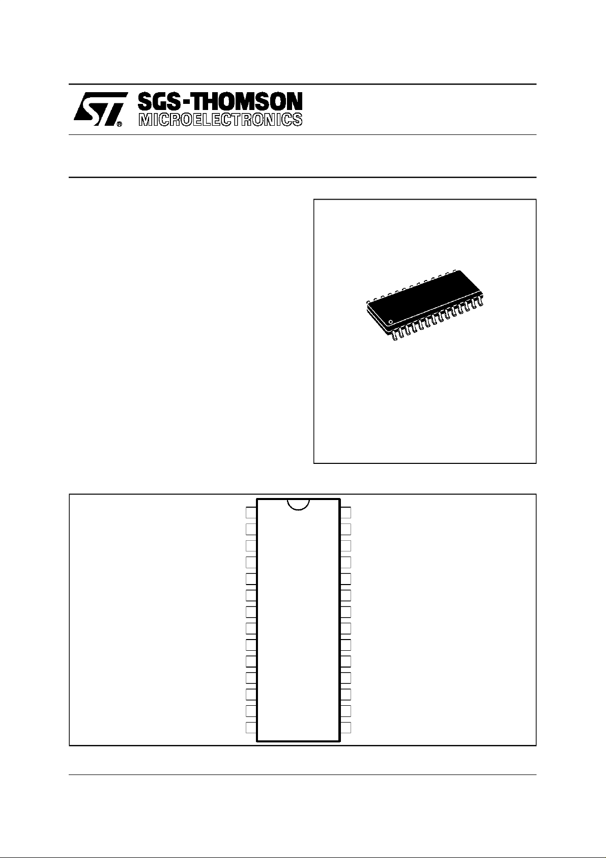
SO28
(Plastic Micropackage)
ORDER CODE : STV0190
PINCONNECTIONS
V
CCO
OGND
AGND
V
TOP
V
V
MIDA
V
MIDB
V
V
BOT
V
CCA
DGND
V
CCD
CLKIN
OGND
May 1996
Thisis advance information ona newproduct nowin developmentor undergoing evaluation.Details are subject to changewithout notice.
1
2
3
4
5
INA
6
7
8
INB
9
10
11
12
13
14
28
27
26
25
24
23
22
21
20
19
18
17
16
15
D5B
D4B
D3B
D2B
D1B
D0B
D5A
D4A
D3A
D2A
D1A
D0A
CLKOUT
V
CCO
0190-01.EPS
1/7
Page 2
STV0190
PIN CONFIGURATION
Pin N° Symbol Function
1V
CCO
2 OGND Output Buffer Ground Channel A + B
3 AGND Analog Ground
4V
5V
6V
7V
8V
9V
10 V
TOP
INA
MIDA
MIDB
INB
BOT
CCA
11 DGND Digital Ground
12 V
CCD
13 CLKIN Clock Input
14 OGND Output Buffer Ground Channel A + B
15 V
CCO
16 CLKOUT Clock Output
17 to 22 D0A to D5A D0 (LSB) to D5 (MSB) Outputs Channel A
23 to 28 D0B to D5B D0 (LSB) to D5 (MSB) Outputs Channel B
Output Buffer Supply Voltage Channel A + B
Top Reference Voltage
Analog Input Channel A
Reference Voltage DC CouplingChannel A
Reference Voltage DC CouplingChannel B
Analog Input Channel B
Bottom Reference Voltage
Analog Supply Voltage
Digital Supply Voltage
Output Buffer Supply Voltage Channel A + B
0190-01.TBL
2/7
Page 3
BLOCK DIAGRAM
STV0190
V
CCA
10
V
CCD
12
V
CCO
15
1
S TV0190
V
4
TOP
5
V
INA
6
V
MIDA
ADC A
TTL
OUTPUT
LATCHES
22
21
20
19
18
17
28
27
D5A
D4A
D3A
D2A
D1A
D0A
D5B
D4B
26
25
24
23
16
13
D3B
D2B
D1B
D0B
CLKOUT
CLKIN
0190-02.EPS
11
TTL
OUTPUT
LATCHES
CLOCK
DRIVER
23
14
V
8
INB
V
7
MIDB
9
V
BOT
ADC B
AGND DGND OGND
3/7
Page 4

STV0190
ABSOLUTEMAXIMUMRATINGS
Symbol Parameter Value Unit
Analog Supply Voltage 3.1, 3.45 V
Digital Supply Voltage 3.1, 3.45 V
T
oper
Operating Temperature 0, +70
o
C
0190-02.TBL
ELECTRICAL CHARACTERISTICS (VCC=3.3V,T
40MSPS, C
= 20pF,unless otherwise specified)
L
=0 to 70oC, Full scale 10MHz, 1.5VPPinput,
amb
Symbol Parameter Test Conditions Min. Typ. Max. Unit
ANALOG INPUT
Differential Reference Voltage V
TOP-VBOT
1 1.5 V
Variation of Channel A to Channel B (FS) 0.5 LSB 8 mV
R
IN
Input Resistance 20 kΩ
Input Bandwidth 3dB 20 MHz
DIGITALOUTPUTS
High Logic Voltage 2.4 V
CC
Low Logic Voltage 0 0.4 V
High Logic Current -4 mA
Low Logic Current 4mA
Logic Format
Analog Input Digital Output
most positive input 63 111111
62 111110
.... ............
33 100001
32 100000
31 011111
30 011110
.... ............
1 000001
least positive input 0 000000
PP
V
t
PD
t
V
t
SKEW
t
APER
t
R,tF
CLOCK INPUT
V
IH
V
IL
I
IH
I
IL
t
CL
4/7
Output Timing See Figure 1 9 ns
Output Timing See Figure 1 5 ns
Data Output Skew TSK
See Figure 1 1 ns
(all outputs, settled within 20%)
Aperture Delay relative to Data Clock See Figure 1 1 ns
Data Output Rise and Fall Time 4 ns
High Input Voltage 2.0 V
CC
V
Low Input Voltage 0 0.8 V
High Input Current TBD µA
Low Input Current TBD µA
Clock Duty Cycle 40 60 %
Clock Period See Figure 1 24 ns
0190-03.TBL
Page 5

STV0190
ELECTRICAL CHARACTERISTICS (continued)
Symbol Parameter Test Conditions Min. Typ. Max. Unit
CLOCK OUTPUT
V
OH
V
OL
I
OH
I
OL
t
CL
REFERENCE LADDER
ZV
TOP/VBOT
CROSSTALK
DC ACCURACY
AC ACCURACY (f
SNR 33 dB
THD THD First 5 Harmony 33 dB
High Ouput Voltage 2.4 V
CC
Low Output Voltage 0 0.4 V
High Output Current -4 mA
Low Output Current 4 mA
Clock Duty Cycle 40 60 %
Clock Period 24 ns
Top Voltage V
Bottom Voltage V
DC Bias Restoration Error Open input digital output
should be
+ 0.5 V
CC
32/64
011111
- 0.5 V
CC
33/64
100000
Input Impedance 90 Ω
Isolation A/B 37 dB
Integral non Lin. -0.5 +0.5 LSB
Diff. Non Lin. -0.5 +0.5 LSB
= 10MHz, FS = 40 MSPS, VIN= 95% FSCALE)
IN
Effective Number of Bit 5 bits
Integral non Lin. -1 +1 LSB
A/D Amplifier Response Mismatching 0.2 dB
V
0190-04.TBL
Figure 1 : TimingDiagram
N
ANALOG
SIGNAL
t
APER
N+1
CLOCK O UT
SIGNAL
t
PD
DIGITAL
SIGNAL
t
SKEW
Note : This diagram shows a delay of one clock cycle. Additionnal integer multiple delay periods are acceptable. Output data must bevalid on
the rising edge of the clock out signal.
Data
for N
t
V
t
CL
N+2
Data
for N+1
Data
for N+2
5/7
0190-03.EPS
Page 6

STV0190
TYPICALAPPLICATION
V
CCA
V
CCD
V
CCO
10µF100nF 10µF 100nF10µF100nF
100 Ω
1
TTL
OUTP UT
LATCHES
TTL
OUTP UT
LATCHES
15
22
21
20
19
18
17
28
27
26
25
D5A
D4A
D3A
D2A
D1A
D0A
D5B
D4B
D3B
D2B
V
V
INA
Ω
100
INB
F
µ
0.1
0V
0V
F
µ
0.1
F
µ
0.1
F
µ
0.1
V
TOP
4
V
MIDA
6
10
12
0V
5
V
BOT
9
V
MIDB
7
ADC A
0V
8
ADC B
STV0190
CLOCK
DRIVER
11
23
14
AGND DGND OGND
24
23
16
13
D1B
D0B
CLKOUT
CLKIN
0190-04.EPS
6/7
Page 7

PACKAGE MECHANICALDATA
28 PINS- PLASTICMICROPACKAGE(SO)
STV0190
Dimensions
Min. Typ. Max. Min. Typ. Max.
Millimeters Inches
A 2.65 0.104
a1 0.1 0.3 0.004 0.012
b 0.35 0.49 0.014 0.019
b1 0.23 0.32 0.009 0.013
C 0.5 0.020
c1 45
o
(Typ.)
D 17.7 18.1 0.697 0.713
E 10 10.65 0.394 0.419
e 1.27 0.050
e3 16.51 0.65
F 7.4 7.6 0.291 0.299
L 0.4 1.27 0.016 0.050
S8
Information furnished is believed to be accurateand reliable. However,SGS-THOMSON Microelectronics assumes no responsibility
for the consequences of use of such information nor for any infringement of patents or otherrights of third partieswhich may result
from its use. Nolicence is granted by implication or otherwise underany patent or patent rights of SGS-THOMSON Microelectronics.
Specifications mentioned in this publication are subject to change without notice. This publication supersedes and replaces all
information previously supplied. SGS-THOMSONMicroelectronics products are not authorized for use as criticalcomponents in life
support devices or systems without express written approval of SGS-THOMSON Microelectronics.
1996 SGS-THOMSON Microelectronics - All Rights Reserved
Purchase of I
2
I
C Patent. Rights to use these components in a I2C system, is granted provided that the system conforms to
Australia - Brazil -Canada - China - France - Germany - Hong Kong - Italy - Japan - Korea - Malaysia - Malta - Morocco
The Netherlands - Singapore - Spain - Sweden - Switzerland - Taiwan - Thailand - United Kingdom - U.S.A.
2
C Components of SGS-THOMSON Microelectronics, conveys a license under the Philips
2
the I
C Standard Specifications as defined by Philips.
SGS-THOMSON Microelectronics GROUP OF COMPANIES
o
(Max.)
PM-SO28.EPS
SO28TBL
7/7
 Loading...