

Page 1
STV0119A
PAL/NTSCHIGH PERFORMANCE DIGITAL ENCODER
.
NTSC-M, PAL-B, D, G, H, I, N, M, PLUS
NTSC-4.43 ENCODING (OPTIONAL PEDES-
TALIN ALLSTANDARDS)
.
SMALL AND ECONOMICAL SO28 PACKAGE
.
LINE SKIP/INSERT CAPABILITY SUPPRESSINGTHE NEED FOR AN EXTERNAL VCXO,
THUSREDUCINGAPPLICATIONCOST
.
4 SIMUL TA NEOUSANALOGOUTPUTS: RGB +
CVBS,or S-VHS(Y/C)+ CVBS1 + CVBS2
.
MACR OVISION
PROTECTION PROCESS IN BOTH NTSC
ANDPAL
.
54MHz INPUT MULTIPLEX INTERFACE FOR
DOUBLE ENCODING APPLICATIONS
(TOBEABLE TO ENCODE ORNOTTHE OSD
CONTENTOF THEVIDEOINPUTSTREAM)
.
CROSS-COLOR REDUCTION BY SPECIFIC
TRAP FILTERING ON LUMA WITHIN CVBS
FLOW
.
CLOSED CAPTIONING, CGMS ENCODING
AND TELETEXT ENCODING
.
ITU-R/CCIR601 ENCODING WITH EASILY
PROGRAMMABLE COLOR SUB-CARRIER
FREQUENCIES
.
DIGITAL FRAME SYNC INPUT/OUTPUT
(ODDEVEN/VSYNC), PROGRAMMABLE POLARITYAND RELATIVEPOSITION
.
DIGITAL HORIZONTAL SYNC INPUT/OUPUT
(HSYNC), PROGRAMMABLE POLARITYAND
RELATIVEPOSITION
.
DIGITAL LINE OR FRAME SYNC EXTRACTION FROM ITU-R/CCIR656 / D1 DATA
.
MASTER OPERATION MODE, PLUS
6 SLAVEMODES
.
INTERLACED/NON-INTERLACED OPERATION MODES
.
FULLOR PARTIALVERTICALBLANKING
.
LUMAFILTERINGWITH 2X OVERSAMPLING&
SINY/YCORRECTION
Note : This device is protected by US patent numbers 4631603, 4577216 and 4819098 and other intellectual property rights. The use of
Macrovision
limited pay-per-view uses only, unless otherwise authorized in writing by Macrovision
prohibited.Please contactyour nearest STMicroelectronics sales office for more information.
REV7.01/REV6.1 COPY
TM
’s copy protectiontechnology in thedevice must be authorized by MacrovisionTMand isintended for home and other
.
CHROMINANCE FILTERING WITH 4X OVERSAMPLING TO EITHER 1.1MHz, 1.3MHz,
1.6MHzor 1.9MHz
.
WIDE CHROMINANCE BANDWIDTH FOR
RGB ENCODING (2.45MHz)
.
24-BIT DIRECT DIGITAL FREQUENCY SYNTHESIZERFORCOLORSUBCARRIER
.
PROGRAMMABLE RESET OF COLOR SUBCARRIERPHASE (4 MODES)
.
EASYCONTROL VIAFASTI2C BUS
.
TWOI2C ADDRESSES
.
AUT OTEST OPER AT ION MODE (ON - CH IP
COLORBARPATTERN100/0/75/0)
.
CMOS TECHNOLOGY WITH 3.3V POWER
SUPPLY
.
APPLICATIONS : SATELLIT E, CABLE & TERRESTRIALDIGIT ALTV DECODER S,MULTIMEDIATERMINALS,DVDPLAYERS
SO28
(Plastic Micropackage)
ORDER CODE : STV0119A
TM
. Reverse engineering or disassembly is
June 1998
1/42
Page 2

STV0119A
CONTENTS Page
I GENERALDESCRIPTION............................................... 3
II PIN INFORMATION .................................................... 3
II.1 PIN CONNECTIONS. . . . ................................................ 3
II.2 PIN DESCRIPTION. .................................................... 4
III BLOCK DIAGRAM..................................................... 5
IV FUNCTIONAL DESCRIPTION............................................ 6
IV.1 DATA INPUT FORMAT. ................................................. 6
IV.2 VIDEOTIMING . ....................................................... 6
IV.3 RESETPROCEDURE . ................................................. 10
IV.4 MASTERMODE . . . . ................................................... 11
IV.5 SLAVEMODES . . . . ................................................... 12
IV.5.1 Synchronizationonto a LineSync Signal . . . . . . . ............................. 12
IV.5.2 Synchronizationonto a FrameSyncSignal . . . . . . . .. ......................... 13
IV.5.3 Synchronizationonto Data-embeddedSyncWords . . . .. . . . . ................... 14
IV.6 INPUTDEMULTIPLEXER . .............................................. 15
IV.7 SUB-CARRIER GENERATION. ........................................... 15
IV.8 BURSTINSERTION. . . . ................................................ 16
IV.9 LUMINANCEENCODING. . . . . . . . . . . . .. . . . .. . . .. ......................... 16
IV.10 CHROMINANCE ENCODING. . . . . . . . . . . . .. . . .. . . . .. ...................... 17
IV.11 COMPOSITEVIDEO SIGNAL GENERATION . . . . . . .......................... 17
IV.12 RGB ENCODING . . .. . . . .. . . . .. . . . .. . . . . . . . . ........................... 18
IV.13 CLOSEDCAPTIONING . . . . ............................................. 18
IV.14 CGMSENCODING. .................................................... 19
IV.15 TELETEXTENCODING . . . . ............................................. 19
IV.15.1 SignalsExchanged. .................................................... 19
IV.15.2 Transmission Protocol. . . . . . . . . . . . . . . . . . . . . . ............................. 19
IV.15.3 Programming. . . . ...................................................... 20
IV.15.4 TeletextPulse Shape . . . . . . . . . . . . .. . . . .. . . . ............................. 20
IV.16 I
IV.17 DUAL ENCODING APPLICATIONWITH 54MBIT/S YCRCB INTERFACE. . . . . . . . . . 22
IV.18 LINE SKIP / LINE INSERT CAPABILITY . . . . . . . ............................. 24
IV.19 MACROVISION
IV.20 CVBS,S-VHS AND RGBANALOG OUTPUTS . . . . . . . . . ...................... 24
2
CBUS............................................................ .. 21
TM
COPY PROTECTIONPROCESSREV7.01/6.1. . . . . . . . . ....... 24
V CHARACTERISTICS ................................................... 25
V.1 ABSOLUTEMAXIMUMRATINGS . ........................................ 25
V.2 THERMALDATA . . .. . . . .. . . . .. . . . .. . . . . . . . . ........................... 25
V.3 DC ELECTRICALCHARACTERISTICS. . .. ................................. 25
V.4 AC ELECTRICALCHARARCTERISTICS. . . . . . . ............................. 26
VI REGISTERS.......................................................... 27
VI.1 REGISTERMAPPING . ................................................. 27
VI.2 REGISTERCONTENTS AND DESCRIPTION. . . . .. .......................... 28
VII APPLICATION ........................................................ 41
VIII PACKAGE MECHANICAL DATA ......................................... 42
2/42
Page 3
REVISIONHISTORY
October1996 :
February1997 :
AdvanceData
PreliminaryData
Main Modifications:
- to get direct connection to SCART in Y/C mode, R and G signals have been
moved as G/Y on Pin 20 and R/C on Pin 19.
- RGB levels have been rescaled for compatibilitybetween CVBS/Y-Cand RGB
levels with onlyone value of I
- revision ID is now 02 hexa(register18 dec).
May1997
: - Updateof characteristics(DC and AC electrical characteristics).
- Revision ID unchanged.
November1997
: - Improvementof luminance filtering in case of OSD input data.
- Revision ID is now 03 hexa(register 18 dec).
- New sale type : STV0119A.
June1998
: - Adjonctionsof missing information on AC characteristicsfor Teletext signals.
I - GENERALDESCRIPTION
The STV0119Ais a high performance PAL/NTSC
digitalencoderin a lowcost package.Itconvertsa
4:2:2 digital video stream into a standard analog
basebandPAL/NTSC signal and into RGB analog
components.
The STV0119Acan handle interlaced mode (with
525/625line standards)and non-interlacedmode.
It canperform Closed-Captions,CGMSor Teletext
encoding and allows Macrovision7.01/6.1 copy
STV0119A
REF(RGB)
protection.
Four analog output pins are available, on which it
is possible to output either S-VHS(Y/C) + CVBS1
+ CVBS2or RGB+ CVBS. Moreover,it is possible
to use two STV0119Ain parallel to interface with
ST’sMPEG decoder ICs that are able to delivera
54Mbit/s ”double” YCrCb stream (e.g. the
STi3520M). This allows for example to encode
OSD in one of the streams only.
.
II - PIN INFORMATION
II.1 - Pin Connections
HSYNC
YCRCB7
YCRCB6
YCRCB5
YCRCB4
YCRCB3
YCRCB2
YCRCB1
YCRCB0
V
CVBS
VR_CVBS
I
REF(CVBS)
V
SSA
1
2
3
4
5
6
7
8
9
10
SS
11
12
13
14
28
27
26
25
24
23
22
21
20
19
18
17
16
15
VSYNC/ODDEVEN
SDA
SCL
RESET
CKREF
TTXD
TTXS/CSI2C
V
DD
G/Y
R/C
B/CVBS
VR_RGB
I
REF(RGB)
V
DDA
0119A-01.EPS
3/42
Page 4

STV0119A
II - PIN INFORMATION (continued)
II.2 - Pin Description
Pin Name Type Function
1 HSYNC I/O Line Synchronization Signal :
2
YCrCb7
3
YCrCb6
4
YCrCb5
5
YCrCb4
6
YCrCb3
7
YCrCb2
8
YCrCb1
9
YCrCb0
10 V
SS
Supply Digital Ground
11 CVBS Output Analog Composite VideoOutput (current-driven).
12 VR_CVBS I/O Internal Reference Voltage forthe 9-bit DAC CVBS.
13 I
REF(CVBS)
14 V
15 V
16 I
REF(RGB)
SSA
DDA
Supply Analog ground for DACs
Supply Analog positive power supply for DACs (+3.3V nom.)
17 VR_RGB I/O Internal reference voltage for the 9bit Tri-DAC R/Y,G/C,B/CVBS.
18 B/CVBS O Analog ‘Blue’ or CVBS output (current-driven).
19 R/C O Analog ‘Red’ orS-VHS Chrominance output (current-driven).
20 G/Y O Analog ‘Green’ or S-VHS Luminance output (current-driven).
21 V
DD
Supply Digital positive supply voltage (+3.3V nom.)
22 TTXS/CSI2C I/O Output : positive sync pulse for control of Teletext buffer in external demultiplexer or
23 TTXD I/O Teletext data stream from external demultiplexer or Transport IC synchronous to rising
- Input in ODDEVEN+HSYNC or VSYNC + HSYNC or VSYNC slave modes
- Output in all other modes (master/slave)
- Synchronous to risingedge of CKREF
- Default polarity : negative pulse
I/O
Input : time multiplexed 4:2:2 luminance and chrominance data as defined in ITU-R
I/O
Rec601-2 and Rec656 (except for TTL input levels).This bus interfaceswith MPEG video
I/O
decoder output port and typically carries a stream of Cb,Y,Cr,Y digital video at CKREF
I/O
frequency, clocked on the rising edge (by default) of CKREF. A 54-Mbit/s ‘double’Cb, Y,
I/O
Cr, Y input multiplex is supported for double encoding application (rising and fallingedge
I/O
of CKREF are operating). Output: for test purpose only.
I/O
I/O
CVBS must be connected to analog ground over a load resistor (R
Following the load resistor, a simple analog low pass filter is recommended CVBS
amplitude is proportional to I
511] V
OUT(Max.)
=1VPPand I
OUT(Max.)
REF(CVBS)(VOUT(N)
= 5mA
=NxR
LOADxIREF(CVBS)
LOAD
).
VR_CVBS must be connected to analog ground over a capacitor (6.8nF typ.),
VR_CVBS = 1.9V
I/O Reference current source for the 9-bit DAC CVBS.
-I
REF(CVBS)
-R
REF(CVBS)(Min.)
(I
REF(CVBS)=VREF(CVBS)/RREF(CVBS)
must be biased to analog ground over a reference resistor R
= 5.95 x R
LOAD/VOUT(Max.)
with V
), V
REF(CVBS)(Typ.)
OUT(Max.)
= 1.12V.
=1VPPand I
OUT(Max.)
REF(CVBS)
I/O Reference current source for Tri-DAC R/Y,G/C,B/CVBS.
-I
REF(RGB)
-R
(I
must be connected to analog ground over a reference resistor R
REF(RGB)(Min.)
REF(RGB)=VREF(RGB)/RREF(RGB)
= 5.95 x R
LOAD/VOUT(Max.)
), V
REF(RGB)(Typ.)
, with V
OUT(Max.)
= 1.12V.
=1VPPand I
OUT(Max.)
VR_RGBmustbe biasedtoanalog ground overa typical 6.8nFcapacitor, VR_RGB = 1.9V.
This output must be connected to analog ground over a load resistor(R
Following the loadresistor, a simple analog low pass filter is recommended.
V
OUT(Max.)
with N = [0-511].
=1VPPand I
OUT(Max.)
= 5mA (V
OUT(N)
=NxR
LOADxIREF(RGB)
This output must be connected to analog ground over a load resistor(R
Following the loadresistor, a simple analog low pass filter is recommended.
V
OUT(Max.)
with N = [0-511].
=1VPPand I
OUT(Max.)
= 5mA (V
OUT(N)
=NxR
LOADxIREF(RGB)
This output must be connected to analog ground over a load resistor(R
Following the loadresistor, a simple analog low pass filter is recommended.
V
OUT(Max.)
with N = [0-511].
=1VPPand I
OUT(Max.)
= 5mA (V
OUT(N)
=NxR
LOADxIREF(RGB)
LOAD
/96)
LOAD
/96)
LOAD
/96)
Transport IC.
edge of CKREF signal averagerate of6.9375Mbit/s.
Output in test mode only.
/96) with N = [0-
= 5mA
REF(RGB)
= 5mA
).
).
).
4/42
Page 5
II - PIN INFORMATION (continued)
II.2 - Pin Description (continued)
Pin Name Type Function
24 CKREF I Master clock reference signal.
25 RESET I Hardware reset, active LOW.
26 SCL I I
27 SDA I/O I
28 VSYNC/
ODDEVEN
Its rising edge is the default reference for set-up and hold times of all inputs, and for
propagation delay of alloutputs (except for SDA output).
CKREF nominal frequency is 27MHz (CCIR601) : input pad with pull down (50kΩ Typ.)
Ithas priorityoversoftware reset.NRESET imposesdefaultstates(seeRegisterContents).
Minimum Low level required duration is 5 CKREF periods : input pad with pull down
(50kΩ Typ.)
2
C bus clock line (internal 5-bitmajority logic with CKREF forreference) : input pad with
pull down (50kΩTyp.)
2
C bus serial data line.
Input : internal 5-bit majority logic with CKREF for reference
Output : open drain
I/O Frame sync signal :
- input in slave modes, except when sync is extracted from YCrCb data
- output in mastermode and when sync is extracted from YCrCb data
- synchronous to risingedge of CKREF
- ODDEVEN default polarity :
odd (not-top) field :LOW level
even (bottom) field : HIGH level
STV0119A
III - BLOCK DIAGRAM
21V
DD
YCRCB7
YCRCB6
YCRCB5
YCRCB4
YCRCB3
YCRCB2
YCRCB1
YCRCB0
VSYNC/ODDEVEN
HSYNC
2
3
4
5
6
7
8
9
10V
SS
28
1
25RESET
24CKREF
TTXS/
CSI2C
TTXD
2223
TELETEXT
CB-CR
Y
DEMULTIPLEXER
SYNC CONTROL
& VIDEOTIMING
GENERATOR
CSI2C
TTXS
RGB ENCODING
PROCESSING
MACROVISION
7.0.1 / 6.1
CHROMA
PROCESSOR
CSI2C
LUMA
CLOSED
CAPTIONS
CGMS
CTRL + CFG
REGISTER
SDA SCL
2
C BUS
I
AUTOTEST
COLORBAR
PATTERN
TRAP
2627
SWITCH
STV0119A
V
DDA
9-BIT TRIDAC
V
DDA
9-BIT
DAC
G/Y
20
R/C
19
B/CVBS
18
VR_RGB
17
I
16
REF(RGB)
V
SSA
V
14
SSA
15
V
DDA
CVBS
11
VR_CVBS
12
I
13
REF(CVBS)
V
SSA
0119A-02.EPS
5/42
Page 6

STV0119A
IV- FUNCTIONAL DESCRIPTION
TheSTV0119Acanoperateeither inmastermode,
where it supplies all sync signals, or in 6 slave
modes,whereit locksonto incoming sync signals.
The main functions are controlledby a micro-controller via an I
Register Description” for an exhaustive list of the
controlpossibilitiesavailable.
IV.1 - Data Input Format
The digital input is a time-multiplexed ITU-R656
/D1-type [Cb, Y, Cr, Y] 8-bit stream. Note that
”ITU-R” wasformerlyknownas”CCIR”.Inputsamples are latched in on the rising edge (by default)
of the clock signal CKREF, whose nominal frequencyis 27MHz.Figure1 illustratesthe expected
datainputformat.Alternatively,a 54-Mbit/sstream
canbe fed to the STV0119A,referto SectionIV.17
(”dualencoding”) for details.
The STV0119Ais able to encode interlaced and
non-interlacedvideo. One bit is sufficient to automatically direct the STV0119Ato process non-interlaced video. Update is performed internally on
the first frame sync active edge followingthe programing of this bit. The non-interlaced mode is a
624/2= 312 line mode or a 524/2= 262 line mode,
whereall fieldsare identical.
An ‘autotest’ mode is available by setting 3 bits
(sync[2:0]) within the configurations register0.
Inthis mode, a color barpatternis produced,independentlyfrom video input, in the adequatestandard. As this mode sets the STV0119A in master
mode, VSYNC/ODDEVEN and HSYNC pins are
thenin outputmode.
IV.2 - VideoTiming
The STV0119A outputs interlaced or non-interlacedvideo in PAL-B,D, G, H, I,PAL-N,PAL-Mor
NTSC-Mstandards and ‘NTSC- 4.43’is also possible.
The4-frame (for PAL)or 2 frame(for NTSC)burst
sequences are internally generated, subcarrier
generation being performed numerically with
CKREF as reference. Rise and fall times of synchronizationtips andburstenveloppeareinternally
controlled according to the relevant ITU-R and
SMPTErecommendations.
Figures2 to 7 depicttypicalVBI waveforms.
It is possible to allow encodingof incomingYCrCb
dataon those lines of the VBIthat do not bearline
sync pulses or pre/post-equalisation pulses (see
Figures2 to 7). This mode of operationis refered
to as ”partial blanking”and is the default set-up. It
2
C 2-wire bus. Refer to the ”User’s
allows to keep in the encoded waveform any VBI
data present in digitized form in the incoming
YCrCb stream (e.g. WSS data, VPS, supplementary Closed-Captions line or StarSight data, etc.).
Alternatively,thecompleteVBImaybe blanked(no
incomingYCrCbdata encodedon theselines, ”full
blanking”).
ThecompleteVBI comprisesof the followinglines:
- for 525/60systems(SMPTEline numberingconvention): lines1 to19 andsecond half ofline 263
to line 282.
- for 625/50 systems (CCIR line numbering convention) : second half of line 623 to line 22 and
lines 311to 335.
The ‘partial’VBI consists of :
- for 525/60systems(SMPTEline numberingconvention): lines1 to 9 andsecond halfof line263
to line 272.
- for 625/50 systems (CCIR line numbering convention):secondhalf of line623toline 5andlines
311to 318.
Fullorpartialblankingis controlledby configuration
bit ‘blkli in configurationregister1’.
Note that :
- line 282 in 525/60/SMPTEsystemsis either fully
blankedor fullyactive.
- line 23 in 625/60/CCIR systems is always fully
active.
InanITU-R656-compliantdigitalTVline, theactive
portion of the digital line is the portion included
between the SAV (Start of Active Video) and EAV
(End of Active Video) words. However, this digital
active line starts somewhat earlier and may end
slightlylater than the active line usually definedby
analog standards. The STV0119A allows two approaches:
- It is possible to encode the full digital line (720
pixels/ 1440clockcycles).Inthiscase,theoutput
waveform will reflect the full YCrCb stream included between SAVand EAV.
- Alternatively,it is possible to drop some YCrCb
samples at the extremities of the digital line so
that the encoded analog line fits within the ‘analog’ ITU-R/SMPTEspecifications.
Selection between these two modes of operation
is performed with bit ‘aline’in configurationregister 4.
In all cases, the transitions between horizontal
blankingand activevideo areshaped to avoid too
steepedgeswithin theactive video.Figure 8 gives
timingsconcerning the horizontalblankinginterval
and the active video interval.
6/42
Page 7
IV- FUNCTIONAL DESCRIPTION(continued)
Figure1 : InputData Format
STV0119A
4T4T
E
A
V
276T
Digital Standing Interval
(525 Line / 60Hz)
S
A
V
1716T
1440T
Digital Active LineNTSC, PAL M
Line Duration
PAL B, D, G, H, I, N
(625 Line / 50Hz)
288T
1728T
1440T
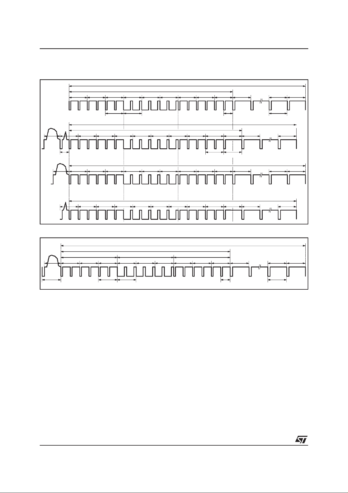
Figure2 : PAL-BDGHI,PAL-N TypicalVBI Waveform,InterlacedMode (CCIR-625 Line Numbering)
0
V
IV
308 309 310 311 312 313 314 315 316 317 318 319 320
PartialVBI1
624 625 1 2 3 4 5 6 7 23621 622 623
Partial VBI2
Full VBI1
I
Full VBI2
A
II
AB
A
22
E
A
V
0119A-08.EPS
335
C
:
0
V
I, II, III, IV :
A:
B:
C:
311 312 313 314 315 316 317 318 317 336308 309 310
62462512345678621 622 623
Frame synchronizationreference
st
1
and 5th,2ndand6th,3rdand 7th,4thand 8thfields
Burst phase : nominal value +135°
Burst phase : nominal value -135°
Burst suppressioninternal
III
AB
I
II
III
IV
Figure3 : PAL-BDGHI,PAL-NTypicalVBI Waveform,Non-interlaced Mode (“CCIR-like” LineNumbering)
Full VBI
AB
22
7/42
Burst phase toggles every line
0
V
31131212345678308 309 310
PartialVBI
0119A-09.EPS
0119A-10.EPS
Page 8
STV0119A
IV- FUNCTIONAL DESCRIPTION(continued)
Figure4 : NTSC-MTypical VBI Waveforms,InterlacedMode (SMPTE-525Line Numbering)
1
23
Partial VBI1
45678910 1819
Full VBI1
Partial VBI2
Full VBI2
HH0.5H
VBI3
12345678910 1819525
VBI4
H0.5HHH
282273272271270269268267266265264263262
282273272271270269268267266265264263
Figure5 : NTSC-MTypical VBI Waveforms,Non-interlacedMode (“SMPTE-like” Line Numbering)
Full VBI
PartialVBI
262
1
H
233H4563H7893H10 18 19
H0.5HHH
0119A-11.EPS
0119A-12.EPS
8/42
Page 9
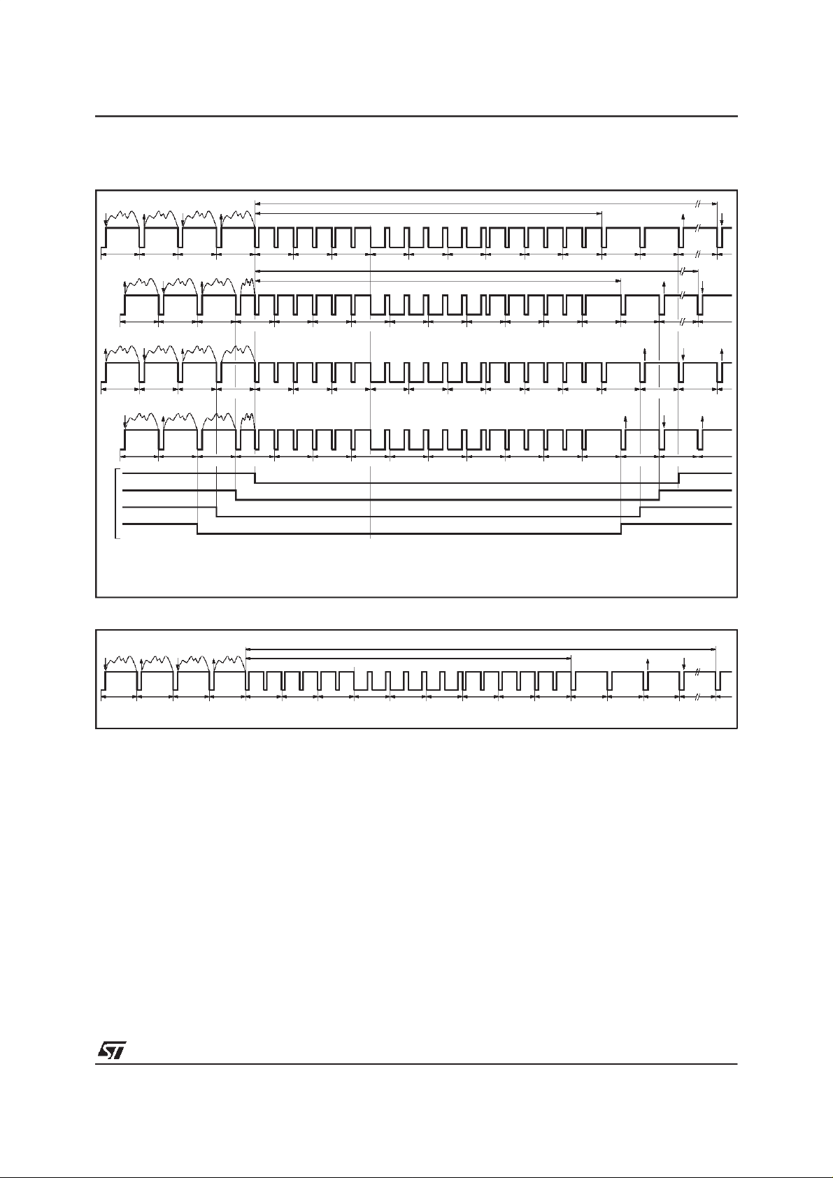
IV- FUNCTIONAL DESCRIPTION(continued)
Figure6 : PAL-MTypical VBI Waveforms,InterlacedMode (CCIR-525 Line Numbering)
F’
0
PartialVBI1
V
I
FullVBI1
STV0119A
AB
519F520F’521F522 523 524 525 1 2 3 4 5 6 7 8 9
F
257F’258F259 260
F
519F’520F521 522
F’
257F258 259 260
C
0V:
Framesynchronizationreference
I, II, III, IV :
1stand5th,2ndand6th,3rdand7th,4thand8thfields
A:
Burstphase: nominalvalue +135°
B:
Burstphase: nominalvalue -135°
C:
Burstsuppressioninternal
261 262 263 264 265 266 267 268 269 270 271 280
523 524 525 1 2 3 4 5 6 7 8 9
261 262 263 264 265 266 267 268 269 270 271 272
PartialVBI2
II
III
IV
I
II
III
IV
FullVBI2
AB
AB
Figure7 : PAL-MTypical VBI Waveforms,Non-interlacedMode(“CCIR-like” Line Numbering)
0
V
Partial VBI
Full VBI
AB
16 17
AB
279
0119A-13.EPS
256257258259260261262123456789
Burstphase toggles every line
10 16 17
0119A-14.EPS
9/42
Page 10
STV0119A
IV- FUNCTIONAL DESCRIPTION(continued)
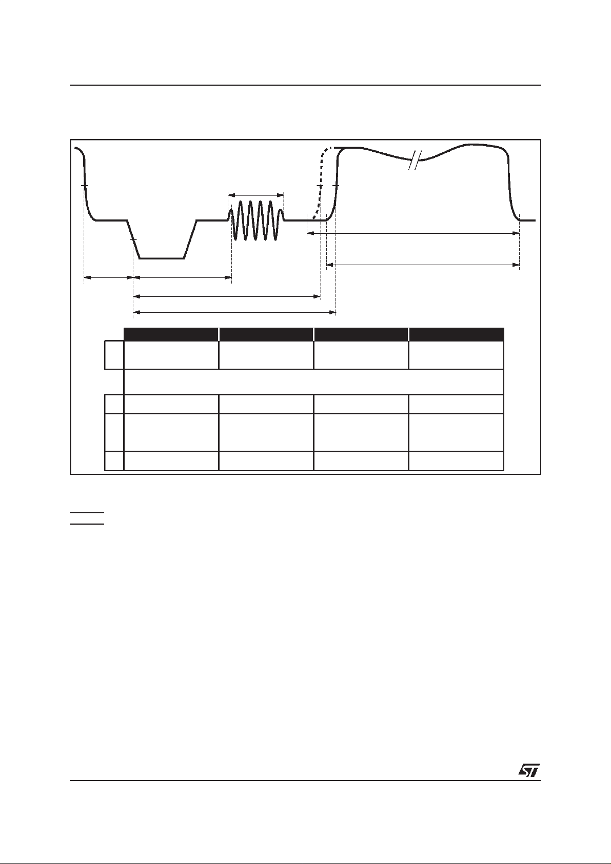
Figure8 : Horizontal Blanking Intervaland Active VideoTimings
d
0
H
b
a
(bit”aline” = 0)
c1
c2 (bit ”aline” =1)
Full Digital Line Encoding
(720Pixels - 1440T)
”Analog” Line Encoding
(710Pixels - 1420T)
NTSC-M
5.38µs(even lines)
a
5.52µs(odd lines)
Actual values will depend on the static offset programmed for subcarrier generation.
b
c1
c2
d
1.56µs
8.8µs
9.3µs
9 Cycles of 3.58MHz
PAL-BDGHI
5.54µs(A-type)
5.66µs(B-type)
Theseare typical values.
1.28µs
9.3µs
10.1µs
10 Cyclesof 4.43MHz
IV.3 - Reset Procedure
Ahardwareresetis performedbygroundingthe Pin
RESET. Themasterclockmustberunningand Pin
RESET kept low for a minimum of 5 clockcycles.
This sets the STV0119A in HSYNC+ODDEVEN
(line-locked) slave mode, for NTSC-M, interlaced
ITU-R601encoding with Macrovision
TM
copyprotection revision 7.01 operating. Closed-captioning
and Teletextencodingare all disabled.
Then the configuration can be customizedby writing into the appropriate registers. A few registers
PAL-N
5.54µs(A-type)
5.66µs(B-type)
1.28µs
9.3µs
10.1µs
9 Cycles of 3.58MHz
PAL-M
5.73µs(A-type)
5.87µs(B-type)
1.28µs
9.3µs
10.1µs
9 Cycles of 3.58MHz
are never reset,their contentsis unknownuntilthe
first loading (refer to the Register Contents and
Description).
It is also possible to perform a software reset by
settingbit’softreset’in Reg6. The IC’sresponsein
that caseis similarto itsresponseaftera hardware
reset, except that Configuration Registers
(Reg0 to6) anda few otherregisters(seedescription of bit‘softreset’)are not altered.
0119A-15.EPS
10/42
Page 11
STV0119A
IV- FUNCTIONAL DESCRIPTION(continued)
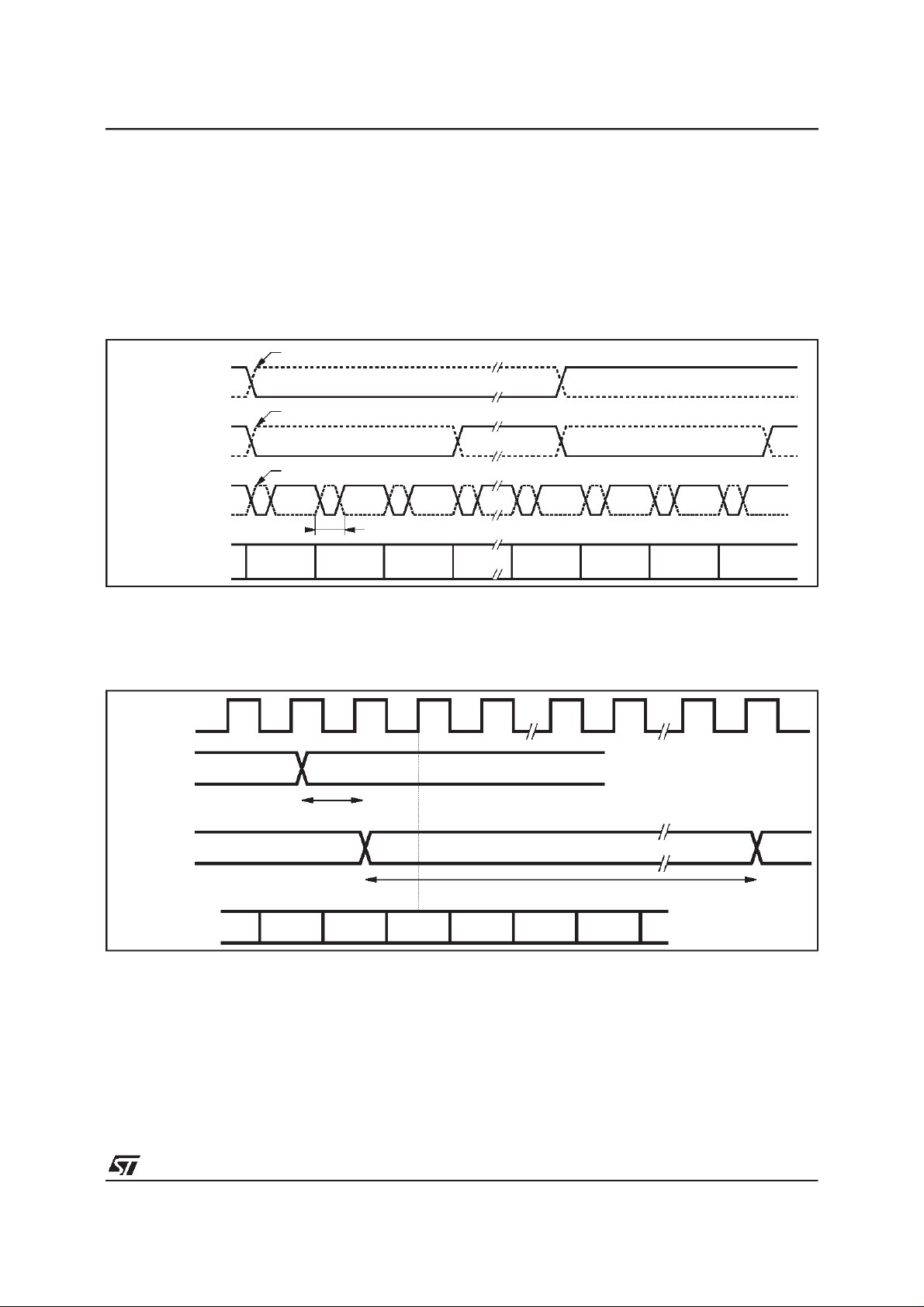
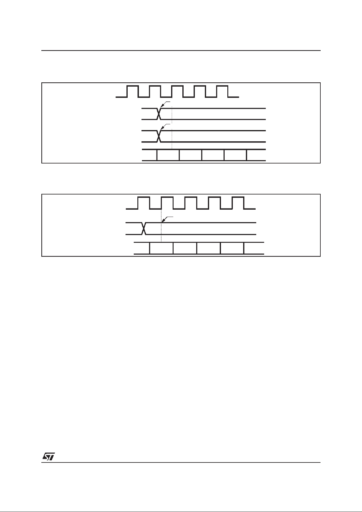
IV.4 - MasterMode
In this mode, the STV0119Asupplies HSYNC and
ODDEVEN sync signals (with independentlyprogrammablepolarities) to drive other blocks. Refer
to Figure9 and 10 for timings and waveforms.
TheSTV0119Astartsencodingand countingclock
Figure9 : ODDEVEN,VSYNC and HSYNC Waveforms
Active edge (programmable polarity)
ODDEVEN
(see Note 1)
Active edge (programmable polarity)
VSYNC
Active edge (programmable polarity)
HSYNC
(see Note 2)
Line Numbers :
SMPTE-525
CCIR-62541
Notes : 1. When ODDEVEN is a sync input, only one edge (“the active edge”) of the incoming ODDEVEN is taken into account for
synchronization. The “non-active” edge (2nd edge on thisdrawing) is not critical andits position may differ by H/2 from the location
shown.
2. The HSYNC pulse width indicated is valid when the STV0119Asupplies HSYNC.In those slave modes where it receives HSYNC,
only the edge defined as activeis relevant,and thewidthof the HSYNC pulse it receives is not critical.
128 T
5
2
6
3
ckref
= 4.74µs
cycles as soon as the master mode has been
loadedinto thecontrol register(Reg.0).
Configuration bits ”Syncout_ad[1:0]”(Reg4) allow
toshiftthe relativepositionofthesyncsignalsbyup
to 3 clockcyclesto copewith anyYCrCb phasing.
266
313
267
314
268
315
269
316
0119A-16.EPS
Figure10 : MasterMode Sync Signals
CKREF
ODDEVEN
(out)
HSYNC
(out)
YCRCB
Note : 1. This figureis valid for bits “syncout_ad[1:0]” = default.
Active Edge
(programmable polarity)
1T
CKREF
Cr Y’
Active Edge
(programmable polarity)
Cb Y Cr Y’
Duration of HSYNC Pulse : 128T
CKREF
0119A-17.EPS
11/42
Page 12

STV0119A
IV- FUNCTIONAL DESCRIPTION(continued)
IV.5 - SlaveModes
Sixslavemodesareavailable:ODDEVEN+HSYNC
based (line-based sync), VSYNC+HSYNC based
(anothertype of line-basedsync),ODDEVEN-only
based(frame-basedsync),VSYNC-onlybased(another type of frame-based sync), or sync-in-data
based(line lockedor framelocked).
ODDEVEN refers to an odd/even (also known as
not-top/bottom) field flag, HSYNC is a line sync
signal,VSYNCis a verticalsyncsignal.Theirwaveforms are depicted in Figure 9. The polarities of
HSYNC and VSYNC/ODDEVEN a re independentlyprogrammablein all slave modes.
IV.5.1- Synchronizationontoa LineSyncSignal
IV.5.1.1- HSYNC+ODDEVENBased
Synchronization
Synchronizationis performedon a line-by-line basis by locking onto incoming ODDEVEN and
HSYNCsignals. Refer to Figure 11for waveforms
and timings. The polarities of the active edges of
HSYNC and ODDEVEN are programmable and
independent.
The first active edge of ODDEVEN initializes the
internal line counter but encoding of the first line
does not start until an HSYNC active edge is detected(at theearliest,HSYNCmaytransitionat the
sametimeas ODDEENV).Atthatpoint,the internal
sample counter is initialized and encoding of the
firstlinestarts.Then,encodingof eachsubsequent
line is individually triggered by HSYNC active
edges. The phase relationship between HSYNC
andthe incomingYCrCB data isnormallysuchthat
the first clock rising edge following the HSYNC
active edge samples ”Cb” (i.e. a ‘blue’ chroma
sample within the YCrCb stream). It is however
possibleto internallydelay the incoming sync signals (HSYNC+ODDEVEN) by up to 3 clockcycles
to cope with different data/sync phasings, using
Figure11 : HSYNC+ ODDEVENBased Slave Mode Sync Signals
configurationbits ”Syncin_ad”(Reg. 4).
The STV0119Ais thus fully slaved to the HSYNC
signal, which means that lines may contain more
or less samples than typical 525/625 system requirement.
If the digital line is shorter than its nominal value:
the samplecounterisre-initializedwhenthe ‘early’
HSYNC arrives and all internal synchronization
signals are re-initialized.
If the digital line is longer than its nominal value :
the sample counter is stoppedwhen it reachesits
nominal end-of-line value and waits for the ‘late’
HSYNCbefore reinitializing.
ThefieldcounterisincrementedoneachODDEVEN
transition. The line counteris reset on the HSYNC
followingeachactiveedgeof ODDEVEN.
IV.5.1.2- HSYNC + VSYNC Based Synchronization
Synchronizationis performed on a line-by-linebasis by locking onto incoming VSYNC and HSYNC
signals. Refer to Figure 12 for waveforms and
timings. The polaritiesof HSYNC and VSYNC are
programmableand independent.
The incomingVSYNC signal is immediately transformed into a waveform identical to the odd/even
waveform of an ODDEVEN signal, therefore the
behavior of the core is identical to that described
aboveforODDEVEN+HSYNCbased synchronization. Again, the p hase relationship between
HSYNC and the incoming YCrCb data is normally
such that the first clock rising edge following the
HSYNC active edge samples ”Cb” (i.e. a ‘blue’
chroma sample within the YCrCb stream). It is
however possible to internally delay the incoming
sync signals (HSYNC+VSYNC) by up to 3 clock
cycles to cope with different data/sync phasings,
using configurationbits ”Syncin_ad” (Reg.4).
The field counter is incremented on each active
edge of VSYNC.
CKREF
ActiveEdge (programmablepolarity)
ODDEVEN
(in)
HSYNC
(in)
YCRCB
Note : 1. This figure is valid for bits “syncin_ad[1:0]” = default.
12/42
ActiveEdge (programmablepolarity)
Cb Y Cr Y’ Cb
0119A-18.EPS
Page 13
IV- FUNCTIONAL DESCRIPTION(continued)
Figure12 : HSYNC+ VSYNC Based Slave Mode Sync Signals
CKREF
Active Edge (programmablepolarity)
VSYNC
(in)
Active Edge (programmablepolarity)
HSYNC
(in)
STV0119A
YCRCB Cb Y Cr Y’ Cb
Notes : 1. This figure is valid for bits “syncin_ad[1:0]” = default.
2. The active edges of HSYNC and VSYNC should normally be simultaneous. It is permissible that HSYNC transitions before
VSYNC, but VSYNC must not transition before HSYNC.
Figure13 : ODDEVENBased Slave Mode Sync Signals
CKREF
Active Edge (programmable polarity)
ODDEVEN
(in)
YCRCB
Note : 1. This figure is valid for bits “syncin_ad[1:0]” = default.
IV .5 .2-Synchro niza t ionontoa FrameSyncSignal
IV .5.2.1- ODDEVEN- onl yBasedSynchronizati on
Synchronizationis performedona frame-by-frame
basisby lockingonto an incoming ODDEVEN signal. A line sync signal is derived internally and is
also output as HSYNC. Refer to Figure 13 for
waveforms and timings. The phase relationship
betweenODDEVENand the incomingYCrCB data
is normally such that the first clock rising edge
followingthe ODDEVENactiveedge samples”Cb”
(i.e. a ‘blue’ chroma sample within the YCrCb
stream). It is however possible to internally delay
the incoming ODDEVEN signal by up to 3 clock
cycles to cope with different data/sync phasings,
using configurationbits ”Syncin_ad”(Reg. 4).
Thefirstactiveedgeof ODDEVENtriggersgenerationofthe analogsyncsignalsand encodingof the
incomingvideo data.Framesbeingsupposedtobe
of constant duration, the next ODDEVEN active
transitionisexpectedat aprecisetimeafterthelast
ODDEVENdetected.
So, once an active ODDEVEN edge has been
detected,checks that the followingODDEVENare
presentat the expected instantsare performed.
Encodingandanalog sync generationcarry on un-
Cb Y Cr Y’ Cb
less three successive fails of these checks occur.
In that case,three behaviorsare possible,accord-
ing to the configurationprogrammed(Reg. 1-2) :
- if ‘free-run’is enabled, the STV0119A carries on
outputtingthe digitalline syncHSYNCand generating analog video just as though the expected
ODDEVEN edge had been present. However, it
willre-synchronizeontothenextODDEVENactive
edgedetected,whateverits location.
- if ‘free-run’ is disabled but bit ‘sync_ok’ is set in
configuration register1, the STV0119A sets the
active portion of the TV line to black level but
carrieson outputtingthe analog sync tips (on Ys
and CVBS) and the digital line sync signal
HSYNC. (When programmed, Macrovision
pseudo-sync pulses and AGC pulses are also
presentin the analog syncwaveform).
- if ‘free-run’is disabledand the bit‘sync_ok’is not
set, allanalog video is at blacklevel and neither
analog sync tips nor digital line sync are output.
Note that this mode is a frame-basedsync mode,
asopposedtoa field-basedsyncmode,thatis,only
one type of edge (rising or falling,according to bit
‘polv’in Reg 0) is of interest to the STV0119A,the
other one is ignored.
0119A-19.EPS
0119A-20.EPS
TM
13/42
Page 14

STV0119A
IV- FUNCTIONAL DESCRIPTION(continued)
IV.5.2.2- VSYNC only Based Synchronization
Synchronizationis performed on a frame-by-frame
basis by locking onto an incoming VSYNC signal.
An auxiliary line sync signal HSYNC must also be
fed to the STV0119A,which uses it to reconstruct
from VSYNC and HSYNC information an internal
odd/even waveform identical to that of an ODDEVENsignal.Thereforethe behaviorof thecore is
identicaltothatdescribedaboveforODDEVENonly
basedsynchronization(exceptthatnothingisoutput
onHSYNCpin sinceit isan inputportin thatmode).
Notethat HSYNC is an input buthas no other use
thanallowing the STV0119Ato decide whether an
incoming VSYNC pulse flags an odd or an even
field. In other words, the STV0119Adoes not lock
onto HSYNC in this mode since this is NOT a
line-locked mode.
The phase relationship between VSYNC and the
incomingYCrCb data is normallysuch that the first
clockrising edgefollowingthe VSYNC activeedge
samples ”Cb” (i.e. a ‘blue’ chroma sample within
theYCrCb stream). It is howeverpossibleto internally delay the incoming sync signals
(VSYNC+HSYNC)by up to 3 clock cycles to cope
withdifferentdata/syncphasings,using configurationbits ”Syncin_ad”(Reg. 4).
IV.5.3- Synchronizationonto Data-embedded
SyncWords
IV.5.3.1- ‘End-of-frame’Word Based
Synchronization
Synchronizationis performed by extracting the 1to-0 transitions of the ‘F’ flag (end-of-frame) from
the ‘EAV’(End-of-ActiveVideo) sequenceembedded within ITU-R656 / D1 compliant digital video
streams.Both a framesync signal and a line sync
signal are derived and are made available externally as ODDEVEN and HSYNC (see Figure14).
Thefirstsuccessfuldetectionof the‘F’flagtriggers
generationof theanalogsyncsignalsandencoding
of the incoming video data. Frames being supposed to be of constant duration, the next EAV
wordcontainingthe ‘F’flagis expectedat a precise
time after the latest detection.
Figure14 : Data(EAV)Based Slave Mode Sync Signals
So, once an active ‘F’ flag has been detected,
checks that the following flags are present within
the incoming video stream at the expected times
are performed.
Encodingand analogsync generationcarry on unlessthreesuccessivefailsof thesechecks occur.
In that case, three behaviors are possible, according to the configurationprogrammed :
- if ‘free-run’is enabled, the STV0119Acarries on
- if ‘free-run’is disabledbut the bit‘sync_ok’is setin
- if ‘free-run’isdisabledandthebit‘sync_ok ’isnotset,
The SAV and EAVwords are Hamming-decoded.
Afterdetectionof two successiveerrors, abit is set
in the statusregister to informthe micro-controller
of thepoor transmissionquality.
IV.5.3.2- ‘End-of-line’Word Based
Synchronizationis performed by extracting the ‘F’
and ‘H’ flags from the ‘SAV’(Start of Active Video)
and ‘EAV’(End of Active Video) words embedded
withinITU-R656/D1compliantdigitalvideostreams.
Alinesyncsignalandaframesyncsignalarederived
internally from these flags and are output on the
HSYNC and ODDEVEN/VSYNC pins in output
mode.These signalsare also exploitedby thecore
ofthecircuitwhichtreatsthem likeittreatsincoming
ODDEVENandHSYNC signalsin HSYNC+ODDEVENbasedsynchronization(see SectionIV.5.1.1).
generatingthedigital frameandlinesyncs(ODDEVENand HSYNC)and generatinganalogvideo
just as though the expected ‘F’ flag had been
present. However, it will re-synchronize onto the
ne xt ‘F’ flag dete cte d within the incoming
CCIR656/D1 video stream.
the configuration registers, the STV0119Asetsthe
activeportionoftheTVline toblacklevelbutcarries
onoutputtingtheanalogsynctips(onYsandCVBS)
andthedigitalfram eandlinesyncsignalsODDEVEN
and HSYNC. (When program m ed, Macrov i s i o n
pseudo-syncpulsesand AGC pulsesare also presentintheanalogsyncwaveform).
all analogvideo is at blackleveland neitheranalog
synctipsnordigitalframe/linesyncareoutput.
Synchronization
14/42
CKREF
YCRCB
ODDEVEN
(out)
HSYNC
(out)
FF 00
00 B6 Cb Y
EAV
46T
CKREF
HSYNCDuration : 128T
1T
CKREF
CKREF
0119A-21.EPS
Page 15

IV- FUNCTIONAL DESCRIPTION(continued)
IV.6 - Input Demultiplexer
The incoming 27Mbit/s YCrCb data is demultiplexed into a ‘blue-difference’chroma information
stream, a ‘red-difference’ chroma information
stream and a luma information stream. Incoming
databits are treated as blue, red or lumasamples
according to their relative position with respect to
the sync signals in use and to the content of configurationbits ”Syncin_ad” (slave modes) or ”Syncout_ad”(master mode).
The ITU-R601 recommendationdefines the black
luma level as Y = 16dec and the maximum white
luma level as Y = 235dec. Similarly it defines 225
quantizationlevels for thecolor differencecomponents(Cr, Cb), centered around 128.
Accordingly, incoming YCrCB samples can be
saturatedin the inputmultiplexerwiththe following
rules :
- for Cr or Cb samples :
Cr,Cb > 240 ⇒ Cr,Cb saturatedat 240
Cr,Cb< 16⇒Cr,Cb saturated at 16
- for Y samples:
Y > 235 ⇒ Ysaturatedat 235
Y<16⇒Ysaturatedat 16
This avoids having to heavily saturate the composite video codes before digital-to-analog conversion in case erroneous or unrealistic YCrCb
samples are input to the encoder (there may
otherwise be overflow errors in the codes driving
the DACs), and therefore avoids genera-ting a
distorded output waveform.
However,in someapplications,it maybe desirable
to let ‘extreme’ YCrCb codes pass through the
demultiplexer. This is also possible, provided that
bit ”maxdyn” is setin configuationregister 6.
In this case, only codes 00hex and FFhex are
overridden: if such codes are found in the active
video samples, they are forced to 01hex and FEhex.
In any case, the YCrCb codes are not overridden
for EAV/SAVdecoding
The demultiplexer is also able to handle 54Mbit/s
STV0119A
YCrCbstreamsfordualencodingapplications.Refer to Section IV.17,”Dual Encoding Application 54Mbit/s YCrCB interface”.
IV.7- Sub-carrierGeneration
A Direct Digital Frequency Synthesizer (DDFS)
using a 24-bit phase accumulator, generates the
requiredcolorsub-carrierfrequency.Thisoscillator
feedsaquadraturemodulatorwhichmodulatesthe
basebandchrominancecomponents.
The sub-carrier frequency is obtained from the
followingequation :
Fsc = (24-bit Increment Word / 2
Hard-wired Increment Word values are available
foreachstandard(exceptfor ‘NTSC-4.43’)andcan
be automaticallyselected.Alternatively(according
to bit ‘selrst’ in Reg.2.), thefrequencycan be fully
customized by programming other values into a
dedicated Increment Word Register (Reg. 10-11-
12). This allows for instance to encode ”NTSC-
4.43” or ”PAL-M-4.43”.
This is done with the followingprocedure :
- Program the required increment in Registers 10
to12
- Set bit ‘selrst’ to ‘1’in ConfigurationRegister2
- Perform a softwarereset (Reg. 6).
Caution : this sets back all bits from Reg. 7
onwardsto theirdefault value, when theycan be
reset.
Warning :
if a standard change occurs after the
softwarereset,theincrementvalueisautomatically
re-initialized with the hardwired or loaded value
accordingto bit selrst.
The reset phase of the color sub-carrier can also
be software-controlled(Reg. 13-14).
The sub-carrier phasecan be periodically reset to
its nominal value to compensatefor any drift introduced by the finite accuracy of the calculations.
Sub-carrier phase adjustment can be performed
every line, every eight field, every four field, or
every two field (Register2 bits valrst[1:0]).
24
) x CKREF
15/42
Page 16

STV0119A
IV- FUNCTIONAL DESCRIPTION(continued)
IV.8 - BurstInsertion
The color reference burst is inserted so as to
always start with a positive zero crossing of the
subcarriersine wave (exceptinsome caseswhere
Macrovisionanti-copyprocessis active).Thefirst
and last half-cycles have a reduced amplitude so
that the burst envelope startsand ends smoothly.
The burst contains 9 or 10 sine cycles of
4.43361875MHzor3.579545MHzaccordingto the
standard programmed in the Control Register
(Reg. 0, bits std[1:0]), as follows:
- NTSC-M 9 cyclesof 3.579542MHz
- PAL-BDGHI 10 cycles of 4.43361875MHz
- PAL-M 9 cycles of 3.57561149MHz
- PAL-N 9 cyclesof 3.5820558MHz
Itis possibleto turn theburstoff(noburstinsertion)
bysettingconfigurationbit ‘bursten’to0(register2).
Notes :
- Two strategies exist for burst insertion: one is to merely
gateand shapethe subcarrierforburstinsertion,theother
is more elaborated and is to always start the burst with a
positive-going zero crossing. In the first case the phase
of the subcarrier when the burst starts is not controlled,
with theconsequence that some ofits firstand last cycles
are more heavily distorded. T he second so lut ion
guaranteessmoothstartand endof burstwitha maximum
of undistorded burst cycles and can only be beneficial to
chroma decoders, it is the solution implemented in the
STV0119A.
- While the first option gave constant burst start time but
uncontrolled initial burst phase, the second solution
guarantees start on a positive-going zero crossing with
the consequence that two burst start locations are visible
over successive lines, accordingto the line parity.This is
normal and explained below.
- In NTSC, the relation between subcarrier frequency and
line length creates a 180o subcarrier phase difference
(with respect to the horizontal sync) from one line to the
next according to the line parity. So if the burst always
startswith thesame phase(positive-goingzero crossing),
this means the burst will be inserted at time X or at time
/2 after the horizontal sync tip according to the
X+T
NTSC
line parity,where T
NTSC burst.
- With PAL, a similar rationale holds, and again there will
be two possible burst start locations. The subcarrier
phasedifference (withrespecttothehorizontal sync)from
one line to the next in that case is either 0 or 180o with
the following series: A-A-B-B-A-A-...-etc. where A
denotes ‘A-type’ bursts and B denotes ‘B-type’ bursts,
A-type and B-type being 180° out of phase with respect
to the horizontal sync. So 2 locations are possible, one
for A-type,the other forB-type (see Figure8).
- This assumes a periodic reset of the subcarrier is
automatically performed (see bits valrst[1:0] in Reg 2).
Otherwise, over severalframes, the start ofburst will drift
within an interval of one a subcarrier’s cycle. THIS IS
NORMAL and means the burst is correctly locked to the
colors encoded. The equivalent effect witha gated burst
approachwould be thefollowing : the start locationwould
be fixed but the phase with which the burst starts (with
respect to the horizontal sync) would be drifting.
IV.9 - LuminanceEncoding
ThedemultiplexedYsamplesare band-limitedand
interpolated at CKREF clock rate. The resulting
luminancesignalis properlyscaledbeforeinsertion
of any Closed-captions, CGMS or Teletext data,
Macrovision
16/42
TM
copy-protection signals and syn-
is the duration ofone cycle of the
NTSC
chronizationpulses.
Theinterpolationfiltercompensatesforthesin(x)/x
attenuationinherent to D/Aconversion and greatly
simplifiesthe outputstagefilter(referto Figures15
to17 for characteristiccurves).
Figure 15 : LumaFiltering IncludingDAC
Attenuation
0
-5
-10
-15
-20
-25
-30
Amplitude (dB)
-35
-40
01234567 9108111213
6
Frequency (x10
) (Hz)
Figure 16 : LumaFiltering with 3.58MHz Trap,
IncludingDAC Attenuation
0
-5
-10
-15
-20
-25
-30
Amplitude (dB)
-35
-40
01234567 9108 111213
6
Frequency (x10
) (Hz)
Figure 17 : LumaFiltering with 4.43MHz Trap,
IncludingDAC Attenuation
0
-5
-10
-15
-20
-25
-30
Amplitude (dB)
-35
-40
01234567 9108 111213
Frequency (x10
6
) (Hz)
0119A-22.EPS
0119A-23.EPS
0119A-24.EPS
Page 17

IV- FUNCTIONAL DESCRIPTION(continued)
In addition, the luminance that is added to the
chrominanceto createthe compositeCVBS signal
can be trap-filtered at 3.58MHz (NTSC) o r
4.43MHz (PAL). This allows to cope with application oriented towards low-end TV sets which are
subject to cross-color if the digital source has a
wide luminance band width (e.g. some DVD
sources).Notethat thetrapfilterdoesnotaffect the
S-VHSluminance output nor the RGB outputs.
A7.5 IRE pedestalcan be programmed if needed
withall standards(seeReg1,bit setup).Thisallows
in particular to encode Argentinian and non-Argentinian PAL-N, or JapaneseNTSC (NTSC with
no set-up).
A programmable delay can be inserted on the
luminance path to compensate any chroma/luma
delay introduced by off-chip filtering (chroma and
lumatransitionsbeingcoincidentat theDACoutput
withdefault delay) (Reg3, bits del[2:0]).
IV.10- Chrominance Encoding
U and V chroma components are computed from
demultiplexedCb, Cr samples.Before modulating
thesubcarrier,theseare band-limitedand interpolated at CKREFclock rate. This processing eases
the filtering following D/Aconversion and allows a
more accurate encoding.A set of 4 differentfilters
is availablefor chroma filtering to fit a wide variety
of applications in the different standards and includefiltersrecommendedbyITU-RRec624-4and
SMPTE170-M.The available 3dB bandwidthsare
1.1, 1.3, 1.6 or 1.9MHz, refer to Figures 18 to 22
for the various frequency responses (Reg1, bits
flt[1:0]).
Thenarrowerbandwidthsareusefulagainstcrossluminanceartefacts,the widerbandwidthsallow to
keep higher chroma contents and then an improvedimage quality.
IV.11- Composite Video Signal Generation
The composite video signal is created by adding
the luminance (after optional trap filtering, Reg 3
bits entrap and trap_pal) and the chrominance
components.Asaturationfunctionis includedinthe
adder to avoid overflow errors should extreme
luminance levels be modulated with highly saturated colors (this does not correspond to natural
colors but may be generated by computers or
graphicengines).
A‘colorkilling’functionis available(Reg1,bit coki)
wherebythe compositesignal containsno chrominance, i.e. replicates the trap-filtered luminance.
STV0119A
Note that this function does not suppress the
chrominanceon the S-VHSoutputs (nevertheless
suppressing the S-VHS chrominance is possible
using bit ”bkg_c”in Reg 5).
Figure 18 : VariousChroma FiltersAvailable
+ RGB Filter
1
0
-1
-2
-3
-4
-5
-6
Amplitude(dB)
-7
-8
-9
0 0.5 1.5 21 2.5 3 3.5
f
=1.1
3
Frequency(x106) (Hz)
f
=1.3
3
Figure 19 : 1.1MHzChromaFilter (flt = 00)
0
-5
-10
-15
-20
-25
Amplitude (dB)
-30
-35
-40
0 2 4 6 8 10 12 14
Frequency (x10
Figure 20 : 1.3MHzChromaFilter (flt = 01)
0
-5
-10
-15
-20
-25
Amplitude (dB)
-30
-35
-40
0 2 4 6 8 10 12 14
Frequency(x10
f3=1.6
6
) (Hz)
6
) (Hz)
RGB
f3=1.9
f
=2.45
3
0119A-25.EPS
0119A-26.EPS
0119A-27EPS
17/42
Page 18

STV0119A
IV- FUNCTIONAL DESCRIPTION(continued)
Figure21 : 1.6MHzChroma Filter (flt = 10)
0
-5
-10
-15
-20
-25
Amplitude (dB)
-30
-35
-40
0 2 4 6 8 10 12 14
Frequency(x10
Figure22 : 1.9MHzChroma Filter (flt = 11)
0
-5
-10
-15
-20
-25
Amplitude (dB)
-30
-35
-40
0 2 4 6 8 101214
Frequency(x10
IV.12- RGBEncoding
After demultiplexing, the Cr and Cb samples feed
a 4 times interpolation filter. The resulting baseband chroma signal has a 2.45MHz bandwidth
(Figure 23) and is combinedwith the filtered luma
componenttogenerateR, G, B samplesat 27MHz.
Figure23 : RGBChroma Filtering
0
-5
-10
-15
-20
-25
Amplitude (dB)
-30
-35
-40
0 2 4 6 8 101214
Frequency(x10
6
) (Hz)
6
) (Hz)
6
) (Hz)
IV.13- ClosedCaptioning
Closed-captions(or data from an Extended Data
Serviceas defined by the Closed-Captionsspecification)can be encoded by thecircuit.The closed
caption data is delivered to the circuit through the
2
I
C interface. Two dedicated pairs of bytes (two
bytes per field), each pair preceded by a clock
run-in and a start bit canbe encodedand inserted
on the luminancepath on a selected TV line. The
ClockRun-In and Start code are generatedby the
STV0119A.
Closed-captiondata registersare double-buffered
so that loading can be performed anytime, even
duringline 21/284 or any otherselected line.
0119A-28.EPS
Userregister39(resp.41) containsthe firstbyteto
send(LSBfirst)after thestartbit on the appropriate
TVline in field1 (resp.field 2),anduserregister40
(resp. 42) contains the second byte to send. The
TV line number where data is to be encoded is
programmble (Reg. 37, 38). Lines that may be
selectedinclude those usedby the StarSightdata
broadcastsystem.Closed-captionsdata haspriorityoveranyCGMSor Macrovisionanticopysignals
programmedfor the same line.
Theinternal Clock Run-In generator is based on a
DirectDigital FrequencySynthesizer.The nominal
instantaneousdatarate is 503.5kbit/s(i.e.32times
theNTSC line rate). Data LOW correspondsnominallyto 0 IRE,data HIGH correspondsto 50 IREat
the DAC outputs. Refer to Figure 24.
0119A-29.EPS
When closed-captioning is on (bits cc1/cc2 in
Reg.1),the CPU should load the relevantregisters
(reg.39 and40, or 41 and 42) once everyframe at
most(althoughthere is in factsome margindue to
thedouble-buffering).Twobits are setin thestatus
registerin case of attemptsto loadthe closed-caption data registers too frequently, these can be
used to regulateloading rate.
Figure 24 : ExampleClosed-captionWaveform
300
250
200
150
LSB
100
50
0119A-30.EPS
0
10µs
27.35µs
13.9µs
7 cycles
of 504kHz
Transition
Time : 220ns
61µs
t
0119A-31.EPS
18/42
Page 19

IV- FUNCTIONAL DESCRIPTION(continued)
The closed caption encoderconsiders that closed
caption data has been loaded and is valid on
completion of the write operation into register 40
forfield1,intoregister42forfield2.Ifclosedcaption
encodinghasbeenenabledandnonew databytes
have been written into the closed caption data
registerswhentheclosedcaptionwindowstartson
theappropriateTV line,then thecircuitoutputstwo
US-ASCIINULLcharacterswithoddparityafterthe
start bit.
IV.14- CGMSEncoding
CGMS (Copy Generation Management System also known as VBID and described by standard
CPX-1204 of EIAJ) data can be encoded by the
circuit. Three bytes (20 significant bits) are deliveredto thechipviathe I
2
Cinterface.Tworeference
bits (‘1’ then ‘0’) are encoded first, followed by 20
bitsof CGMSdata (includinga CyclicRedundancy
Checksequence,not computedby the deviceand
supplied to it as part of the 20 data bits). The
reference bits are generated locally by the
STV0119A.Refer to Figure 25 for a typicalCGMS
waveform.
WhenCGMS encodingisenabled,theCGMS(see
bit encgms in Reg 3) waveform is continously
present once in each field, on lines 20 and 283
(SMPTE-525line numbering).CGMSdatahas priority over any Macrovision anticopy signals programmedfor the same line.
TheCGMSdata registeris double-buffered,which
meansthatit can be loadedanytime (even during
line 20/283) without any risk of corrupting CGMS
data that could be in the process of being encoded.The CGMS encoder considers that new
CGMSdata has been loaded and is valid on completionof the writeoperation into register 33
Figure25 : ExampleCGMSWaveform
300
250
200
150
LSB
100
50
0
11µs
Word 0
6 bits
Bit 1 Bit 20
t
48.7µs
Word 1
4 bits
Word 2
4 bits
CRCC
6 bits
STV0119A
IV.15- TeletextEncoding
The STV0119Ais able to encode Teletext accordingto the ”CCIR/ITU-R BroadcastTeletextSystem
B” specification, also known as ”World System
Teletext”.
In DVB applications, Teletext data is embedded
within DVB streams as MPEG data packets. It is
theresponsibilityofa ”TransportLayerProcessing”
IC (or demultiplexer),like ST’s ST20-based”TP2”,
to sort out incomingdata packetsand in particular
to store Teletext packet in a buffer, which then
passes them to the STV0119Aon request.
IV.15.1- Signals Exchanged
TheSTV0119Aand the Teletextbufferexchange2
signals: TTXS (Teletext Synchronization) going
fromtheSTV0119Ato theTeletextBufferandTTXD
(TeletextData)goingfromtheTeletextBuffertothe
STV0119A.
The TTXS signal is a request signal generated on
selected lines. In response to this signal, the
Teletextbufferisexpectedto send360Teletextbits
tothe STV0119Afor insertionof a Teletextline into
the analog video signal.
Thedurationof theTTXSwindowis 1402reference
clockperiods(51.926µs),whichcorrespondsto the
duration of 360 Teletext bits (see Transmission
Protocolbelow).
Following the TTXS rising edge the encoder expectsdata fromtheTeletextbufferaftera programmable number (2 to 9) of 27MHz master clock
periods.Dataistransmittedsynchronouslywiththe
master clock at an average rate of 6.9375Mbit/s
accordingto the protocol described below. It consists, in order of transmission, of 16 Clock Run-In
bits, 8 Framing Code bits and the 336 bits
(42 bytes) that represent one Teletextpacket.
IV.15.2- TransmissionProtocol
In order to transmit the Teletext data bits at an
average rate of 6.9375Mbit/s, which is about
1/3.89 times the masterclock frequency,the followingscheme is adopted:
The 360-bit packet is regarded as nine 37-bit sequences plus one 27-bit sequence. In every sequence, each Teletext data bit is transmittedas a
successionof4identicalsamplesat27Msample/s,
exceptfor the 10th, 19th, 28th and 37th bitsof the
sequence which are transmitted as a succession
of 3 identical samples.This protocol is compatible
with ST’s ST-20based TranportLayer IC (”TP2”).
0119A-32.EPS
19/42
Page 20

STV0119A
IV- FUNCTIONAL DESCRIPTION(continued)
Figure26 : “TTXSRising”to “FirstValidSample”Delay for txdl[2:0] = 0
CKREF
TTXS
TTXD
(txdl[2:0] + 2)T
NotValid Bit 1 Bit 2
CKREF
IV.15.3- Programming
IV.15.3.1- ’TTXS Rising’ to ’First Valid
Sample’Delay Programming
TheencoderexpectstheTeletextbufferto clockout
the first Teletextdata sample on the (2+N)thrising
edge of the master clock following the rising edge
of TTXS (Figure 26 depicts this graphically for
N=0). ’N’ is programmablefrom 0 to 7 (i.e. overall
delayis programmablefromTWO to NINE 27MHz
cycles)via 3 dedicatedbits located in the ConfigurationRegister4 : ”txdl[2:0]”.
IV.15.3.2- TeletextLine Selection
Five dedicatedregisters allow to program Teletext
encodingin various areas of the VerticalBlanking
Interval(VBI) of each field. A total of 4 such areas
(i.e. blocks of contiguousTeletextlines) can independently be defined within the two VBIs of one
frame(e.g.2blocksineachVBI,or3 blocksinfield1
VBI and one in field2 VBI, etc.). Further, under
certaincircumstances,it is possible to defineup to
4 areas in each VBI.
Programming isperformed using 4 ”TeletextBlock
Definition” registers (TTXBD1, TTXBD2,
TTXBD3,TTXBD4)anda ”TeletextBlockMapping”
register(TTXBM). Refer to the descriptionof user
registers34 to 38 for details.
IV.15.4- TeletextPulse Shape
Theshapeandamplitudeofa singleTeletextpulse
aredepictedin Figure27,itsrelativepowerspectral
density is given in Figures 28 and 29 and is substantiallyzero at frequencies above 5MHz, as re-
quiredby the World System Teletext specification.
Figure 27 : Shapeand Amplitude of a Single
TeletextSymbol
70
60
50
40
IRE
30
20
10
0
-150 -100 -50 0 50 100 150
(ns)
+144ns-144ns
Figure 28 : LinearPSD Scale
1
0.9
0.8
0.7
0.6
0.5
0.4
PSD (dB)
0.3
0.2
0.1
0012345678
(x106) (Hz)
0119A-33.EPS
0119A-34.EPS
0119A-35.EPS
20/42
Page 21

IV- FUNCTIONAL DESCRIPTION(continued)
Figure29 : LogarithmicPSD Scale
0
-10
-20
-30
-40
-50
PSD (dB)
-60
-70
-80
012345678
(x106) (Hz)
2
IV.16- I
Anexternalmicro-controllercontrolstheSTV0119A
viaanI
registers. The I
2
C protocol”(upto 400kHz- andpotentiallymore).
I
Thedefault I
C Bus
2
Cbusbywritingintoorreadingfrominternal
2
C interface supports the ”fast
2
C addresses of the STV0119Aare :
- in write mode : ”01000000”(40 hex)
- in read mode : ”01000001”(41 hex)
After a hardware reset, it is these addressesthat
the STV0119Arecognizes.
It is possibleto modify the defaultI
tiing the TTXS/CSI2C pin to logic ‘1’ and validating the change by writing into a dedicated bit in
Register 6.
Inthatcase,theSTV0119AhasanewI
- in write mode : ”01000010”(42 hex)
- in read mode : ”01000011”(43hex)
OncetheI
2
C addresshas beenchanged,itcannot
bemodifed anymoreuntil thenext hardwarereset.
Note that these I
0119A-36.EPS
those used by the STV0117/STV0117A (others
2
ST PAL/NTSCDigital Encoder).
It is expected that I
mally be needed for dual encoding applications.
Theexact procedureto changethe I
isdetailedbelow,in thesectionthat dealswith dual
encodingapplications.
Write and read operations are described in Figures30 and 31.
Figure30 : I2C Write Operation(default addressat power-on, CSI2C≠’1’)
STV0119A
2
C address by
2
C address:
C addresses are the same as
2
C address changes will nor-
2
C addresses
SCL
ACK by
STV0119
R/W
SDA
I2C Slave Address 40h ACK by
SCL
D7 D6 D5 D4 D3 D2 D1 D0 D7 D6 D5 D4 D3 D2 D1 D0 D7 D6 D5 D4 D3 D2 D1 D0
SDA
Data Byte2 Data Byte 3 Data Byte n Stop
A7 A6 A5 A4 A3 A2 A1 A0 D5 D4 D3 D2 D1 D0
STV0119
LSB AddressStart
ACK by
STV0119
ACK by
STV0119
D6D7
Figure31 : I2C ReadOperation(default address at power-on, CSI2C≠’1’)
SCL
SDA
SCL
SDA
Start
R/W
I2C SlaveAddress 40h
R/W
I2C SlaveAddress 41h
A7 A6 A5 A4 A3 A2 A1 A0
STV0119
D7 D6 D5 D4 D3 D2 D1 D0
ACKby
STV0119
LSB Address
Data Byte 1
ACKby
STV0119
ACK by
micro
StopACK by
D7 D6 D5 D4 D3 D2 D1 D0
Data Byte nStart
DataByte 1
ACKby
STV0119
ACK by
micro
ACK by
STV0119
Stop
0119A-37.EPS
0119A-38.EPS
21/42
Page 22

STV0119A
IV- FUNCTIONAL DESCRIPTION(continued)
IV.17- DualEncodingApplicationwith 54Mbit/s YCrCb Interface
The STV0119A is able to interface with ST’s
MPEG decoderscapable of supplyinga 54-Mbit/s
YCrCBmultiplex,liketheSTi3520M.Thismultiplex
embeds two 27Mbit/s YCrCb video streams, one
with OSD contents and the other without OSD
content(see Figure32).Note that the frequencyof
the reference clock supplied to the encoder is still
27MHz,only both edges are used in the interface.
The MPEG decoder being usually slaved to the
encoder,if two encodersare to be usedin parallel,
oneof themmustbe masterandthe othermust be
slave. Figure 33 shows a typical dual encoding
application(althoughother applicationswheretwo
STV0119A’sare slave are possible).
It is also necessary to be able to control independently the encoders. One solution is to have
two separate I
runningfromthe microcontroller(thisispossibleon
ST’s ST20, which features two I
othersolution is to changethe I
2
C busses (one for each encoder)
2
C busses), an-
2
C chipaddress of
one of the STV0119A.
This can be donewith thefollowing procedure:
- If noTeletext is required, tie pin TTXS/ CSI2C of
Figure32 : 54Mbit/sDual YCRCB Stream
the 1st encoderto ‘0’.
- If Teletext encoding is needed, connect the
TTXS/CSI2Cpin of the first encoder to both the
TTXS input pin of the TeletextBuffer / Transport
IC (e.g. ST’s TP2) and a pull-down resistor
(needed for power-onconfiguration).
- Connect TTXS/CSI2C of the second encoder to
logic ‘1’.
- Before performingany Teletext-relatedprogramming, set to ‘1’ bit ”chgi2c”in configurationregister6.
Onhardware reset, both encodershave the same
defaultI
2
C address(40-41hex). Whenbit ”chgi2c”
toggles to ‘1’, the I
(withTTXS/CSI2Cpulledlow)keepsunchangedat
40-41hex, whilst the I
encoder (with TTXS/CSI2C = ‘1’) switches to 4243hexand canno morebe changed until thenext
hardwarereset.
2
After I
C address change, the second encoder
mustbeprogrammedtochoosetheYCRCbincomingdata stream on thefalling edge of CKREF(see
bit ’nosd’ in configurationregister 3).
2
C addressof the first encoder
2
C address of the second
CKREF
(27MHz)
54Mbit/s
YCRCB Stream
Cb
nosd
Cb
osd
Y
nosd
Y
osd
Cr
nosd
Cr
osd
Y’
nosd
Y’
osd
Cb
nosd
Cb
nosd
0119A-39.EPS
22/42
Page 23

IV- FUNCTIONAL DESCRIPTION(continued)
Figure33 : TypicalDual EncodingApplication
STV0119A
27MHz
3.3V
V
ODDEVEN
HSYNC
YCrCb[7:0]
MPEG Decoder
(e.g. STi3520M)
V
SS
27MHz
DD
8
Frame Sync
LineSync
8
27MHz
3.3V
54MHz
DigitalVideo
Data
Transport IC
(ST20TP2)
V
DD
TTXS
(Demultiplexer+
CPU + Teletext
Buffer)
V
SDA
SCL
SS
ODDEVEN
HSYNC
54MHz
Interface
Bit nosd = 0
TTXS/CSI2C
STV0119A
(Master)
R
pull-down
B/CVBS
CVBS
V
SS
= 47kΩ
G/Y
R/C
SCL
SDA
DD
3.3V
pull-up
R
3.3V
3.3VV
With OSD
With OSD
pull-up
R
For TV Set
3.3V
STV0119A
(Slave)
SCL
SDA
G/Y
R/C
B/CVBS
CVBS
WithoutOSD
WithoutOSD
For VCR
0119A-40.EPS
8
27MHz
TTXS/CSI2C
(See Bit chgi2c)
V
SS
ODDEVEN
HSYNC
54MHz
Interface
Bit nosd = 1
23/42
Page 24

STV0119A
IV- FUNCTIONAL DESCRIPTION(continued)
IV.18- LineSkip / LineInsertCapability
This patented feature of the STV0119Aoffers the
possibility to cut the cost of the application by
suppressingthe need for a VCXO.
Ideally, the master clock used on the application
board and fed to the MPEG decoding IC would
haveexactly same frequencyas theclock thatwas
used when the MPEG data was encoded. Obviously this is not realistic; up to now a solution
commonlychosenistodynamicallyadjusttheclock
onthe boardascloseto the‘ideal’clockas possible
with the help of timestamps embedded within the
MPEG stream. Such a kind of tracking often involvesthe use of a VCXO : when the MPEG data
bufferfillsup tomorethansomethresholdtheclock
frequency is increased, when it empties down to
some other threshold the clock frequency is lowered.
The STV0119Aoffers an alternative, cost-saving
solution: by programming the two bits jump and
dec_ninc in configuration Reg6, the STV0119Ais
able to reduce or increase the length of some
framesin a waythat will not introduce visible artefacts (even if comb-filtering is used). These bits
should be set according to the level of the MPEG
data buffer. Refer to Section VI.2 Register 6,
Register 9 and Registers 21-22-23 for complete
bit description.
Operationwith the STV0119Aas syncmaster is as
follows:
- If theMPEGdata buffersfills up too much: set bit
”jump” t o ‘1’ and b it ”dec_ninc” to ‘1’.The
STV0119Awill reduce the length of the current
frame (Bit ”jump” will thenautomaticallybe reset
to ‘0’).
- If the MPEG data buffers empties too much: set
bit ”jump” to ‘1’ and bit ”dec_ninc” to ‘0’.The
STV0119Awill increase the length of the current
frame (Bit ”jump” will thenautomaticallybe reset
to ‘0’).
Theseoperationscan be repeated until the MPEG
databuffer is inside its fixedlimits.
It is also possibleto use the line skip/repeat capabilityin non-interlacedmode.
Thisfunctionalityof theSTV0119Ais also available
in slave mode, in this case the sync signals suppliedto the STV0119Amust bein accordancewith
the modified frame lengthes programmed.
IV.19- Macrovision Copy Protection
Processrev7.01/6.1
Thechrominance,luminanceand compositevideo
signals and R,G,B video signals can be altered
according to the MACROVISIONCopy Protection Process,Revision 7.01 and Revision 6.1.
2
This processis controlled via the I
C bus.
Aprogrammingdocumentis availabletothosecustomerswho have executeda license or a non-disclosureagreementwith Macrovision Corporation.
For all relevant information or document, please
contact:
MACROVISIONCorporation :
1341 ORLEANSDRIVE
SUNNIVALE, CALIFORNIA94089
USA
Fax : 1.408.743.8610
IV.20- CVBS,S-VHS and RGB Analog Outputs
Four out of six video signals (composite CVBS,
S-VHS(Y/C)and RGB)can bedirectedto4 analog
output pins through 9-bit D/Aconvertersoperating
at thereferenceclock frequency.
The available combinations (see bit ‘rgb_nyc’ in
Reg5) are :
S-VHS(Y/C) + CVBS + CVBS1
or : R, G,B + CVBS1.
Asingle externalanalog power supplypair is used
for all DACs, but two independentpairs of current
and voltage references are needed. Each current
referencepin isnormallyconnectedexternallyto a
resistor tied to the analogue ground, whilst each
voltage reference pin is normally connected to a
capacitancetied to the analogueground.
The internalcurrent sources are independentfrom
the positive supply, thanks to a bangap, and the
consumptionof theDACs is constantwhateverthe
codes converted.
Any unused DAC may be independentlydisabled
by software, in which case its outputis at ‘neutral’
level(blankingfor luma andcompositeoutputs,no
color for chroma output, black for RGB outputs).
For applications where a single CVBS output is
required, the RGB/CVBS+S-VHS Triple DAC
should be disabled and Pins I
REF(RGB)
, VR_RGB
tied to analog power supply.
24/42
Page 25

STV0119A
V - CHARACTERISTICS
V.1 - Absolute Maximum Ratings
Symbol Parameter Value Unit
V
V
V
I
REF
T
T
P
V.2 - Thermal Data
Symbol Parameter Value Unit
R
th(j-a)
V.3 - DC ElectricalCharacteristics
T
amb
Symbol Parameter Test Conditions Min. Typ. Max. Unit
SUPPLY
V
V
I
DDA
I
DIGITAL INPUTS
V
V
C
SDA OUTPUT
V
DIGITAL OUTPUT
V
V
D/A CONVERTER
RI
V
ILE LF Integral Non-linearity RI
DLE LF Differential Non-linearity RI
Notes : 1. This product withstands 1.4kV (The MIL883C Norm requires 2.0kV).
DC Supply Voltage -0.3, 4.0 V
DDx
Digital Input Voltage -0.3, VDD+ 0.3 V
IN
Digital Output Voltage -0.3, VDD+ 0.3 V
OUT
Analog Input Reference Current 2 mA
Operating Temperature 0, +70
oper
Storage Temperature -40, +150
stg
Total Power Dissipation 500 mW
tot
DC Junction-Ambient Thermal Resistance
Typ. 76 °C/W
with sample soldered on a PCB
=25°C/70°C, V
Analog Positive Supply Voltage 3.0 3.3 3.6 V
DDA
Digital Supply Voltage 3.0 3.3 3.6 V
DD
DDA=VDD
Analog Current Consumption RI
Digital Current Consumption 20 35 50 mA
DD
Input Voltage Low level (any other pins) 0.8 V
IL
Input Voltage
IH
SCL and SDA - (5V tolerant)
Except SCL and SDA
Input Leakage Current
I
L
Input Pins (see note 2)
Bi-directional Pins
Input Capacitance
IN
Input Pins
Bi-directional Pins
Output Voltage Low level, IO= 2mA 0.4 V
L
Output Voltage High level (IOH= -4mA) 2 V
OH
Output Voltage Low level (IOL= 4mA) 0.6 V
OL
Resistance for reference Current
REF
Source for 3 D/A Converters
Output Voltage Dyn RI
O
DAC toDACVOmaxcode(tri-DAConly) RI
This product withstands 150V (TheEIAJ Norm requires200V).
2. The high value for input Pins is due tointernal pull-down resistance.
=3.3V,unless otherwisespecified
=1.2kΩ,RL= 200Ω,
REF
= 50pF, CKREF = 27MHz,
C
L
= 3.6V autotest mode,
V
DD
static input signals
High level (any other pins)
min or VIHmax
V
IL
I
REF=VREF
REF
(Max. code - Min. Code)
REF
REF
REF
/RI
REF,VREF
= 1.2kΩ,RL= 200Ω
= 1.2kΩ,RL= 200Ω 3%
= 1.2kΩ,RL= 200
= 1.2kΩ,RL= 200
20 50 mA
2.0
2.0
-10
-10
0.1
5
= 1.12V typ. 1.2 k
0.95 1.10 V
Ω ±
Ω ±
0.5 LSB
4.5
V
DD
8010µA
1 LSB
o
o
µA
pF
pF
C
C
V
Ω
PP
25/42
Page 26

STV0119A
V - CHARACTERISTICS (continued)
V.4 - AC Electrical Characteristics
=25°C/70°C, V
T
amb
Symbol Parameter Test Conditions Min. Typ. Max. Unit
DIGITAL INPUT (YCRCB[7:0], HSYNC, VSYNC/ODDEVEN, TTXD)
tsu Input Data Set-upTime CKREF rising edge, CKREF = 27MHz 6 ns
tho Input Data Hold Time CKREF rising edge,CKREF = 27MHz 3 ns
ACTIVE PERIOD FOR NRESET
tRSTL Input Low Time 200 ns
REFERENCE CLOCK : CKREF
1/tC_REF Clock Frequency 27 MHz
tD_REF Clock Duty Cycle 35* 65* %
tR_REF Clock Rise Time 5ns
tF_REF Clock Fall Time 5ns
2
C CLOCK : SCL
I
tC_SCL Clock Cycle Time Rpull_up = 4.7kΩ 2MHz
tD_SCL Clock Duty Cycle 50 %
tL_SCL LOW Level Cycle Rpull_up = 4.7k
DIGITAL OUTPUTS (HSYNC, ODDEVEN, TTXS)
tp Propagation Delay Time CKREF rising edge, CKREF =27MHz, C
* In case of double encoding these values must be compatible with theycrcb transmitter.
DDA=VDD
=3.3V,unless otherwisespecified
Ω
250 ns
=50pF 10 ns
L
26/42
Page 27

STV0119A
VI- REGISTERS
VI.1- RegisterMapping
configuration0 R/W 00 std1 std0 sync2 sync1 sync0 polh polv freerun
configuration1 R/W 01 blkli flt1 flt0 sync_ok coki setup cc2 cc1
configuration2 R/W 02 nintrl enrst bursten xxx selrst rstosc valrst1 valrst0
configuration3 R/W 03 entrap trap_pal encgms nosd del2 del1 del0 xxx
configuration4 R/W 04 syncin
_ad1
configuration5 R/W 05 rgb_nyc bkcvbs1 reserved reserved bk_ys bk_c bk_cvbs dacinv
configuration6 R/W 06 softreset jump dec_ninc free_jump xxx xxx chgi2c maxdyn
reserved xxx 07 xxx xxx xxx xxx xxx xxx xxx xxx
reserved xxx 08 xxx xxx xxx xxx xxx xxx xxx xxx
status R 09 hok atfr b2_free b1_free fieldct2 fieldct1 fieldct0 jumping
increment_dfs R/W 10 d23 d22 d21 d20 d19 d18 d17 d16
increment_dfs R/W 11 d15 d14 d13 d12 d11 d10 d9 d8
increment_dfs R/W 12 d7 d6 d5 d4 d3 d2 d1 d0
phase_dfs R/W 13 - - - - - - o23 o22
phase_dfs R/W 14 o21 o20 o19 o18 o17 o16 o15 o14
reserved xxx 15 xxx xxx xxx xxx xxx xxx xxx xxx
reserved xxx 16 xxx xxx xxx xxx xxx xxx S xxx
chipid R 17 0 1 1 1 0 1 1 1
revid R 18 0 0 0 0 0 0 1 1
reserved R/W 19 xxx xxx xxx xxx xxx xxx xxx xxx
reserved R/W 20 xxx xxx xxx xxx xxx xxx xxx xxx
line_reg R/W 21 ltarg8 ltarg7 ltarg6 ltarg5 ltarg4 ltarg3 ltarg2 ltarg1
line_reg R/W 22 ltarg0 lref8 lref7 lref6 lref5 lref4 lref3 lref2
line_reg R/W 23 lref1 lref0 - - - - - cgms_bit_1-4 R/W 31 - - - - bit1 bit2 bit3 bit4
cgms_bit_5-12 R/W 32 bit5 bit6 bit7 bit8 bit9 bit10 bit11 bit12
cgms_bit_13-20 R/W 33 bit13 bit14 bit15 bit16 bit17 bit18 bit19 bit20
ttx_block_1_def. R/W 34 ttxbs1.3 ttxbs1.2 ttxbs1.1 ttxbs1.0 ttxbe1.3 ttxbe1.2 ttxbe1.1 ttxbe1.0
ttx_block_2_def. R/W 35 ttxbs2.3 ttxbs2.2 ttxbs2.1 ttxbs2.0 ttxbe2.3 ttxbe2.2 ttxbe2.1 ttxbe2.0
ttx_block_3_def. R/W 36 ttxbs3.3 ttxbs3.2 ttxbs3.1 ttxbs3.0 ttxbe3.3 ttxbe3.2 ttxbe3.1 ttxbe3.0
ttx_block_4_def. R/W 37 ttxbs4.3 ttxbs4.2 ttxbs4.1 ttxbs4.0 ttxbe4.3 ttxbe4.2 ttxbe4.1 ttxbe4.0
ttx_block_map R/W 38 ttxbmf1.1 ttxbmf1.2 ttxbmf1.3 ttxbmf1.4 ttxbmf2.1 ttxbmf2.2 ttxbmf2.3 ttxbmf2.4
c.c.c.F1 R/W 39 opc11 c117 c116 c115 c114 c113 c112 c111
c.c.c.F1 R/W 40 opc12 c127 c126 c125 c124 c123 c122 c121
c.c.c.F2 R/W 41 opc21 c217 c216 c215 c214 c213 c212 c211
c.c.c.F2 R/W 42 opc22 c227 c226 c225 c224 c223 c222 c221
cclif1 R/W 43 xxx xxx xxx l1_4 l1_3 l1_2 l1_1 l1_0
cclif2 R/W 44 xxx xxx xxx l2_4 l2_3 l2_2 l2_1 l2_0
reserved xxx 45 xxx xxx xxx xxx xxx xxx xxx xxx
... ... ... ... ... ... ... ... ... ... ...
reserved xxx 63 xxx xxx xxx xxx xxx xxx xxx xxx
syncin
_ad0
syncout
_ad1
syncout
_ad0
aline txdl2 txdl1 txdl0
27/42
Page 28

STV0119A
VI- REGISTERS(continued)
VI.2- RegisterContents and Description
(*)= DEFAULT mode when NRESET pin is active (LOW level)
REGISTER_0 - Configuration0
MSB LSB
Content std1 std0 sync2 sync1 sync0 polh polv freerun
Default 10010010
std[1:0] std1 std0 Standard Selected
0
0
PALBDGHI
0
1
PALN (see bit set-up)
(*)
sync[2:0]sync2 sync1 sync0 Configuration
(*)
1
0
NTSC M
1
1
Note 1 : Standard on hardware reset is NTSC; any standard modification selects automatically the right parameters for
PAL M
correct subcarrier generation.
(referto FunctionalDescription,SectionsIV.4and IV.5)
0
0
0
0
1
1
1
1
Caution : In VSYNC-only basedslave mode (sync[2:0]=”100”), HSYNC is nevertheless needed as an input.
0
0
1
1
0
0
1
1
Refer to Functional Description, Section IV.5.2.2.
0
1
0
1
0
1
0
1
ODDEVENbased SLAVEmode (frame locked)
F onlybased SLAVEmode (framelocked)
ODDEVEN+HSYNC basedSLAVEmode (linelocked)
‘F’+’H’based SLAVEmode (line locked)
VSYNC-onlybased SLAVEmode (frame locked)(see Note)
VSYNC+HSYNC based SLAVEmode (line locked)
MASTER mode
AUTOTESTmode (color bar pattern)
polh Synchro : active edge of HSYNC selection (when input)
or polarityof HSYNC(when output)
(*) 01HSYNC is a negativepulse (128 T
HSYNC is a positivepulse (128 T
CKREF
wide)or falling edge is active
CKREF
wide)or rising edge is active
polv Synchro: activeedge of ODDEVEN/VSYNCselection(when input)
or polarityof ODDEVEN(when output)- SeeNote 2
01Falling edge of ODDEVEN flags startof field1(odd field) or VSYNCis activelow
(*)
Rising edge of ODDEVENflags startof field1 (odd field) or VSYNC is active high
Note 2 : In mastermode : polarity of ODDEVEN output.
In slave by F (from EAV): polv = 0 (cfD1 encoding) and ODDEVEN polarity is theimage of F extracted
from EAV words.
freerun Referto FunctionalDescription,SectionIV.5
(*) 01disabled
Enabled
Caution : This bit istakenintoaccount in ODDEVEN-only,VSYNC-onlyor‘F’basedslavemodes andis irrelevant to other
synchronization modes.
28/42
Page 29

STV0119A
VI- REGISTERS(continued)
VI.2- RegisterContents and Description (continued)
(*)= DEFAULT mode when NRESET pin is active (LOW level)
REGISTER_1 - Configuration1
MSB LSB
Content blkli flt1 flt0 sync_ok coki setup cc2 cc1
Default 01000100
blkli VerticalBlankingIntervalselectionforactivevideo linesarea(referto FunctionalDescription,
SectionIV.2and Figures 2 to 7).
(*) 0 (‘partial blanking’) Only following lines inside VerticalInterval are blanked
NTSC-M: lines[1..9], [263(half)..272](525-SMPTE)
PAL-M: lines [523..6],[260(half)..269](525-CCIR)
other PAL: lines[623(half)..5],[311..318](625-CCIR)
This mode allows preservation of VBI data embedded within incoming YCrCb, e.g.
Teletext (lines [7..22] and [320..335]), Wide Screen signalling (full line 23), Video
Programing Service(line16), etc.).
1 (‘full blanking’) All lines insideVBI are blanked
NTSC-M: lines[1..19], [263(half)..282](525-SMPTE)
PAL-M: lines [523..16],[260(half)..279](525-CCIR)
other PAL: lines[623(half)..22],[311..335](625-CCIR)
Note : blkli must be set to ’0’ when closed captions and are to be encoded on following lines :
- in 525/60 system: before line 20(SMPTE) or before line 283(SMPTE)
- in 625/50 system: before line 23(CCIR) or before line 336(CCIR)
For CGMS and Teletextencodings, blkli value is nottaken into account.
flt[1:0] U/V Chroma filter bandwidthselection
(Referto FunctionalDescription, SectionIV.10and Figures 4 and 5)
flt1
flt0
3dB Bandwidth
0
0
f-3 = 1.1MHz
0
1
f-3 = 1.3MHz
(*)
1
0
f-3 = 1.6MHz
1
1
f-3 = 1.9MHz
sync_ok Availabilityofsync signals (analog and digital)in case ofinput synchronizationloss with no
free-runactive(i.e. freerun=0) (Refer to FunctionalDescription,Section IV.5)
(*) 01No synchro output signals
Outputsynchrosavailable on YS, CVBSand, when applicable,HSYNC (if output port),
ODDEVEN(if output port), i.e same behavioras free-runexcept that video outputs are
blankedin theactive portion of the line
Caution : This bit istakenintoaccount in ODDEVEN-only,VSYNC-onlyor ‘F’ based slavemodesand is irrelevant toother
synchronization modes.
coki Colorkiller (Refer to FunctionalDescription,Section IV.11)
(*) 01Color ON
Colorsuppressedon CVBS(andCVBS1)outputsignal(CVBS=YS)butcolorstillpresent
onCandRGBoutputs.ForcolorsuppressiononchromaDAC‘C’,seeregister5bitbkg_c.
setup Pedestalenable (Refer to FunctionalDescription,Section IV.9)
01Blanking level and black level are identical on all lines
(ex : ArgentinianPAL-N,JapanNTSC-M, PAL-BDGHI)
(*)
Black level is 7.5 IRE above blanking level on all lines outside VBI
(ex :Paraguayanand UruguayanPAL-N)
In all standards,gain factor is adjustedto obtain the required levels for chrominance.
cc2, cc1 Closedcaption encodingmode (Refer to Functional Description, Section IV.13)
cc2
cc1
EncodingMode
(*)
0
0
No closed caption/extendeddata encoding
0
1
Closed caption/extendeddata encoding enabled in field1 (odd)
1
0
Closed caption/extendeddata encoding enabled in field2 (even)
1
1
Closed caption/extendeddata encoding enabled in bothfields
TypicalApplication
Low definitionNTSC filter
Low definitionPALfilter
HighdefinitionNTSCfilter(ATSC compliant)
& PALM/N(ITU-R624.4compliant)
HighdefinitionPALfilter:Rec624- 4for PALBDG/Icompliant
29/42
Page 30

STV0119A
VI- REGISTERS(continued)
VI.2- RegisterContents and Description (continued)
(*)= DEFAULT mode when NRESET pin is active (LOW level)
REGISTER_2 - Configuration2
MSB LSB
Content nintrl enrst bursten xxxx selrst rstosc valrst1 valrst0
Default 00100000
Referto Functional Description,Section IV.7.
nintrl Non-interlacedmode select (Refer to Figures3, 5 and7)
(*) 01Interlacedmode (625/50 or 525/60 system)
Non-interlacedmode(2x312/50or 2x262/60system)
Note : ‘nintrl’ update is internallytaken into account on beginning of next frame.
enrst Cyclicupdate of DDFS phase
(*) 01No cyclic subcarrierphase reset
Cyclicsubcarrier phase reset dependingof valrst1and valrst0(see below)
bursten Chrominanceburstcontrol
01Burstis turnedoff on CVBS (and CVBS1), C andRGB outputs are not affected
(*)
Burstis enabled
selrst Selects set of reset values for Direct DigitalFrequency Synthesizer
(*) 01Hardware reset values for phase and increment of subcarrier oscillator
(see descriptionof registers10 to 14 for values)
2
I
C loadedreset values selected (see contentsof Registers10 to 14)
rstosc Software phasereset of DDFS(Direct Digital FrequencySynthesizer)
(*) 01inactive
a 0-to-1 transition resets the phase of the subcarrier to either the hard-wired default
phase valueor thevalue loaded in Register 13-14 (accordingto bit ‘selrst’)
Note : Bit ‘rstosc’ is automatically set back to ‘0’ after the oscillator reset has been performed.
valrst[1:0] Note : valrst[1:0]is taken into account only if bit ‘enrst’is set
valrst1 valrst0 Selection
(*) 0
0
1
1
0
1
0
1
Automaticreset of the oscillatorevery line
Automaticreset of the oscillatorevery 2nd field
Automaticreset of the oscillatorevery 4th field
Automaticreset of the oscillatorevery 8th field
Resettingtheoscillatormeans here forcingthe valueof theaccumulatorphaseto its nominal valueto avoid
accumulatingerrors due to the finite number of bits used internally.The value to which the accumulatoris
reset is either the hard-wired default phase value or the value loaded in Register 13-14 (according to bit
‘selrst’),to which a 0°,90°,180°,or 270°correction is appliedaccording to the field and line on which the
resetis performed.
30/42
Page 31

STV0119A
VI- REGISTERS(continued)
VI.2- RegisterContents and Description (continued)
(*)= DEFAULT mode when NRESET pin is active (LOW level)
REGISTER_3 - Configuration3
MSB LSB
Content entrap trap_pal encgms nosd del2 del1 del0 xxx
Default 00000000
entrap Enabletrap filter
(*) 01Trapfilter disabled
Trapfilter enabled
trap_pal Refer to FunctionalDescription, Section IV.9
Note: ‘trap_pal’is taken into account only if bit ‘entrap’is set.
(*) 01To select the NTSCtrap filter (centered around 3.58MHz)(see Figure16)
To select the PALtrap filter (centered around 4.43MHz) (seeFigure 17)
encgms CGMS encoding enable (Refer to FunctionalDescription, SectionIV.14)
(*) 01Disabled
Enabled
Note : When encgms isset to 1 Closed-Captions/Extended Data Services should not be programmed on lines 20 and
283 (525/60,SMPTE line numberconvention).
nosd Choice of active edge of ‘ckref’(master clock) that samplesincoming YCrCbdata (Refer to
FunctionalDescription,Section IV.17).
(*) 01‘ckref’rising edge (e.g. data with OSD coming from STi3520M)
‘ckref’falling edge (e.g. data withoutOSD coming from STi3520M)
Note : Typically,this bit is used when two STV0119A’sare usedin a ‘dual encoding’ configuration.
del[2:0] Delayon luma path with reference to chroma path
(Referto FunctionalDescription, SectionIV.9)
del2
del1
del0
Delay on lumapath with referenceto chroma path
(onepixel corresponds to 1/13.5MHz(74.04ns))
0
1
0
+ 2 pixel delay on luma
0
0
1
+ 1 pixel delay on luma
(*)
0
0
0
+ 0 pixel delay on luma
1
1
1
- 1 pixel delay on luma
1
1
0
- 2 pixel delay on luma
Other + 0 pixel delay on luma
31/42
Page 32

STV0119A
VI- REGISTERS(continued)
VI.2- RegisterContents and Description (continued)
(*)= DEFAULT mode when NRESET pin is active (LOW level)
REGISTER_4 - Configuration4
MSB LSB
Content syncin_ad1 syncin_ad0 syncout_ad1 syncout_ad0 aline txdl2 txdl1 txdl0
Default 00000000
syncin_ad Adjustmentof incomingsync signals (Refer to FunctionalDescription, SectionIV.5).
Usedto insure correctinterpretationof incomingvideosamplesas Y,Cr or Cb when the
encoderisslavedtoincomingsyncsignals(incl.‘F/H’flagsstrippedoffITU-R656/D1data).
syncin_ad1 syncin_ad0 Internaldelay undergone by incoming sync
(*) 0
0
1
1
syncout_ad Adjustmentof outgoingsync signals (Refer to FunctionalDescription,SectionIV.4).
Usedto insurecorrectinterpretationof incomingvideosamplesas Y,Cr orCb whenthe
encoderis masterand supplies sync signals.
syncout_ad1 syncout_ad0 Delayadded to sync signals before they are output
(*) 0
0
1
1
0
1
0
1
0
1
0
1
Nominal
+1 ckref
+2 ckref
+3 ckref
Nominal
+1 ckref
+2 ckref
+3 ckref
aline Video active line duration control(Referto FunctionalDescription, Section IV.2)
(*) 01Fulldigital video line encoding (720 pixels- 1440 clock cycles)
Activeline duration followsITU-R/SMPTE ‘analog’ standardrequirements
txdl[2:0] Teletext data latency (* ”000” default) (Refer to Functional Description,Section IV.15)
The encoderwill clock in the first Teletextdata sample on the (2+txdl[2:0])
th
of themaster clockfollowing therising edge of TTXS(TeletextSynchrosignal, supplied
by the encoder).
risingedge
32/42
Page 33

STV0119A
VI- REGISTERS(continued)
VI.2- RegisterContents and Description (continued)
(*)= DEFAULT mode when NRESET pin is active (LOW level)
REGISTER_5 - Configuration5
MSB LSB
Content rgb_nyc bkcvbs1 reserved reserved bk_ys bk_c bk_cvbs dacinv
Default 00110000
rgb_nyc Selection betweenRGB or S-VHS/CVBS outputs present on DACs
(refer to FunctionalDescription,Section IV.12)
(*) 01Y - C - CVBS - CVBS1on DACs
R - G - B - CVBS1 on DACs
bkcvbs1 Blankingof DAC CVBS
(*) 01DAC CVBS in normaloperation
DAC input code forced to blankinglevel
bk_ys Blankingof DAC G/Y’
(*) 01DAC G/Yin normaloperation
DAC input code forced to blacklevel (if G) orblanking level(if Y)
bk_c Blankingof DAC ‘R/C’
(*) 01DAC R/C in normal operation
DAC input code forced to blacklevel (if R) or neutrallevel [no color] (if C)
bk_cvbs Blankingof DAC ‘B/CVBS’
(*) 01DAC B/CVBSin normaloperation
DAC input code forced to blacklevel (if B) or blankinglevel (if CVBS)
dacinv ‘Inverts’DAC codes to compensatefor an invertingoutput stage in the application
(*) 01DAC non invertedinputs
DAC inverted inputs
33/42
Page 34

STV0119A
VI- REGISTERS(continued)
VI.2- RegisterContents and Description (continued)
(*)= DEFAULT mode when NRESET pin is active (LOW level)
REGISTER_6 - Configuration6
MSB LSB
Content softreset jump dec_ninc free_jump xxxx xxxx chgi2c maxdyn
Default 00010000
softreset Software reset
(*) 01No reset
Softwarereset
Note : Bit ‘softreset’ is automatically reset after internalreset generation.
Software reset is active during 4 CKREF periods. When softresetis activated, all the device is reset as with
hardware reset except for the first six user registers (configurations) and for registers 10 up to 14
(increment and phase of oscillator), 31-33, 34-37 and39-42.
jump, dec_ninc, free_jump
jump dec_ninc free_jump
0 0 0 Normal mode (no line skip/insertcapability)
CCIR: 313/312 or 263/262
non-interlaced: 312/312or 262/262
0 x 1 Manual mode fo r l ine insert (”dec_ninc” = 0) or skip
(”dec_ninc”= 1) capability.
Both fields of all the frames following the I
modifiedaccordingto ”lref”and ”ltarg”bitsof registers21-22-23
(bydefault,”lref”= 0and”ltarg”= 1whichleadsto normalmode
above).
1 0 0 Automatic lineinsert mode.
The2
nd
fieldof the framefollowingthe I2C writingis increased.
Lineinsertionis done afterline 245in 525/60 andafterline330
in 625/50. ”lref” and ”ltarg”bits are ignored.
1 1 0 Automatic lineskip mode.
The2
nd
fieldofthe framefollowingtheI2Cwrittingisdecreased.
Line suppression is done after line 245 in 525/60 and after
line330 in 625/50.”lref” and ”ltarg” bits are ignored.
1 x 1 Not be used
Notes :
- Refer to Functional Description (Section IV.18)
- bit ”jump” is automatically reset afteruse.
2
C writing are
chgi2c Chip addressselection
(*) 01Chip address: write= 40hex; read = 41hex
Chip address: write= 42hex;read = 43hex
Note : Setting this bit to 1 changes the chip address provided that pin ttxs/csi2c is tied to Vdd when the 0-to-1
transition occurs. Referto sectionsIV.16and IV.17.The new address is valid until the next hardware reset.
maxdyn Max dynamicmagnitudeallowed on YCrCbinputs for encoding
(Refer to FunctionalDescription,Section IV.6).
(*) 0110hex to EBhex for Y,10hex to E0hex for chrominance(Cr,Cb)
01hex to FEhex for Y,Cr and Cb
Note : In any case, EAVand SAVwords are replacedby blankingvalues before beingfed to theluminance and
chrominace processings
REGISTER_7 and 8 :Reserved
34/42
Page 35

STV0119A
VI- REGISTERS(continued)
VI.2- RegisterContents and Description (continued)
(*)= DEFAULT mode when NRESET pin is active (LOW level)
REGISTER_9 - Status (readonly)
MSB LSB
Content hok atfr buf2_free buf1_free fieldct2 fieldct1 fieldct0 jumping
hok Hamming decoding of framesync flag embedded within ITU-R656/D1 compliant YCrCb
streams.
01Consecutiveerrors
(*)
atfr Frame synchronizationflag (slavemodeonly)
(*) 01Encodernot synchronized
buf2_free Closedcaption registersaccess conditionfor field 2
(*)
Asingle or noerror
Note : signal quality detector isissued from Hamming decoding of EAV,SAVfrom YCrCb
Encodersynchronized
(refer to FunctionalDescription, Section IV.13)
Closed caption data for field 2 is buffered before being output on the relevant TV line;
buf2_free is reset if the buffer is temporarily unavailable. If the microcontroller can
guaranteethatregisters41 and 42 (cccf2)are neverwrittenmorethan once betweentwo
frame reference signals, then bit ‘buf2_free’will always be true (set). Otherwise, closed
captionfield2 registersaccess might be temporarilyforbidden by resettingbit ‘buf2_free’
until the next field2 closed captionline occurs.
Note that this bit is false (reset) when 2 pairs of data bytes are awaitingto be encoded,
and is set back immediately after one of these pairs has been encoded (so at that
time,encodingof the last pair of bytes is still pending)
Reset value= 1 (accessauthorized)
buf1_free Closedcaption registersaccess conditionfor field 1
Same as buf2_freebut concerns field 1.
(*)
Resetvalue = 1 (accessauthorized)
fieldct[2:0] Digitalfield identification number
000
Indicatesfield 1
...
111
Indicatesfield 8
fieldct[0]also representsthe odd/eveninformation(odd=’0’, even=’1’)
jumping Indicates whethera frame lengthmodification has beenprogrammedat ‘1’ from
programmingof bit ‘jump’ to end of frame(s)concerned.
(*)
Default = 0
Refer to register6 and registers21-22-23.
35/42
Page 36

STV0119A
VI- REGISTERS(continued)
VI.2- RegisterContents and Description (continued)
(*)= DEFAULT mode when NRESET pin is active (LOW level)
REGISTERS_10_11_12- Increment_dfs: Increment fordigital frequencysynthesizer
MSB LSB
register_10 d23 d22 d21 d20 d19 d18 d17 d16
register_11 d15 d14 d13 d12 d11 d10 d9 d8
register_12 d7 d6 d5 d4 d3 d2 d1 d0
These registers contain the 24-bit increment used by the DDFS if bit ‘selrst’ equals ‘1’ to generate the
frequencyof thesubcarrieri.e. theaddressthat is suppliedtothe sineROM. It thereforeallowstocustomize
the subcarrierfrequencysynthesized.Referto FunctionalDescription, Section IV.7.
1 LSB~ 1.6 Hz
Theprocedure to validate usage of theseregisters insteadof the hard-wired values is the following :
- Load the registerswith the required value
- Set bit ‘selrst’to 1 (Reg2)
- Performa softwarereset (Reg6)
Notes:The values loaded in Reg10-11-12are taken into accountafter a softwarereset, and ONLYIF bit
‘selrst’=’1’ (Reg. 2)
These registers arenever resetand must be explicitlywritten into to containsensible information.
On hardware reset (=> ‘selrst’=0) or on soft reset with selrst=’0’, the DDFS is initalized with a
hardwiredincrement, independent of Registers 10-12. These hardwired values being out of any
user register these cannot be read out of theSTV0119A.
These values are :
Value FrequencySynthesized Ref.Clock
d[23:0] : 21F07Chexa for NTSC M (*) f = 3.5795452MHz 27MHz
d[23:0] : 2A098Bhexa for PALBGHIN f = 4.43361875MHz 27MHz
d[23:0] : 21F694hexa for PALN f= 3.5820558MHz 27MHz
d[23:0] : 21E6F0 hexa for PALM f = 3.57561149MHz 27MHz
‘NTSC-4.43’can be obtained with d[23:0]value likefor PALBGHIbut withstandardfixedas NTSC.
REGISTERS_13_14- Phase_dfs : Staticphase offset for digital frequencysynthesizer(10 bits only)
MSB LSB
register_13 ------o23o22
register_14 o21 o20 o19 o18 o17 o16 o15 o14
Undercertaincircumstances(detailedbelow),theseregisterscontain the 10 MSBsof the value withwhich
the phase accumulator of the DDFS is initialized after a 0-to-1transition of bit ‘rstosc’(Reg 2), or after a
standardchange, or when cyclic phase readjustmenthas been programmed (see bits valrst[1:0] of Reg
2).The 14 remainingLSBs loadedinto the accumulatorin these cases are all‘0’s (this allowsto definethe
phasereset value with a 0.35°accuracy).
Theprocedure to validate usage of theseregisters insteadof the hard-wired values is the following :
- Load the registerswith the required value
- Set bit ‘selrst’to 1 (Reg2)
- Performa softwarereset (Reg6)
Notes:Registers13-14are never reset and must be explicitly writteninto to containsensibleinformation.
If bit ‘selrst’=0 (e.g. after a hardware reset) the phase offset used to reinitialize the DDFS is the
hard-wiredvalue. The hard-wired valuesbeing out of any register, they cannot be read out of the
STV0119A.
These are :
- D9C000hexfor PALBDGHI, N, M
- 1FC000hexfor NTSC-M
36/42
Page 37

VI- REGISTERS(continued)
VI.2- RegisterContents and Description (continued)
(*)= DEFAULT mode when NRESET pin is active (LOW level)
REGISTER_15 : Reserved
REGISTER_16 : Reserved
STV0119A
REGISTER_17 : chipID
(read only): STV0119AIdentificationNumber
01110111(codes 119 in binaryformat)
REGISTER_18 : revID
(readonly) : STV0119ARevisionNumber
00000011(for third revision)
REGISTER_19 : Reserved
REGISTER_20 : Reserved
REGISTERS_21_22_23: line_reg = ltarg[8:0]and lref[8:0]
MSB LSB
register_21 ltarg8 ltarg7 ltarg6 ltarg5 ltarg4 ltarg3 ltarg2 ltarg1
register_22 ltarg0 lref8 lref7 lref6 lref5 lref4 lref3 lref2
register_23 lref1 lref0 - - ----
These registers may be used to jump from a referenceline (end of that line)to the beginning of a target
lineof theSAME FIELD.
However, not alllines can be skippedor repeatedwith no problem and, if needed,this functionality has to
BE USEDWITH CAUTION.
lref[8:0]contains in binary format the reference line fromwhich a jump is required.ltarg[8:0] contains the
targetline binary number.
Defaultvalues: lref[8:0] = 000000000and ltarg[8:0]= 000000001
REGISTER_31-32-33- cgms_bit[1:20]: CGMS Data registers(20 bitsonly)
MSB LSB
register_31 ----b1b2b3b4
register_32 b5 b6 b7 b8 b9 b10 b11 b12
register_33 b13 b14 b15 b16 b17 b18 b19 b20
Theseregistersare neverreset.
Word0A=> bit1....bit3
Word0B=> bit4....bit6
Word1=> bit7....bit10
Word2=> bit11....bit14
CRC=> bit15...bit20(not internally computed)
Referto Functional Description,Section IV.14
37/42
Page 38

STV0119A
VI- REGISTERS(continued)
VI.2- RegisterContents and Description (continued)
(*)= DEFAULT mode when NRESET pin is active (LOW level)
REGISTER_34-35-36-37- ttx_block_[1:4]_def.: TeletextBlock Definition
(Referto FunctionalDescription, Section IV.15)
MSB LSB
register_34 txbd1 txbs1.3 txbs1.2 txbs1.1 txbs1.0 txbe1.3 txbe1.2 txbe1.1 txbe1.0
register_35 txbd2 txbs2.3 txbs2.2 txbs2.1 txbs2.0 txbe2.3 txbe2.2 txbe2.1 txbe2.0
register_36 txbd3 txbs3.3 txbs3.2 txbs3.1 txbs3.0 txbe3.3 txbe3.2 txbe3.1 txbe3.0
register_37 txbd4 txbs4.3 txbs4.2 txbs4.1 txbs4.0 txbe4.3 txbe4.2 txbe4.1 txbe4.0
ThesearefourTeletextBlockDefinitionregisters,usedinconjunctionwithReg38(TeletextBlockMapping).
Eachof theseregistersdefines a start line (TXBSx[3:0])and an end line(TXBEx[3:0]).[TXBSx= Teletext
BlockStart for blockx, TXBEx= TeletextBlock End forblock x]
Whenapplying to field1: TXBSx[3:0]=0codes line 7,
...
TXBSx[3:0]=icodes line 7+i,
...
TXBSx[3:0]=15dec(‘1111’bin)codes line 7+15=22
Whenapplying to field2: TXBSx[3:0]=0codes line 320,
...
TXBSx[3:0]=icodes line 320+i,
...
TXBSx[3:0]=15dec(‘1111’bin)codes line 320+15=335
(ITU-R601/625line numbering)
DEFAULTvalue: none, registers 34-37 are never reset.
REGISTER_38 - ttx_block_map: TeletextBlock Mapping
MSB LSB
register_38 txmf1.1 txmf1.2 txmf1.3 txmf1.4 txmf2.1 txmf2.2 txmf2.3 txmf2.4
(txmf1stands for ’TeletextBlock Mappingto field1,txmf2 stands for ’TeletextBlock Mapping to field2)
This register allows to map the blocks of Teletext lines definedby registers34 to 37 to either field1,field2
or both :
Its defaultvalue is ”00000000”
txmf1.Ndefines whether txbdN (Nth teletext block, see reg34-37above) applies to field1,
txmf2.Ndefines whether txbdN (Nth teletext block, see reg34-37above) applies to field2.
In other words, if txmf1.N=1 then Teletextwill be encoded in field 1 from the line defined by txbsN.[3:0]
(seeabove) to the line definedby txbeN.[3:0].
Similarly, if txmf2.N=1then Teletextwill be encoded in field 2 fromtheline definedtxbsN.[3:0] (see above)
to the line defined by txbeN.[3:0].
38/42
Page 39

STV0119A
VI- REGISTERS(continued)
VI.2- RegisterContents and Description (continued)
(*)= DEFAULT mode when NRESET pin is active (LOW level)
REGISTER_39-40- cccf1: Closedcaption characters/extendeddata for field1
Firstbyte to encodein field1 :
MSB LSB
register_39 opc11 c117 c116 c115 c114 c113 c112 c111
opc11 Odd-paritybit of US-ASCII7-bit characterc11[7:1]
Secondbyte to encode in field1:
MSB LSB
register_40 opc12 c127 c126 c125 c124 c123 c122 c121
opc12 Odd-paritybit of US-ASCII7-bit characterc12[7:1]
Defaultvalue : none, but closed captionsenabling withoutloading these registers will
issuecharacter NULL.Registers 39-40 are neverreset.
REGISTER_41-42: cccf2: Closedcaption characters/extendeddata for field2
Firstbyte to encodein filed2 :
MSB LSB
register_41 opc21 c217 c216 c215 c214 c213 c212 c211
opc21 Odd-paritybit of US-ASCII7-bit characterc21[7:1]
Secondbyte to encode in field2 :
MSB LSB
register_42 opc22 c227 c226 c225 c224 c223 c222 c221
opc22 Odd-paritybit of US-ASCII7-bit characterc22[7:1]
Defaultvalue : none but closed captions enabling without loadingtheseregisters will
issuecharacter NULL.Registers 41-42 are neverreset.
REGISTER_43 - cclif1 : Closed caption/extendeddata line insertion for field 1
TV line number where closed caption/extendeddata is to be encoded in field 1 is programmable through
the following register :
MSB LSB
register_43 xxxx xxxx xxxx l1_4 l1_3 l1_2 l1_1 l1_0
Default 00001111
- 525/60system : (525-SMPTEline number convention)
Only lines 10 through 22 should be usedfor closed captionor extendeddata services (line 1 through 9
contain the verticalsync pulses with equalizing pulses).
l1[4:0] = 00000 no line selected for closedcaption encoding
l1[4:0] = 000xxdo not use these codes
...
l1[4:0] = i code line (i+6) (SMPTE) selected for encoding
...
l1[4:0] = 11111line 37 (SMPTE)selected
- 625/50system: (625-CCIR/ITU-Rline number convention)
Only lines 7 through 23 should be used for closed caption or extended data services.
l1[4:0] = 00000 no line selected for closedcaption encoding
...
l1[4:0] = i code line (i+6) (CCIR) selectedfor encoding (i >0)
...
l1[4:0] = 11111line 37 (CCIR)selected
(*) Default value = 01111line 21 (525/60,525-SMPTE line number convention).
This value also correspondsto line 21 inl625/50 system,(625-CCIRline numberconvention).
39/42
Page 40

STV0119A
VI- REGISTERS(continued)
VI.2- RegisterContents and Description (continued)
(*)= DEFAULT mode when NRESET pin is active (LOW level)
REGISTER_44 - cclif2 : Closed caption/extendeddata line insertion for field 2
TV line number where closed caption/extendeddata is to be encoded in field 2 is programmable through
the following register :
MSB LSB
register_44 xxxx xxxx xxxx I2_4 I2_3 I2_2 I2_1 I2_0
Default 00001111
- 525/60system : (525-SMPTEline number convention)
Only lines 273 through284 shouldbe used for closedcaptionor extendeddata services(precedinglines
contain the verticalsync pulses with equalizingpulses), althoughit is possible to program over a wider
range.
l2[4:0] = 00000 no line selected for closedcaption encoding
l2[4:0] = 000xxdo not use these codes
l2[4:0] = i line (269 +i) (SMPTE) selectedfor encoding
...
l2[4:0] = 01111line 284 (SMPTE) selectedforencoding
l2[4:0] = 11111line 300 (SMPTE)
Note : if cgms is allowed on lines 20 and 283 (525/60, 525-SMPTE line number convention), closed
captions should not be programmedon theselines.
- 625/50system : (625-CCIRline numberconvention)
Only lines 319 through336 shouldbe used for closedcaptionor extendeddata services(precedinglines
contain the verticalsync pulses with equalizingpulses), althoughit is possible to program over a wider
range.
l2[4:0] = 00000 no line selected for closedcaption encoding(i > 0)
l2[4:0] = i line (318 +i) (CCIR) selected for encoding
...
l2[4:0] = 10010 line 336 (CCIR) selected for encoding
l2[4:0] = 11111line 349 (CCIR)
(*) Default value = 01111line 284 (525/60,525-SMPTE line numberconvention).
This value also correspondsto line 333 in 625/50 system, (625-CCIRline number convention).
REGISTERS_45 up to 63 :
40/42
Reserved
Page 41

VII - APPLICATION
Figure34 : TypicalApplication
STV0119A
OUT
F
2.2kΩ 820Ω
10µF
200Ω
VIDEO OUTPUT STAGE
F : Low Pass Filter
IN
DDA
V
10µF100nF
DDA
V
DDB
V
VR_RGB
17
9-BIT TRIDAC
20Ω75Ω
1.1kΩ
REF(RGB)
I
16
IC
(ST20)
TRANSPORT
SDA
SCL
100nF
4.7kΩ
DD
V
4.7kΩ
DD
V
22µF
75Ω
47kΩ
75Ω
75Ω
6.8nF
22kΩ
10µF
DD
V
DD
V
NRESET
21
27
25
SS
V
10
26
CKREF
24
TTXD
23
VIDEO OUTPUT STAGE
G/Y
TTXS/CSI2C
20
22
R/C
B/CVBS
18
19
VIDEO OUTPUT STAGE
VIDEO OUTPUT STAGE
TELETEXT
+
CFG
CTRL
REGISTER
SWITCH
TRAP
CKREF = 27MHz
&
SYNC
VIDEO
CONTROL
1
28
HSYNC
ODD/EVEN
TIMING
GENERATOR
2
Y/CR/CB7
AUTOTEST
3
Y/CR/CB6
PATTERN
COLOR BAR
4
Y/CR/CB5
5
Y/CR/CB4
MPEG DECODER
RGB
ENCODING
CB-CR
DEMULTIPLEXER
6
Y/CR/CB3
7
Y/CR/CB2
LUMA
PROCESSING
Y
8
9
Y/CR/CB1
Y/CR/CB0
CGMS
CLOSED
CAPTIONS
7.0/6.1
MACROVISION
11
12
CVBS
VR_CVBS
6.8nF
VIDEO OUTPUT STAGE
75Ω
CHROMA
PROCESSOR
DAC
9-BIT
13
REF(CVBS)
I
1.2kΩ
STV0119A (Master)
14 15
SSA
V
= 3.3VV
DDA
(0V)
(0V)
SS
SSA
=5VV
=V
= 3.3VV
=V
DD
DDB
0119A-03.EPS
41/42
Page 42

STV0119A
VIII - PACKAGEMECHANICALDATA
28 PINS - PLASTICMICROPACKAGE(SO)
Dimensions
Min. Typ. Max. Min. Typ. Max.
Millimeters Inches
A 2.65 0.104
a1 0.1 0.2 0.004 0.0078
b 0.35 0.49 0.014 0.019
b1 0.23 0.32 0.009 0.013
C 0.5 0.020
c1 45
o
(Typ.)
D 17.7 18.1 0.697 0.713
E 10 10.65 0.394 0.419
e 1.27 0.050
e3 16.51 0.65
F 7.4 7.6 0.291 0.299
L 0.4 1.27 0.016 0.050
S8
Information furnished is believed to be accurate and reliable. However, STMicroelectronics assumes no responsibility for the
consequences of use of such information nor for any infringement of patents or other rights of third parties which may result from
its use. No licence is granted by implication or otherwise under any patent or patent rights of STMicroelectronics. Specifications
mentioned in this publication are subject to change without notice. This publication supersedes and replaces all information
previouslysupplied.STMicroelectronicsproducts are notauthorizedfor useascritical comp onentsin lifesupport devicesor systems
without express written approval of STMicroelectronics.
Purchase of I
Rights to use these components in a I
Australia - Brazil - Canada- China- France - Germany - Italy - Japan - Korea - Malaysia - Malta - Morocco- The Netherlands
2
C Components of STMicroelectronics, conveys a licenseunder the PhilipsI2C Patent.
Singapore - Spain - Sweden - Switzerland - Taiwan - Thailand - United Kingdom - U.S.A.
The ST logo is a trademark of STMicroelectronics
1998 STMicroelectronics - All Rights Reserved
2
2
the I
C Standard Specifications as defined by Philips.
STMicroelectronics GROUP OF COMPANIES
C system,is granted provided that the system conforms to
o
(Max.)
PM-SO28.EPS
SO28C.TBL
42/42
 Loading...