

Page 1

PAL/NTSCHIGH PERFORMANCE DIGITALENCODER
.
NTSC-M, PAL-B, D, G, H, I, N, M, PLUS
NTSC-4.43 ENCODING (OPTIONAL PEDES-
TALIN ALL STANDARDS)
.
SMALL AND ECONOMICAL SO28 PACKAGE
.
LINE SKIP/INSERT CAPABILITY SUPPRESSINGTHE NEED FOR AN EXTERNALVCXO,
THUSREDUCINGAPPLICATIONCOST
.
4 SIMUL TANEOU SANALOG OUTPUTS : RGB +
CVBS,or S-VHS(Y/C)+ CVBS1+ CVBS2
.
54MHz INPUT MULTIPLEX INTERFACE FOR
DOUBLE ENCODING APPLICATIONS
(TOBEABLE TOENCODE ORNOTTHE OSD
CONTENTOF THEVIDEOINPUTSTREAM)
.
CROSS-COLOR REDUCTION BY SPECIFIC
TRAP FILTERING ON LUMA WITHIN CVBS
FLOW
.
CLOSED CAPTION IN G, CGMS ENCODIN G
AND TELETEXT ENCODING
STV0118
PRELIMINARY DATA
.
24-BIT DIRECT DIGITAL FREQUENCY SYNTHESIZERFORCOLORSUBCARRIER
.
PROGRAMMABLE RESET OF COLOR SUBCARRIERPHASE (4 MODES)
.
EASYCONTROLVIAFASTI2C BUS
.
TWOI2C ADDRESSES
.
AUT OTEST OPE R ATION MOD E (ON-CH IP
COLORBARPATTERN100/0/75/0)
.
CMOS TECHNOLOGY WITH 3.3V POWER
SUPPLY
.
APPLICATIONS : SATELLIT E, CABLE & TER RESTRIALDIGIT ALTV DECOD ER S,MULTIMEDIATERMINALS,DVDPLAYERS
.
ITU-R/CCIR601 ENCODING WITH EASILY
PROGRAMMABLE COLOR SUB-CARRIER
FREQUENCIES
.
DIGITAL FRAME SYNC INPUT/OUTPUT
(ODDEV/VSYNC), PROGRAMMABLE POLARITYAND RELATIVEPOSITION
.
DIGITAL HORIZONTAL SYNC INPUT/OUPUT
(HSYNC), PROGRAMMABLEPOLARITYAND
RELATIVE POSITION
.
DIGITAL LINE OR FRAME SYNC EXTRACTION FROM ITU-R/CCIR656 / D1 DATA
.
MASTER OPERATION MODE, PLUS
6 SLAVEMODES
.
INTERLACED/NON-INTERLACED OPERATION MODES
.
FULLOR PARTIAL VERTICALBLANKING
.
LUMAFILTERINGWITH 2XOVERSAMPLING&
SINY/YCORRECTION
.
CHROMINANCE FILTERINGWITH 4X OVERSAMPLING TO EITHER 1.1MHz, 1.3MHz,
1.6MHzor 1.9MHz
.
WIDE CHROMINANCE BANDWIDTH FOR
RGB ENCODING (2.45MHz)
SO28
(Plastic Micropackage)
ORDER CODE : STV0118
May 1997
This isadvanceinformationon a new product now in development or undergoing evaluation. Detailsare subject to change without notice.
1/42
Page 2

STV0118
CONTENTS Page
I GENERALDESCRIPTION............................................... 3
II PIN INFORMATION .................................................... 3
II.1 PIN CONNECTIONS. . . . ................................................ 3
II.2 PIN DESCRIPTION. .................................................... 4
III BLOCK DIAGRAM..................................................... 5
IV FUNCTIONAL DESCRIPTION............................................ 6
IV.1 DATA INPUT FORMAT. ................................................. 6
IV.2 VIDEOTIMING . ....................................................... 6
IV.3 RESETPROCEDURE . ................................................. 10
IV.4 MASTERMODE . . . . ................................................... 11
IV.5 SLAVEMODES . . . . ................................................... 12
IV.5.1 Synchronizationonto a LineSync Signal . . . . . . . ............................. 12
IV.5.2 Synchronizationonto a FrameSync Signal . . .. . . . . . ......................... 13
IV.5.3 Synchronizationonto Data-embeddedSync Words . . . . . . . . . ................... 14
IV.6 INPUTDEMULTIPLEXER . .............................................. 15
IV.7 SUB-CARRIER GENERATION. ........................................... 15
IV.8 BURSTINSERTION. . . . ................................................ 16
IV.9 LUMINANCEENCODING. . . . . . . . . . . . . . . . . .. . . . . ......................... 16
IV.10 CHROMINANCE ENCODING. . . . . . . . . . . . . . . . . . . . . . . ...................... 17
IV.11 COMPOSITEVIDEO SIGNAL GENERATION. . . . . . .......................... 17
IV.12 RGB ENCODING . . .. . . . . . . . . . . . . . . . . . . . . . . . ........................... 18
IV.13 CLOSEDCAPTIONING . . . . ............................................. 18
IV.14 CGMSENCODING. .................................................... 19
IV.15 TELETEXTENCODING . . . . ............................................. 19
IV.15.1 Signals Exchanged. .................................................... 19
IV.15.2 Transmission Protocol. . . . . . . . . . . . . . . . . .. . . . ............................. 19
IV.15.3 Programming. . . . ...................................................... 20
IV.15.4 Teletext Pulse Shape . . . . . . . . . . . . . . . . . . . . . . ............................. 20
IV.16 I
IV.17 DUAL ENCODING APPLICATIONWITH 54MBIT/S YCRCB INTERFACE . . . . . . . . . . 22
IV.18 LINE SKIP / LINE INSERTCAPABILITY . . . . . . . ............................. 24
IV.19 CVBS,S-VHS AND RGB ANALOG OUTPUTS . . . .. . . . . ...................... 24
2
CBUS............................................................ .. 21
V CHARACTERISTICS ................................................... 25
V.1 ABSOLUTEMAXIMUM RATINGS . ........................................ 25
V.2 THERMAL DATA . . .. . . . . . . . . . . . . . . . . . . . . . . . ........................... 25
V.3 DC ELECTRICALCHARACTERISTICS. . . . ................................. 25
V.4 AC ELECTRICALCHARARCTERISTICS. . . . . . . ............................. 26
VI REGISTERS.......................................................... 27
VI.1 REGISTERMAPPING . ................................................. 27
VI.2 REGISTERCONTENTS AND DESCRIPTION. . . . . . .......................... 28
VII APPLICATION ........................................................ 41
VIII PACKAGE MECHANICAL DATA ......................................... 42
2/42
Page 3

I - GENERALDESCRIPTION
The STV0118 is a high performance PAL/NTSC
digital encoderin a low cost pakage. It converts a
4:2:2 digital video stream into a standard analog
basebandPAL/NTSCsignal and into RGB analog
components.The STV0118can handle interlaced
mode(with 525/625 line standards)and non-interlaced mode. It can perform Closed-Captions,
CGMSor Teletextencoding.
II - PIN INFORMATION
II.1 - Pin Connections
STV0118
Four analog output pins are available, on which it
is possible to output either S-VHS(Y/C) + CVBS1
+ CVBS2or RGB + CVBS. Moreover,it is possible
to use two STV0118 in parallel to interface with
SGS-THOMSON’s MPEG decoder ICs that are
able to deliver a 54Mbit/s “double” YCrCb stream
(e.g. the STi3520M). This allows for example to
encode OSD in one of the streamsonly.
HSYNC
YCRCB7
YCRCB6
YCRCB5
YCRCB4
YCRCB3
YCRCB2
YCRCB1
YCRCB0
V
CVBS
VR_CVBS
I
REF(CVBS)
V
SSA
1
2
3
4
5
6
7
8
9
SS
10
11
12
13
14
28
27
26
25
24
23
22
21
20
19
18
17
16
15
VSYNC/ODDEVEN
SDA
SCL
RESET
CKREF
TTXD
TTXS/CSI2C
V
DD
G/Y
R/C
B/CVBS
VR_RGB
I
REF(RGB)
V
DDA
0118-01.EPS
3/42
Page 4

STV0118
II - PIN INFORMATION (continued)
II.2 - Pin Description
Pin Name Type Function
1 HSYNC I/O LineSynchronization Signal :
2
YCrCb7
3
YCrCb6
4
YCrCb5
5
YCrCb4
6
YCrCb3
7
YCrCb2
8
YCrCb1
9
YCrCb0
10 V
SS
Supply Digital Ground
11 CVBS Output Analog Composite VideoOutput (current-driven).
12 VR_CVBS I/O Internal Reference Voltage for the 9-bit DAC CVBS.
13 I
REF(CVBS)
14 V
15 V
16 I
REF(RGB)
SSA
DDA
Supply Analog ground for DACs
Supply Analog positive power supply for DACs (+3.3V nom.)
17 VR_RGB I/O Internal reference voltage for the 9bit Tri-DAC R/Y,G/C,B/CVBS.
18 B/CVBS O Analog ‘Blue’ or CVBS output (current-driven).
19 R/C O Analog ‘Red’ or S-VHS Chrominance output (current-driven).
20 G/Y O Analog ‘Green’ or S-VHS Luminance output (current-driven).
21 V
DD
Supply Digital positive supply voltage (+3.3V nom.)
22 TTXS/CSI2C I/O Output : positive sync pulse for control of Teletext buffer in external demultiplexer or
23 TTXD I/O Teletext data stream from external demultiplexer or Transport IC synchronous to rising
- Input in ODDEV+HSYNC or VSYNC + HSYNC or VSYNC slave modes
- Output in all other modes (master/slave)
- Synchronous to rising edge of CKREF
- Default polarity : negative pulse
I/O
Input : time multiplexed 4:2:2 luminance and chrominance data as defined in ITU-R
I/O
Rec601-2 and Rec656 (except for TTL input levels).Thisbus interfaceswith MPEG video
I/O
decoder output port and typically carries a stream of Cb,Y,Cr,Y digital video at CKREF
I/O
frequency, clocked on the rising edge (by default) of CKREF. A 54-Mbit/s ‘double’Cb, Y,
I/O
Cr, Y input multiplex is supported for double encoding application (rising and falling edge
I/O
of CKREF are operating). Output: for test purpose only.
I/O
I/O
CVBS must be connected to analog ground over a load resistor (R
Following the load resistor, a simple analog low pass filter is recommended CVBS
amplitude is proportional to I
511] V
OUT(Max.)
=1VPPand I
OUT(Max.)
REF(CVBS)(VOUT(N)
= 5mA
=NxR
LOADxIREF(CVBS)
LOAD
).
VR_CVBS must be connected to analog ground over a capacitor (6.8nF typ.),
VR_CVBS = 1.9V
I/O Reference current source for the9-bit DAC CVBS.
-I
REF(CVBS)
-R
REF(CVBS)(Min.)
(I
REF(CVBS)=VREF(CVBS)/RREF(CVBS)
must be biased to analog ground over a reference resistor R
= 5.95 x R
LOAD/VOUT(Max.)
with V
), V
REF(CVBS)(Typ.)
OUT(Max.)
= 1.12V.
=1VPPand I
OUT(Max.)
REF(CVBS)
I/O Reference current source for Tri-DAC R/Y,G/C,B/CVBS.
-I
REF(RGB)
-R
(I
must be connected to analog groundover a reference resistor R
REF(RGB)(Min.)
REF(RGB)=VREF(RGB)/RREF(RGB)
= 5.95 x R
LOAD/VOUT(Max.)
), V
REF(RGB)(Typ.)
, with V
OUT(Max.)
= 1.12V.
=1VPPand I
OUT(Max.)
VR_RGBmustbe biasedtoanalog ground overa typical 6.8nFcapacitor,VR_RGB = 1.9V.
This output must be connected to analogground over a load resistor(R
Following the load resistor, a simple analog low pass filter is recommended.
V
OUT(Max.)
with N = [0-511].
=1VPPand I
OUT(Max.)
= 5mA (V
OUT(N)
=NxR
LOADxIREF(RGB)
This output must be connected to analogground over a load resistor(R
Following the load resistor, a simple analog low pass filter is recommended.
V
OUT(Max.)
with N = [0-511].
=1VPPand I
OUT(Max.)
= 5mA (V
OUT(N)
=NxR
LOADxIREF(RGB)
This output must be connected to analogground over a load resistor(R
Following the load resistor, a simple analog low pass filter is recommended.
V
OUT(Max.)
with N = [0-511].
=1VPPand I
OUT(Max.)
= 5mA (V
OUT(N)
=NxR
LOADxIREF(RGB)
LOAD
/96)
LOAD
/96)
LOAD
/96)
Transport IC.
edge of CKREF signal average rate of6.9375Mbit/s.
Output in test mode only.
/96) with N = [0-
= 5mA
REF(RGB)
= 5mA
).
).
).
4/42
Page 5

II - PIN INFORMATION (continued)
II.2 - Pin Description(continued)
Pin Name Type Function
24 CKREF I Master clock reference signal.
25 RESET I Hardware reset, active LOW.
26 SCL I I
27 SDA I/O I
28 VSYNC/
ODDEVEN
Its rising edge is the default reference for set-up and hold times of all inputs, and for
propagation delay of alloutputs (exceptfor SDA output).
CKREF nominal frequency is 27MHz (CCIR601) : input pad with pull down (50kΩ Typ.)
Ithas priorityoversoftware reset.NRESET imposesdefaultstates (seeRegisterContents).
Minimum Low level required duration is 5 CKREF periods : input pad with pull down
(50kΩ Typ.)
2
C bus clock line (internal 5-bit majority logic with CKREF forreference) : input pad with
pull down (50kΩTyp.)
2
C bus serial data line.
Input : internal 5-bit majority logic with CKREF for reference
Output : open drain
I/O Frame sync signal :
- input in slave modes, except when sync isextracted from YCrCb data
- output in mastermode and when sync is extracted from YCrCb data
- synchronous to rising edge of CKREF
- ODDEVEN default polarity :
odd (not-top) field : LOW level
even (bottom) field : HIGH level
STV0118
III - BLOCK DIAGRAM
V
21
DD
YCRCB7
YCRCB6
YCRCB5
YCRCB4
YCRCB3
YCRCB2
YCRCB1
YCRCB0
VSYNC/ODDEVEN
HSYNC
RESET
2
3
4
5
6
7
8
9
10V
SS
28
1
25
24CKREF
TTXS/
TTXD
CSI2C
2223
TELETEXT
CB-CR
Y
DEMULTIPLEXER
SYNC CONTROL
& VIDEO TIMING
GENERATOR
CSI2C
TTXS
RGB ENCODING
PROCESSING
CHROMA
PROCESSOR
CSI2C
LUMA
CLOSED
CAPTIONS
CGMS
CTRL + CFG
REGISTER
SDA SCL
2
C BUS
I
AUTOTEST
COLOR BAR
PATTERN
TRAP
2627
SWITCH
STV0118
V
DDA
9-BIT TRIDAC
V
DDA
9-BIT
DAC
G/Y
20
R/C
19
B/CVBS
18
VR_RGB
17
I
16
REF(RGB)
V
SSA
V
14
SSA
15
V
DDA
CVBS
11
VR_CVBS
12
I
13
REF(CVBS)
V
SSA
0118-02.EPS
5/42
Page 6

STV0118
IV- FUNCTIONALDESCRIPTION
The STV0118can operate either in mastermode,
where it supplies all sync signals, or in 6 slave
modes,where it locksonto incomingsync signals.
The main functions are controlledby a micro-controller via an I
Register Description” for an exhaustivelist of the
controlpossibilities available.
IV.1 - Data Input Format
The digital input is a time-multiplexed ITU-R656
/D1-type [Cb, Y, Cr, Y] 8-bit stream. Note that
“ITU-R”was formerly knownas “CCIR”.Inputsamples are latched in on the rising edge (by default)
of the clock signal CKREF, whose nominal frequencyis 27MHz.Figure1 illustratesthe expected
datainput format. Alternatively,a 54-Mbit/sstream
can be fed to the STV0118,refer to SectionIV.17
(“dualencoding”)for details.
The STV0118 is able to encode interlaced and
non-interlacedvideo. One bit is sufficient to automaticallydirect the STV0118to process non-interlaced video. Update is performed internallyon the
firstframesync activeedgefollowingthe programing of this bit. The non-interlaced mode is a
624/2= 312 linemode or a 524/2= 262line mode,
whereall fieldsare identical.
An ‘autotest’ mode is available by setting 3 bits
(sync[2:0]) within the configurations register0.
Inthis mode,a color bar patternis produced,independentlyfrom video input, in the adequatestandard. As this mode sets the STV0118 in master
mode, VSYNC/ODDEVand HSYNC pins are then
in output mode.
IV.2 - Video Timing
TheSTV0118outputsinterlaced or non-interlaced
video in PAL-B, D, G, H, I, PAL-N, PAL-M or
NTSC-M standardsand ‘NTSC- 4.43’ is also possible.
The4-frame (for PAL)or 2 frame (for NTSC)burst
sequences are internally generated, subcarrier
generation being performed numerically with
CKREF as reference. Rise and fall times of synchronizationtipsandburst enveloppeareinternally
controlled according to the relevant ITU-R and
SMPTErecommendations.
Figures2 to 7 depict typicalVBI waveforms.
It is possibleto allow encodingof incomingYCrCb
dataon thoselines of the VBIthatdo not bearline
sync pulses or pre/post-equalisation pulses (see
Figures2 to 7). This mode of operation is refered
to as “partial blanking” and is the default set-up. It
2
C 2-wire bus. Refer to the “User’s
allows to keep in the encoded waveform any VBI
data present in digitized form in the incoming
YCrCb stream (e.g. WSS data, VPS, supplementary Closed-Captions line or StarSightdata, etc.).
Alternatively,thecompleteVBImaybe blanked(no
incomingYCrCb data encodedonthese lines,“full
blanking”).
ThecompleteVBIcomprisesof the followinglines:
- for 525/60systems (SMPTEline numberingconvention): lines1to 19andsecondhalf ofline263
to line 282.
- for 625/50 systems (CCIR line numbering convention) : second half of line 623 to line 22 and
lines 311to 335.
The ‘partial’VBI consists of :
- for 525/60systems (SMPTEline numberingconvention): lines 1 to 9 and secondhalf of line263
to line 272.
- for 625/50 systems (CCIR line numbering convention): secondhalf ofline623toline 5andlines
311to 318.
Fullorpartialblankingiscontrolledby configuration
bit ‘blkli in configurationregister1’.
Note that :
- line 282 in 525/60/SMPTEsystems is either fully
blankedor fullyactive.
- line 23 in 625/60/CCIR systems is always fully
active.
InanITU-R656-compliantdigitalTVline, theactive
portion of the digital line is the portion included
between the SAV (Start of Active Video) and EAV
(End of Active Video) words. However,this digital
active line starts somewhat earlier and may end
slightlylater than the active line usually definedby
analog standards. The STV0118 allows two approaches:
- It is possible to encode the full digital line (720
pixels/ 1440clockcycles).Inthiscase,theoutput
waveform will reflect the full YCrCb stream included betweenSAV and EAV.
- Alternatively,it is possible to drop some YCrCb
samples at the extremities of the digital line so
that the encoded analog line fits within the ‘analog’ ITU-R/SMPTEspecifications.
Selection between these two modes of operation
is performed with bit ‘aline’ in configuration register 4.
In all cases, the transitions between horizontal
blankingand activevideo are shaped to avoid too
steepedgeswithin theactive video. Figure8 gives
timingsconcerning the horizontalblankinginterval
and the active videointerval.
6/42
Page 7
IV- FUNCTIONALDESCRIPTION(continued)
Figure1 : Input Data Format
STV0118
4T4T
E
A
V
276T
Digital Standing Interval
(525 Line / 60Hz)
S
A
V
1716T
1440T
Digital Active LineNTSC, PAL M
Line Duration
PAL B, D, G, H, I, N
(625 Line / 50Hz)
288T
1728T
1440T
Figure2 : PAL-BDGHI, PAL-N TypicalVBI Waveform, Interlaced Mode (CCIR-625Line Numbering)
0
V
IV
308 309 310 311 312 313 314 315 316 317 318 319 320
PartialVBI1
624 625 1 2 3 4 5 6 7 23621 622 623
Partial VBI2
Full VBI1
I
Full VBI2
A
II
AB
A
22
E
A
V
0118-08.EPS
335
C
:
0
V
I, II, III, IV :
A:
B:
C:
311 312 313 314 315 316 317 318 317 336308 309 310
62462512345678621 622 623
Frame synchronizationreference
st
1
and 5th,2ndand6th,3rdand 7th,4thand 8thfields
Burst phase : nominal value +135°
Burst phase : nominal value -135°
Burst suppressioninternal
III
AB
I
II
III
IV
Figure3 : PAL-BDGHI,PAL-NTypicalVBI Waveform,Non-interlacedMode (“CCIR-like” LineNumbering)
Full VBI
AB
22
7/42
Burst phase togglesevery line
0
V
31131212345678308 309 310
PartialVBI
0118-09.EPS
0118-10.EPS
Page 8

STV0118
IV- FUNCTIONALDESCRIPTION(continued)
Figure4 : NTSC-MTypicalVBI Waveforms,InterlacedMode (SMPTE-525Line Numbering)
1
23
Partial VBI1
45678910 1819
Full VBI1
Partial VBI2
Full VBI2
HH0.5H
VBI3
12345678910 1819525
VBI4
H0.5HHH
282273272271270269268267266265264263262
282273272271270269268267266265264263
Figure5 : NTSC-MTypicalVBI Waveforms,Non-interlacedMode (“SMPTE-like” LineNumbering)
Full VBI
PartialVBI
262
1
H
233H4563H7893H10 18 19
H0.5HHH
0118-11.EPS
0118-12.EPS
8/42
Page 9

IV- FUNCTIONALDESCRIPTION(continued)
Figure6 : PAL-MTypical VBI Waveforms,Interlaced Mode(CCIR-525 Line Numbering)
F’
0
PartialVBI1
V
I
FullVBI1
STV0118
AB
519F520F’521F522 523 524 525 1 2 3 4 5 6 7 8 9
F
257F’258F259 260
F
519F’520F521 522
F’
257F258 259 260
C
0V:
Framesynchronizationreference
I, II, III, IV :
1stand5th,2ndand6th,3rdand7th,4thand8thfields
A:
Burstphase: nominalvalue +135°
B:
Burstphase: nominalvalue -135°
C:
Burstsuppressioninternal
261 262 263 264 265 266 267 268 269 270 271 280
523 524 525 1 2 3 4 5 6 7 8 9
261 262 263 264 265 266 267 268 269 270 271 272
PartialVBI2
II
III
IV
I
II
III
IV
FullVBI2
AB
AB
Figure7 : PAL-MTypical VBI Waveforms,Non-interlacedMode (“CCIR-like” Line Numbering)
0
V
Partial VBI
Full VBI
AB
16 17
AB
279
0118-13.EPS
256257258259260261262123456789
Burstphase toggles every line
10 16 17
0118-14.EPS
9/42
Page 10

STV0118
IV- FUNCTIONALDESCRIPTION(continued)
Figure8 : HorizontalBlanking Intervaland Active Video Timings
d
0
H
b
a
(bit”aline” = 0)
c1
c2 (bit ”aline” = 1)
Full Digital Line Encoding
(720Pixels - 1440T)
”Analog” Line Encoding
(710Pixels - 1420T)
NTSC-M
5.38µs(even lines)
a
5.52µs(odd lines)
Actual values will depend on the static offset programmed for subcarrier generation.
b
c1
c2
d
1.56µs
8.8µs
9.3µs
9 Cyclesof 3.58MHz
PAL-BDGHI
5.54µs(A-type)
5.66µs(B-type)
Theseare typical values.
1.28µs
9.3µs
10.1µs
10 Cyclesof 4.43MHz
IV.3 - Reset Procedure
Ahardwarereset is performedbygroundingthepin
NRESET. The master clock must be running and
pin NRESET kept low for a minimum of 5 clock
cycles.This setsthe STV0118in HSYNC+ODDEV
(line-locked) slave mode, for NTSC-M, interlaced
ITU-R601 encodin g. Closed-captioning and
Teletextencodingare all disabled.
Then the configuration can be customized by writing into the appropriateregisters. A few registers
PAL-N
5.54µs(A-type)
5.66µs(B-type)
1.28µs
9.3µs
10.1µs
9 Cyclesof 3.58MHz
PAL-M
5.73µs(A-type)
5.87µs(B-type)
1.28µs
9.3µs
10.1µs
9 Cyclesof 3.58MHz
are neverreset, their contentsis unknownuntilthe
first loading (refer to the Register Contents and
Description).
It is also possible to perform a software reset by
settingbit’softreset’in Reg6. The IC’s response in
that caseis similarto itsresponseafter a hardware
reset, except that Configuration Registers
(Reg0 to6) anda fewotherregisters(seedescription of bit‘softreset’)are not altered .
0118-15.EPS
10/42
Page 11

STV0118
IV- FUNCTIONALDESCRIPTION(continued)
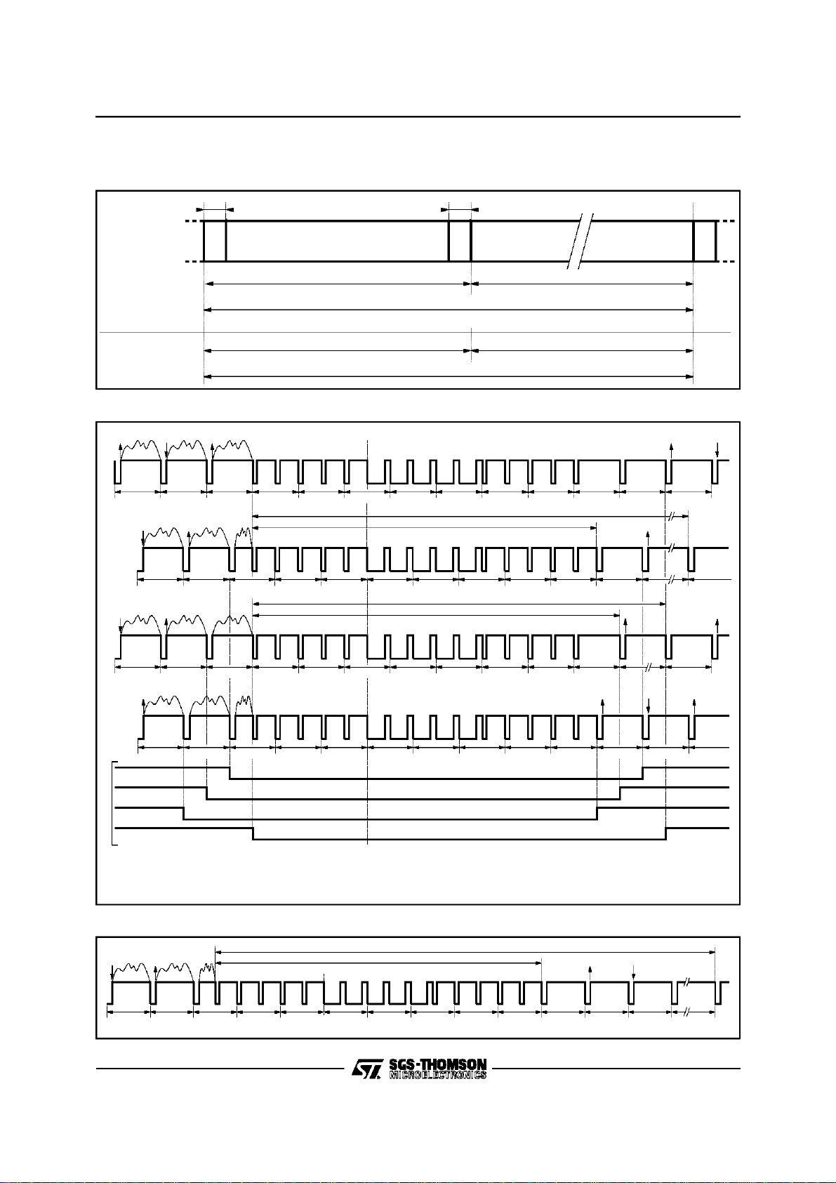
IV.4 - Master Mode
In this mode, the STV0118 supplies HSYNC and
ODDEVsyncsignals(withindependentlyprogrammable polarities) to drive other blocks. Refer to
Figure9 and 10 for timings and waveforms.
The STV0118 starts encoding and counting clock
Figure9 : ODDEVEN,VSYNC and HSYNC Waveforms
Active edge (programmable polarity)
ODDEVEN
(see Note 1)
Active edge (programmable polarity)
VSYNC
Active edge (programmable polarity)
HSYNC
(see Note 2)
Line Numbers :
SMPTE-525
CCIR-62541
Notes : 1. When ODDEVEN is a sync input, only one edge (“the active edge”) of the incoming ODDEVEN is taken into account for
synchronization. The “non-active” edge (2nd edge on this drawing) is not critical and its positionmaydiffer by H/2 from the location
shown.
2. The HSYNC pulse width indicated is valid when the STV0118 supplies HSYNC.In those slave modes where it receives HSYNC,
only the edge defined as active is relevant, and the width of the HSYNC pulse it receives is not critical.
128 T
5
2
6
3
ckref
= 4.74µs
cycles as soon as the master mode has been
loadedinto the control register (Reg.0).
Configurationbits“Syncout_ad[1:0]”(Reg4)allowto
shift the relative position of the syncsignals by up
to 3 clockcyclesto cope with any YCrCb phasing.
266
313
267
314
268
315
269
316
0118-16.EPS
Figure10 : MasterMode Sync Signals
CKREF
ODDEVEN
(out)
HSYNC
(out)
YCRCB
Note : 1. This figureis valid for bits “syncout_ad[1:0]” = default.
Active Edge
(programmable polarity)
1T
CKREF
Cr Y’
Active Edge
(programmable polarity)
Cb Y Cr Y’
Duration of HSYNC Pulse: 128 T
CKREF
0118-17.EPS
11/42
Page 12

STV0118
IV- FUNCTIONALDESCRIPTION(continued)
IV.5 - Slave Modes
Six slave modes are available : ODDEV+HSYNC
based (line-based sync), VSYNC+HSYNC based
(another type of line-based sync), ODDEV-only
based (frame-based sync), VSYNC-only based
(another type of frame-based sync), or sync-indatabased (line locked or frame locked).
ODDEV refers to an odd/even (also known as
not-top/bottom) field flag, HSYNC is a line sync
signal,VSYNCis averticalsync signal.Theirwaveforms are depicted in Figure 9. The polarities of
HSYNC and VSYNC/ODDEV are independently
programmablein all slave modes.
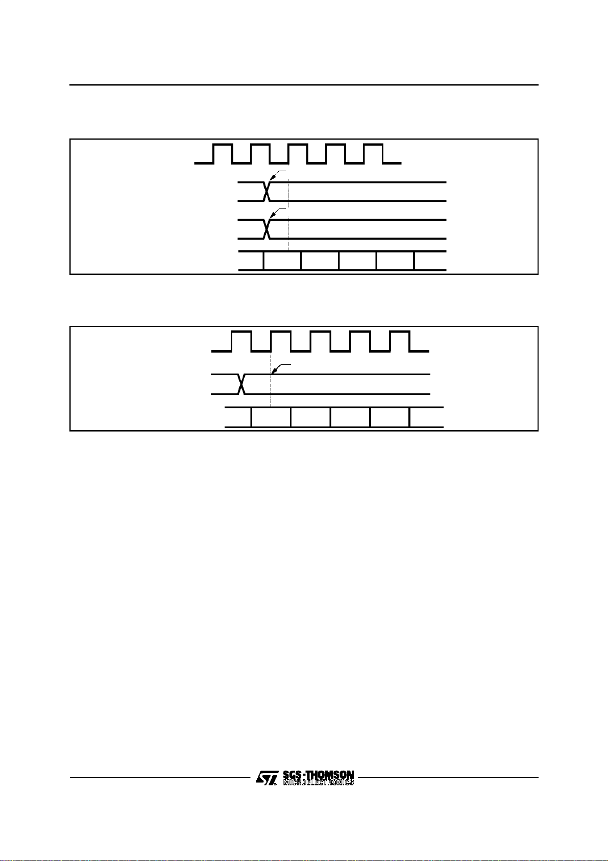
IV.5.1- Synchronizationontoa Line SyncSignal
IV.5.1.1- HSYNC+ODDEV BasedSynchronization
Synchronizationis performedon a line-by-linebasis by locking onto incoming ODDEV and HSYNC
signals. Refer to Figure 11 for waveforms and
timings. The polarities of the active edges of
HSYNCand ODDEVare programmableandindependent.
Thefirstactiveedge of ODDEVinitializesthe internal line counter but encoding of the first line does
not start until an HSYNC active edge is detected
(atthe earliest,HSYNC maytransitionat thesame
timeas ODDEV).At thatpoint, the internalsample
counter is initialized and encoding of the first line
starts. Then, encoding of each subsequent line is
individuallytriggeredby HSYNCactive edges.The
phase relationship between HSYNC and the incoming YCrCB data is normally such that the first
clockrising edgefollowingthe HSYNCactiveedge
samples “Cb” (i.e. a ‘blue’ chroma sample within
theYCrCb stream). It is however possible to internally delay the incoming sync signals
(HSYNC+ODDEV) by up to 3 clock cycles to cope
withdifferentdata/syncphasings,using configurationbits “Syncin_ad” (Reg. 4).
Figure11 : HSYNC+ ODDEVENBased SlaveMode Sync Signals
The STV0118 is thus fully slaved to the HSYNC
signal, which means that lines may contain more
or less samples than typical 525/625 system requirement.
If the digital line is shorter than its nominal value:
the samplecounteris re-initializedwhen the ‘early’
HSYNC arrives and all internal synchronization
signals are re-initialized.
If the digital line is longer than its nominal value :
the sample counter is stoppedwhen it reachesits
nominal end-of-line value and waits for the ‘late’
HSYNCbefore reinitializing.
The field counteris incrementedon each ODDEV
transition.The linecounteris reseton theHSYNC
followingeach active edge of ODDEV.
IV.5.1. 2- HSYNC + VSYNC BasedSynchron ization
Synchronizationis performed on a line-by-line basis by locking onto incoming VSYNC and HSYNC
signals. Refer to Figure 12 for waveforms and
timings. The polaritiesof HSYNC and VSYNC are
programmableand independent.
The incomingVSYNC signal is immediately transformed into a waveformidentical to the odd/even
waveform of an ODDEVsignal, therefore the behavior of the core is identical to that described
above for ODDEV+HSYNC based synchronization. Again, the p hase relationship between
HSYNC and the incoming YCrCb data is normally
such that the first clock rising edge following the
HSYNC active edge samples “Cb” (i.e. a ‘blue’
chroma sample within the YCrCb stream). It is
however possible to internally delay the incoming
sync signals (HSYNC+VSYNC) by up to 3 clock
cycles to cope with different data/sync phasings,
using configurationbits “Syncin_ad”(Reg. 4).
The field counter is incremented on each active
edge of VSYNC.
CKREF
ActiveEdge (programmablepolarity)
ODDEVEN
(in)
HSYNC
(in)
YCRCB
Note : 1. This figure is valid for bits “syncin_ad[1:0]” = default.
12/42
ActiveEdge (programmablepolarity)
Cb Y Cr Y’ Cb
0118-18.EPS
Page 13
IV- FUNCTIONALDESCRIPTION(continued)
Figure12 : HSYNC + VSYNC Based Slave Mode SyncSignals
CKREF
Active Edge (programmablepolarity)
VSYNC
(in)
Active Edge (programmablepolarity)
HSYNC
(in)
STV0118
YCRCB Cb Y Cr Y’ Cb
Notes : 1. This figure is valid for bits “syncin_ad[1:0]” = default.
2. The active edges of HSYNC and VSYNC should normally be simultaneous. Itis permissible that HSYNC transitions before
VSYNC, but VSYNC must not transition before HSYNC.
Figure13 : ODDEVENBasedSlave Mode Sync Signals
CKREF
Active Edge (programmable polarity)
ODDEVEN
(in)
YCRCB
Note : 1. Thisfigure is valid for bits “syncin_ad[1:0]” = default.
IV .5 .2-Synchro niz a tio nontoa FrameSyncSignal
IV.5.2.1 - ODDEV-only Based Synchronization
Synchronizationis performedon a frame-by-frame
basis by locking onto an incoming ODDEV signal.
A line sync signal is derived internally and is also
output as HSYNC. Refer to Figure 13 for waveformsandtimings.Thephaserelationshipbetween
ODDEVand the incomingYCrCB data is normally
such that the first clock rising edge following the
ODDEV active edge samples “Cb” (i.e. a ‘blue’
chroma sample within the YCrCb stream). It is
however possible to internally delay the incoming
ODDEVsignalby up to3 clock cyclesto copewith
different data/sync phasings, using configuration
bits“Syncin_ad” (Reg. 4).
Thefirst active edgeofODDEVtriggersgeneration
of the analog sync signals and encoding of the
incomingvideo data.Framesbeingsupposedtobe
of constantduration, the next ODDEVactive transition is expected at a precise time after the last
ODDEVdetected.
So, once an active ODDEV edge has been detected, checks that the following ODDEV are present at the expected instants are performed.
Cb Y Cr Y’ Cb
Encodingand analogsync generationcarryon unlessthreesuccessivefailsof thesechecksoccur.
In that case,threebehaviorsare possible,according to the configurationprogrammed (Reg. 1-2) :
- if ‘free-run’ is enabled, the STV0118 carries on
outputtingthe digitalline sync HSYNCand generating analog video just as though the expected
ODDEV edge had been present. However, it will
re-synchronizeontothe nextODDEVactiveedge
detected,whateverits location.
- if ‘free-run’ is disabled but bit ‘sync_ok’ is set in
configuration register1, the STV0118 sets the
active portion of the TV line to black level but
carrieson outputtingthe analogsync tips (on Ys
and CVBS) and the digital line sync signal
HSYNC.
- if ‘free-run’is disabledand the bit ‘sync_ok’is not
set, allanalog videois at blacklevel andneither
analog sync tips nor digital linesync are output.
Note that this mode is a frame-based sync mode,
asopposedtoa field-basedsyncmode,thatis,only
one type of edge (rising or falling, according to bit
‘polv’in Reg 0) is of interest to the STV0118,the
other one is ignored.
0118-19.EPS
0118-20.EPS
13/42
Page 14

STV0118
IV- FUNCTIONALDESCRIPTION(continued)
IV.5.2.2 - VSYNC only Based Synchronization
Synchronizationis performedon a frame-by-frame
basis by locking onto an incoming VSYNC signal.
An auxiliaryline sync signal HSYNC must also be
fedtotheSTV0118,whichusesittoreconstructfrom
VSYNC and HSYNC information an internal
odd/even waveform identical to that of an ODDEVENsignal.Thereforethe behaviorof the core is
identicaltothatdescribedaboveforODDEVENonly
basedsynchronization(exceptthatnothingisoutput
onHSYNCpinsinceit isan inputportin thatmode).
Notethat HSYNC is an input buthas no otheruse
than allowing the STV0118 to decide whether an
incoming VSYNC pulse flags an odd or an even
field. In other words, the STV0118 does not lock
onto HSYNC in this mode since this is NOT a
line-lockedmode.
The phase relationship between VSYNC and the
incomingYCrCb data is normallysuch thatthe first
clockrising edgefollowing the VSYNCactiveedge
samples “Cb” (i.e. a ‘blue’ chroma sample within
theYCrCb stream). It is however possible to internally delay the incoming sync signals
(VSYNC+HSYNC) by up to 3 clock cycles to cope
withdifferentdata/syncphasings,using configurationbits “Syncin_ad” (Reg. 4).
IV.5.3 - Synchronizationonto Data-embedded
SyncWords
IV.5.3.1 - ‘End-of-frame’ Word Based
Synchronization
Synchronizationis performed by extracting the 1to-0 transitions of the ‘F’ flag (end-of-frame) from
the ‘EAV’(End-of-ActiveVideo) sequenceembedded within ITU-R656 / D1 compliant digital video
streams.Both a frame sync signal and aline sync
signal are derived and are made available externally as ODDEVEN and HSYNC(see Figure14).
Thefirstsuccessfuldetectionof the‘F’flagtriggers
generationof theanalogsyncsignalsandencoding
of the incoming video data. Frames being supposed to be of constant duration, the next EAV
wordcontainingthe ‘F’flag isexpectedat a precise
Figure14 : Data (EAV)Based Slave Mode Sync Signals
time after the latestdetection.
So, once an active ‘F’ flag has been detected,
checks that the following flags are present within
the incoming video stream at the expected times
are performed.
Encodingand analogsync generationcarryon unlessthreesuccessivefailsof thesechecksoccur.
In that case, three behaviors are possible, according to the configurationprogrammed :
- if ‘free-run’ is enabled, the STV0118 carries on
- if ‘free-run’is disabledbut thebit ‘sync_ok’is setin
- if ‘free- run’isdisabledandthebit‘sync _ok ’isnotset,
The SAV and EAVwords are Hamming-decoded.
Afterdetectionof two successiveerrors,a bit is set
in the statusregister to inform the micro-controller
of thepoor transmissionquality.
IV.5.3.2- ‘End-of-line’Word Based
Synchronizationis performed by extracting the ‘F’
and ‘H’ flags from the ‘SAV’ (Start of Active Video)
and ‘EAV’ (End of Active Video) words embedded
withinITU-R656/D1compliantdigitalvideostreams.
Alinesyncsignalandaframesyncsignalarederived
internally from these flags and are output on the
HSYNC and ODDEVEN/VSYNC pins in output
mode.These signalsare also exploitedby the core
ofthecircuitwhichtreatsthem likeit treatsincoming
ODDEVENandHSYNCsignalsinHSYNC+ODDEV
basedsynchronization(seeSectionIV.5.1.1).
generatingthedigital frameandlinesyncs(ODDEVENand HSYNC)and generatinganalog video
just as though the expected ‘F’ flag had been
present. However, it will re-synchronize onto the
ne xt ‘F ’ flag dete cte d with in the inc omin g
CCIR656/D1 video stream.
the config urati on registers, the STV0118 sets the
activeportionof theTVline toblacklevel butcarries
onoutputtingtheanalogsynctips(onYsandCVBS)
andthedigitalframeandlinesyncsignalsODDEVEN
andHSYNC.
all analogvideo is at blackleveland neitheranalog
synctipsnordigitalframe/linesyncareoutput.
Synchronization
14/42
CKREF
YCRCB 00 B6 Cb Y
ODDEVEN
(out)
HSYNC
(out)
FF 00
EAV
46T
CKREF
1T
HSYNC Duration : 128T
CKREF
CKREF
0118-21.EPS
Page 15

IV- FUNCTIONALDESCRIPTION(continued)
IV.6 - Input Demultiplexer
The incoming 27Mbit/s YCrCb data is demultiplexed into a ‘blue-difference’chroma information
stream, a ‘red-difference’ chroma information
stream and a luma information stream. Incoming
databits are treatedas blue, red or lumasamples
according to their relative position with respect to
the sync signals in use and to the content of configurationbits “Syncin_ad” (slave modes) or “Syncout_ad”(mastermode).
The ITU-R601 recommendationdefines the black
luma level as Y = 16dec and the maximum white
luma level as Y = 235dec. Similarly it defines225
quantizationlevels for the color differencecomponents(Cr, Cb), centeredaround 128.
Accordingly, incoming YCrCB samples can be
saturatedin the inputmultiplexerwith thefollowing
rules :
- for Cr or Cbsamples :
Cr,Cb > 240 ⇒ Cr,Cb saturatedat 240
Cr,Cb< 16⇒Cr,Cb saturated at 16
- for Y samples :
Y > 235 ⇒ Y saturated at 235
Y<16⇒Ysaturated at 16
This avoids having to heavily saturate the composite video codes before digital-to-analog conversion in case erroneous or unrealistic YCrCb
samples are input to the encoder (there may
otherwise be overflow errors in the codes driving
the DACs), and therefore avoids genera-ting a
distorded outputwaveform.
However,in someapplications,it maybe desirable
to let ‘extreme’ YCrCb codes pass through the
demultiplexer. This is also possible, provided that
bit “maxdyn”is set in configuationregister 6.
In this case, only codes 00hex and FFhex are
overridden: if such codes are found in the active
video samples, they are forced to 01hex and FEhex.
In any case, the YCrCb codes are not overridden
for EAV/SAVdecoding
The demultiplexer is also able to handle 54Mbit/s
STV0118
YCrCbstreamsfordual encodingapplications.Refer to Section IV.17, “Dual Encoding Application 54Mbit/s YCrCB interface”.
IV.7- Sub-carrierGeneration
A Direct Digital Frequency Synthesizer (DDFS)
using a 24-bit phase accumulator, generates the
requiredcolorsub-carrierfrequency.This oscillator
feedsaquadraturemodulatorwhich modulatesthe
basebandchrominancecomponents.
The sub-carrier frequency is obtained from the
followingequation :
Fsc = (24-bit IncrementWord / 2
Hard-wired Increment Word values are available
foreachstandard(exceptfor ‘NTSC-4.43’)andcan
be automaticallyselected.Alternatively(according
to bit ‘selrst’ in Reg. 2.), thefrequencycan be fully
customized by programming other values into a
dedicated Increment Word Register (Reg. 10-11-
12). This allows for instance to encode “NTSC-
4.43” or ”PAL-M-4.43”.
This is done with thefollowingprocedure :
- Program the required increment in Registers 10
to12
- Set bit ‘selrst’ to ‘1’ in ConfigurationRegister 2
- Perform a software reset(Reg. 6).
Caution : this sets back all bits from Reg. 7
onwardsto theirdefault value, when they can be
reset.
Warning :
if a standard change occurs after the
softwarereset,theincrementvalueisautomatically
re-initialized with the hardwired or loaded value
accordingto bit selrst.
The reset phase of the color sub-carrier can also
be software-controlled(Reg. 13-14).
The sub-carrier phasecan be periodicallyresetto
its nominal value to compensatefor any drift introduced by the finite accuracy of the calculations.
Sub-carrier phase adjustment can be performed
every line, every eight field, every four field, or
every two field (Register2 bitsvalrst[1:0]).
24
) x CKREF
15/42
Page 16

STV0118
IV- FUNCTIONALDESCRIPTION(continued)
IV.8 - Burst Insertion
The color reference burst is inserted so as to
always start with a positive zero crossing of the
subcarriersine wave. The first and last half-cycles
have a reduced amplitude so that the burst envelope starts and ends smoothly.
The burst contai ns 9 or 10 sine cycles of
4.43361875MHzor3.579545MHzaccordingto the
standard programmed in the Control Register
(Reg. 0, bits std[1:0]), as follows :
- NTSC-M 9 cycles of 3.579542MHz
- PAL-BDGHI 10 cycles of 4.43361875MHz
- PAL-M 9 cyclesof 3.57561149MHz
- PAL-N 9 cyclesof 3.5820558MHz
Itis possibleto turntheburst off(no burstinsertion)
bysettingconfigurationbit ‘bursten’to0(register2).
Notes :
- Two strategies exist for burst insertion: one is tomerely
gateand shapethe subcarrierfor burstinsertion,the other
is more elaborated and is to always start the burstwith a
positive-going zero crossing. In the first case the phase
of the subcarrier when the burst starts is not controlled,
with the consequencethat some of its first and last cycles
are more heavi ly distorded. The second solution
guaranteessmooth startand endofburst witha maximum
of undistorded burst cycles and can only be beneficial to
chroma decoders, it is the solution implemented in the
STV0118.
- While the first option gave constant burst start time but
uncontrolled initial burst phase, the second solution
guarantees start on a positive-going zero crossing with
the consequence that two burst start locations arevisible
over successive lines, according to the line parity.This is
normal and explained below.
- In NTSC, the relation between subcarrier frequency and
line length creates a 180o subcarrier phase difference
(with respect to the horizontal sync) from one line to the
next according to the line parity. So if the burst always
startswith thesame phase (positive-goingzerocrossing),
this means the burst will be inserted at time Xor at time
/2 after the horizontal sync tip according to the
X+T
NTSC
line parity, where T
NTSC burst.
- With PAL, a similar rationale holds, and again there will
be two possible burst start locations. The subcarrier
phasedifference (withrespect tothehorizontalsync) from
one line to the next in that case is either 0 or 180o with
the following series: A-A-B-B-A-A-...-etc. where A
denotes ‘A-type’ bursts and B denotes ‘B-type’ bursts,
A-type and B-type being 180° out of phase with respect
to the horizontal sync. So 2 locations are possible, one
for A-type,the other forB-type (see Figure 8).
- This assumes a periodic reset of the subcarrier is
automatically performed (see bits valrst[1:0] in Reg 2).
Otherwise, over severalframes, the start of burst will drift
within an interval of one a subcarrier’s cycle. THIS IS
NORMAL and means the burst is correctly locked to the
colors encoded. Theequivalent effect witha gatedburst
approachwould be the following : thestart locationwould
be fixed but the phase with which the burst starts (with
respect to the horizontal sync) would be drifting.
IV.9 - LuminanceEncoding
The demultiplexed Y samples are band-limited
and interpolated at CKREFclock rate. The resulting luminance signal is properly scaled before
insertion of any Closed-captions, CGMS or
Teletext data and synchronization pulses.
is the duration of one cycle of the
NTSC
Theinterpolationfiltercompensatesforthesin(x)/x
attenuationinherent to D/A conversionand greatly
simplifies the outputstagefilter(referto Figures15
to17 for characteristiccurves).
Figure 15 : Luma Filtering Including DAC
Attenuation
0
-5
-10
-15
-20
-25
-30
Amplitude (dB)
-35
-40
01234567 9108111213
6
Frequency (x10
) (Hz)
Figure 16 : Luma Filtering with 3.58MHz Trap,
IncludingDAC Attenuation
0
-5
-10
-15
-20
-25
-30
Amplitude (dB)
-35
-40
01234567 9108 111213
6
Frequency (x10
) (Hz)
Figure 17 : Luma Filtering with 4.43MHz Trap,
IncludingDAC Attenuation
0
-5
-10
-15
-20
-25
-30
Amplitude (dB)
-35
-40
01234567 9108 111213
6
Frequency (x10
) (Hz)
0118-22.EPS
0118-23.EPS
0118-24.EPS
16/42
Page 17

IV- FUNCTIONALDESCRIPTION(continued)
In addition, the luminance that is added to the
chrominanceto createthe compositeCVBS signal
can be trap-filtered at 3.58MHz (NTSC) or
4.43MHz (PAL). This allows to cope with application oriented towards low-end TV sets which are
subject to cross-color if the digital source has a
wide luminance bandwidth (e.g. some DVD
sources).Notethat thetrapfilterdoes notaffect the
S-VHSluminance output nor the RGB outputs.
A7.5 IRE pedestal can be programmedif needed
withall standards(seeReg1,bitsetup).Thisallows
in particular to encode Argentinian and non-Argentinian PAL-N, or Japanese NTSC (NTSC with
no set-up).
A programmable delay can be inserted on the
luminance path to compensate any chroma/luma
delay introduced by off-chip filtering (chroma and
lumatransitionsbeingcoincidentattheDACoutput
withdefault delay) (Reg3, bits del[2:0]).
IV.10 - ChrominanceEncoding
U and V chroma components are computed from
demultiplexedCb, Cr samples. Beforemodulating
thesubcarrier,theseare band-limitedand interpolated at CKREF clock rate.This processingeases
the filtering following D/Aconversion and allows a
more accurate encoding.A set of 4 differentfilters
is availablefor chroma filtering to fit a wide variety
of applications in the different standards and includefiltersrecommendedbyITU-RRec624-4and
SMPTE170-M.The available 3dB bandwidthsare
1.1, 1.3, 1.6 or 1.9MHz, refer to Figures 18 to 22
for the various frequency responses (Reg1, bits
flt[1:0]).
Thenarrowerbandwidthsareusefulagainstcrossluminanceartefacts,the widerbandwidthsallowto
keep higher chroma contents and then an improvedimage quality.
IV.11 - Composite Video Signal Generation
The composite video signal is created by adding
the luminance (after optional trap filtering, Reg 3
bits entrap and trap_pal) and the chrominance
components.Asaturationfunctionisincludedinthe
adder to avoid overflow errors should extreme
luminance levels be modulated with highly saturated colors (this does not correspond to natural
colors but may be generated by computers or
graphicengines).
A‘colorkilling’function isavailable(Reg 1, bitcoki)
wherebythe compositesignal contains no chrominance, i.e. replicates the trap-filtered luminance.
STV0118
Note that this function does not suppress the
chrominanceon the S-VHS outputs (nevertheless
suppressing the S-VHS chrominance is possible
using bit “bkg_c”in Reg 5).
Figure 18 : Various Chroma Filters Available
+ RGB Filter
1
0
-1
-2
-3
-4
-5
-6
Amplitude(dB)
-7
-8
-9
0 0.5 1.5 21 2.5 3 3.5
f
=1.1
3
Frequency(x106) (Hz)
f
=1.3
3
Figure 19 : 1.1MHzChroma Filter (flt = 00)
0
-5
-10
-15
-20
-25
Amplitude (dB)
-30
-35
-40
0 2 4 6 8 10 12 14
Frequency (x10
Figure 20 : 1.3MHzChroma Filter (flt = 01)
0
-5
-10
-15
-20
-25
Amplitude (dB)
-30
-35
-40
0 2 4 6 8 10 12 14
Frequency(x10
f3=1.6
6
) (Hz)
6
) (Hz)
RGB
f3=1.9
f
=2.45
3
0118-25.EPS
0118-26.EPS
0118-27EPS
17/42
Page 18

STV0118
IV- FUNCTIONALDESCRIPTION(continued)
Figure21 : 1.6MHzChroma Filter (flt = 10)
0
-5
-10
-15
-20
-25
Amplitude (dB)
-30
-35
-40
0 2 4 6 8 10 12 14
Frequency(x10
Figure22 : 1.9MHzChroma Filter (flt = 11)
0
-5
-10
-15
-20
-25
Amplitude (dB)
-30
-35
-40
0 2 4 6 8 101214
Frequency(x10
IV.12 - RGBEncoding
After demultiplexing, the Cr and Cb samples feed
a 4 times interpolation filter. The resulting baseband chroma signal has a 2.45MHz bandwidth
(Figure 23) and is combinedwith the filtered luma
componenttogenerateR,G,Bsamplesat27MHz.
Figure23 : RGBChroma Filtering
0
-5
-10
-15
-20
-25
Amplitude (dB)
-30
-35
-40
0 2 4 6 8 101214
Frequency(x10
6
) (Hz)
6
) (Hz)
6
) (Hz)
IV.13- ClosedCaptioning
Closed-captions(or data from an Extended Data
Serviceas defined by the Closed-Captions specification)can be encodedby thecircuit. The closed
caption data is delivered to the circuit through the
2
I
C interface. Two dedicated pairs of bytes (two
bytes per field), each pair preceded by a clock
run-in anda start bit canbe encodedand inserted
on the luminance path on a selected TV line. The
ClockRun-In and Start code are generatedby the
STV0118.
Closed-captiondata registersare double-buffered
so that loading can be performed anytime, even
duringline 21/284 or any otherselected line.
0118-28.EPS
Userregister39 (resp. 41) containsthe firstbyte to
send(LSBfirst)afterthestartbitonthe appropriate
TVline in field1 (resp.field2),anduserregister40
(resp. 42) contains the second byte to send. The
TV line number where data is to be encoded is
programmble (Reg. 37, 38). Lines that may be
selectedinclude those usedby the StarSightdata
broadcastsystem.Closed-captionsdatahaspriority over CGMSprogrammed for the sameline.
Theinternal Clock Run-Ingenerator is based on a
DirectDigital FrequencySynthesizer. The nominal
instantaneousdatarateis503.5kbit/s(i.e. 32times
theNTSC line rate). DataLOWcorrespondsnominallyto 0IRE, data HIGHcorrespondsto 50 IREat
the DAC outputs. Refer to Figure 24.
0118-29.EPS
When closed-captioning is on (bits cc1/cc2 in
Reg.1),the CPU shouldloadthe relevantregisters
(reg.39 and 40, or 41 and42) once everyframeat
most(althoughthere is in fact some margin due to
thedouble-buffering).Twobitsare setin thestatus
registerin case of attemptsto loadthe closed-caption data registers too frequently, these can be
used to regulateloading rate.
Figure 24 : ExampleClosed-captionWaveform
300
250
200
150
LSB
100
50
0118-30.EPS
0
10µs
27.35µs
13.9µs
7 cycles
of 504kHz
Transition
Time : 220ns
61µs
t
0118-31.EPS
18/42
Page 19

IV- FUNCTIONALDESCRIPTION(continued)
The closed caption encoderconsiders that closed
caption data has been loaded and is valid on
completion of the write operation into register 40
forfield1,intoregister42forfield2.Ifclosedcaption
encodinghasbeenenabledandnonew databytes
have been written into the closed caption data
registerswhentheclosedcaptionwindow startson
theappropriateTV line,then thecircuitoutputstwo
US-ASCIINULLcharacterswithoddparityafterthe
start bit.
IV.14 - CGMSEncoding
CGMS (Copy Generation Management System also known as VBID and described by standard
CPX-1204 of EIAJ) data can be encoded by the
circuit. Three bytes (20 significant bits) are deliveredtothechipviatheI2Cinterface.Tworeference
bits (‘1’ then ‘0’) are encodedfirst, followedby 20
bitsof CGMSdata (includinga CyclicRedundancy
Checksequence,not computedby the deviceand
supplied to it as part of the 20 data bits). The
reference bits are generated locally by the
STV0118.Refer to Figure 25 for a typical CGMS
waveform.
WhenCGMS encodingisenabled,the CGMS(see
bit encgms in Reg 3) waveform is continously
present once in each field, on lines 20 and 283
(SMPTE-525line numbering).
TheCGMS data registeris double-buffered,which
means that it can be loaded anytime (even during
line 20/283) without any risk of corrupting CGMS
data that could be in the process of being encoded.The CGMS encoder considers that new
CGMSdata has been loaded and is valid on completionof the writeoperation into register33
Figure25 : ExampleCGMSWaveform
300
250
200
150
LSB
100
50
0
11µs
Word 0
6 bits
Bit 1 Bit 20
t
48.7µs
Word 1
4 bits
Word 2
4 bits
CRCC
6 bits
STV0118
IV.15- TeletextEncoding
TheSTV0118is ableto encodeTeletextaccording
to the “CCIR/ITU-R Broadcast Teletext System B”
specif ication, also known as “World System
Teletext”.
In DVB applications, Teletext data is embedded
withinDVBstreamsasMPEGdatapackets.Itisthe
responsibility of a “TransportLayer Processing” IC
(or demultiplexer), like SGS-Thomson’s ST20based“TP2”,to sortout incomingdatapacketsand
inparticulartostoreTeletextpacketinabuffer,which
thenpassesthem to the STV0118on request.
IV.15.1- Signals Exchanged
The STV0118and the Teletext buffer exchange 2
signals: TTXS (Teletext Synchronization) going
fromthe STV0118to theTeletextBuffer and TTXD
(TeletextData) goingfrom the TeletextBuffertothe
STV0118.
The TTXS signal is a request signal generated on
selected lines. In response to this signal, the
Teletextbufferisexpectedto send360Teletextbits
to the STV0118for insertion of a Teletextline into
the analog video signal.
Thedurationof theTTXSwindowis 1402reference
clockperiods(51.926µs),whichcorrespondsto the
duration of 360 Teletext bits (see Transmission
Protocolbelow).
Following the TTXS rising edge the encoder expectsdata fromtheTeletextbufferaftera programmable number (2 to 9) of 27MHz master clock
periods.Dataistransmittedsynchronouslywiththe
master clock at an average rate of 6.9375Mbit/s
accordingto the protocol described below. It consists, in orderof transmission, of 16 Clock Run-In
bits, 8 Framing Code bits and the 336 bits (42
bytes)that represent one Teletext packet.
IV.15.2- TransmissionProtocol
In order to transmit the Teletext data bits at an
average rate of 6.9375Mbit/s, which is about
1/3.89 times the master clock frequency,the followingscheme is adopted:
The 360-bit packet is regarded as nine 37-bit sequences plus one 27-bit sequence. In every sequence, each Teletextdata bit is transmitted as a
successionof4identicalsamplesat27 Msample/s,
exceptfor the 10th, 19th, 28th and 37th bitsof the
sequence which are transmitted as a succession
of 3 identical samples.This protocol is compatible
withSGS-Thomson’sST-20 based TranportLayer
IC (“TP2”).
0118-32.EPS
19/42
Page 20

STV0118
IV- FUNCTIONALDESCRIPTION(continued)
Figure26 : “TTXSRising” to “First Valid Sample”Delay for txdl[2:0] = 0
CKREF
TTXS
TTXD
(txdl[2:0] + 2) T
NotValid Bit 1 Bit 2
CKREF
IV.15.3 - Programming
IV.15.3.1- ’TTXSRising’ to ’First Valid
Sample’Delay Programming
TheencoderexpectstheTeletextbuffertoclockout
the first Teletextdata sampleon the (2+N)thrising
edge of the master clock followingthe risingedge
of TTXS (Figure 26 depicts this graphically for
N=0). ’N’ is programmablefrom 0 to 7 (i.e. overall
delayis programmablefromTWO to NINE 27MHz
cycles)via 3 dedicatedbits locatedin the ConfigurationRegister4 : “txdl[2:0]”.
IV.15.3.2- TeletextLine Selection
Five dedicatedregisters allowto programTeletext
encodingin various areas of the Vertical Blanking
Interval(VBI) of eachfield. Atotal of 4 such areas
(i.e. blocks of contiguous Teletext lines) can independently be defined within the two VBIs of one
frame(e.g.2blocksineachVBI,or3 blocksinfield1
VBI and one in field2 VBI, etc.). Further, under
certaincircumstances,it ispossible to define up to
4 areas in each VBI.
Programming isperformed using4 “Teletext Block
Definition” registers (TTXBD1, TTXBD2,
TTXBD3,TTXBD4)and a “TeletextBlockMapping”
register(TTXBM). Refer to the descriptionof user
registers34 to 38 fordetails.
IV.15.4 - TeletextPulse Shape
Theshapeandamplitudeofa singleTeletextpulse
aredepictedin Figure27,itsrelativepowerspectral
density is given in Figures 28 and 29 and is substantiallyzero at frequencies above 5MHz, as re-
quiredby the WorldSystemTeletextspecification.
Figure 27 : Shape and Amplitudeof a Single
TeletextSymbol
70
60
50
40
IRE
30
20
10
0
-150 -100 -50 0 50 100 150
(ns)
+144ns-144ns
Figure 28 : Linear PSD Scale
1
0.9
0.8
0.7
0.6
0.5
0.4
PSD (dB)
0.3
0.2
0.1
0012345678
(x106) (Hz)
0118-33.EPS
0118-34.EPS
0118-35.EPS
20/42
Page 21

IV- FUNCTIONALDESCRIPTION(continued)
Figure29 : LogarithmicPSD Scale
0
-10
-20
-30
-40
-50
PSD (dB)
-60
-70
-80
012345678
(x106) (Hz)
2
IV.16 - I
An external micro-controller controlsthe STV0118
viaanI
registers. The I
2
C protocol”(upto 400kHz- andpotentiallymore).
I
Thedefault I
C Bus
2
Cbusby writingintoorreadingfrominternal
2
C interface supports the “fast
2
C addresses of theSTV0118 are :
- in write mode : “01000000”(40 hex)
- in read mode : “01000001”(41 hex)
After a hardware reset, it is these addresses that
the STV0118recognizes.
It is possibleto modify the default I
tiing the TTXS/CSI2C pin to logic ‘1’ and validating the change by writing into a dedicated bit in
Register 6.
Inthat case,the STV0118hasa new I
- in writemode : “01000010”(42 hex)
- in readmode : “01000011”(43hex)
OncetheI
2
C addresshas beenchanged,it cannot
bemodifed anymoreuntil thenext hardwarereset.
Note that these I
those used by the STV0117/STV0117A/STV0119
0118-36.EPS
(others SGS-THOMSON PAL/NTSC Digital En-
2
coder).
It is expected that I
mally be needed for dual encoding applications.
Theexact procedure to changethe I
isdetailedbelow,in thesectionthat dealswith dual
encodingapplications.
Write and read operations are described in Figures30 and 31.
Figure30 : I2C Write Operation (default addressat power-on, CSI2C≠’1’)
STV0118
2
C address by
2
C address:
C addresses are the same as
2
C address changes will nor-
2
C addresses
SCL
ACK by
STV0119
R/W
SDA
I2C Slave Address 40h ACKby
SCL
D7 D6 D5 D4 D3 D2 D1 D0 D7 D6 D5 D4 D3 D2 D1 D0 D7 D6 D5 D4 D3 D2 D1 D0
SDA
Data Byte2 Data Byte 3 Data Byte n Stop
A7 A6 A5 A4 A3 A2 A1 A0 D5 D4 D3 D2 D1 D0
STV0119
LSB AddressStart
ACK by
STV0119
ACK by
STV0119
D6D7
Figure31 : I2C ReadOperation(default address at power-on,CSI2C≠’1’)
SCL
SDA
SCL
SDA
Start
R/W
I2C SlaveAddress 40h
R/W
I2C SlaveAddress 41h
A7 A6 A5 A4 A3 A2 A1 A0
STV0119
D7 D6 D5 D4 D3 D2 D1 D0
ACKby
STV0119
LSB Address
Data Byte 1
ACKby
STV0119
ACK by
micro
StopACK by
D7 D6 D5 D4 D3 D2 D1 D0
Data Byte nStart
DataByte 1
ACKby
STV0119
ACK by
micro
ACK by
STV0119
Stop
0118-37.EPS
0118-38.EPS
21/42
Page 22

STV0118
IV- FUNCTIONALDESCRIPTION(continued)
IV.17- Dual Encoding Application with 54Mbit/s YCrCb Interface
The STV0118 is able to interface with SGSTHOMSON’s MPEG decoders capable of supplying a 5 4-Mbit/ s YCrCB multiplex, like the
STi3520M. This multiplex embeds two 27Mbit/s
YCrCbvideo streams,one with OSD contents and
the other without OSD content (see Figure 32).
Note that the frequency of the reference clock
supplied to the encoder is still 27MHz, only both
edgesare usedin the interface.
The MPEG decoder being usually slaved to the
encoder,if two encodersare to beusedin parallel,
oneof themmust be masterand the other must be
slave. Figure 33 shows a typical dual encoding
application(althoughotherapplicationswhere two
STV0118’sare slaveare possible).
It is also necessary to be able to control independently the encoders. One solution is to have
two separate I
runningfromthe microcontroller(thisis possibleon
SGS-THOMSON’s ST20, which features two I
busses),another solutionis to change the I
2
C busses (one for each encoder)
2
C chip
2
C
addressof one of the STV0118.
This can be donewith the followingprocedure :
- If no Teletext is required, tie pin TTXS/ CSI2Cof
Figure32 : 54Mbit/sDual YCRCB Stream
the 1st encoderto ‘0’.
- If Teletext encoding is needed, connect the
TTXS/CSI2Cpin of the first encoder to boththe
TTXS input pin of the Teletext Buffer / Transport
IC (e.g. SGS-Thomson’sTP2) and a pull-down
resistor (needed for power-on configuration).
- Connect TTXS/CSI2C of the second encoder to
logic ‘1’.
- Before performingany Teletext-relatedprogramming, set to ‘1’ bit “chgi2c” in configurationregister6.
Onhardware reset, both encoders have the same
defaultI
2
C address(40-41hex).When bit “chgi2c”
toggles to ‘1’, the I
(withTTXS/CSI2Cpulledlow) keepsunchangedat
40-41hex, whilst the I
encoder (with TTXS/CSI2C = ‘1’) switches to 4243hexand can no more be changeduntil the next
hardwarereset.
2
After I
C address change, the second encoder
mustbeprogrammedtochoosetheYCRCbincomingdata streamon thefalling edge ofCKREF (see
bit ’nosd’in configurationregister 3).
2
C addressof the first encoder
2
C address of the second
CKREF
(27MHz)
54Mbit/s
YCRCB Stream
Cb
nosd
Cb
osd
Y
nosd
Y
osd
Cr
nosd
Cr
osd
Y’
nosd
Y’
osd
Cb
nosd
Cb
nosd
0118-39.EPS
22/42
Page 23

IV- FUNCTIONALDESCRIPTION(continued)
Figure33 : TypicalDual EncodingApplication
STV0118
27MHz
3.3V
V
ODDEVEN
HSYNC
YCrCb[7:0]
MPEG Decoder
(e.g. STi3520M)
V
SS
27MHz
ODDEVEN
HSYNC
DD
Frame Sync
8
Interface
Line Sync
8
27MHz
3.3V
54MHz
Digital Video
Data
Transport IC
(ST20TP2)
V
DD
TTXS
(Demultiplexer +
CPU+ Teletext
Buffer)
V
SDA
SCL
SS
STV0118
(Master)
54MHz
Bit nosd = 0
TTXS/CSI2C
R
pull-down
B/CVBS
CVBS
V
SS
=47kΩ
G/Y
R/C
SCL
SDA
DD
3.3V
pull-up
R
3.3V
3.3VV
With OSD
With OSD
pull-up
R
For TV Set
3.3V
STV0118
(Slave)
SCL
SDA
G/Y
R/C
B/CVBS
CVBS
WithoutOSD
WithoutOSD
ForVCR
0118-40.EPS
8
27MHz
TTXS/CSI2C
(See Bit chgi2c)
V
SS
ODDEVEN
HSYNC
54MHz
Interface
Bit nosd = 1
23/42
Page 24

STV0118
IV- FUNCTIONALDESCRIPTION(continued)
IV.18 - LineSkip / LineInsert Capability
This patented feature of the STV0118 offers the
possibility to cut the cost of the application by
suppressingthe need for a VCXO.
Ideally, the master clock used on the application
board and fed to the MPEG decoding IC would
haveexactly samefrequencyas theclock thatwas
used when the MPEG data was encoded. Obviously this is not realistic; up to now a solution
commonlychosenistodynamicallyadjusttheclock
onthe boardas closeto the‘ideal’clockas possible
with the help of time stamps embeddedwithin the
MPEG stream. Such a kind of tracking often involvesthe use of a VCXO : when the MPEG data
bufferfillsuptomorethansomethresholdthe clock
frequency is increased, when it empties down to
some other threshold the clock frequency is lowered.
The STV0118 offers an alternative, cost-saving
solution: by programming the two bits jump and
dec_ninc in configuration Reg6, the STV0118 is
able to reduce or increase the length of some
framesin a waythat will not introducevisible artefacts (even if comb-filtering is used). These bits
should be set according to the level of the MPEG
data buffer. Refer to Section VI.2 Register 6,
Register 9 and Registers 21-22-23 for complete
bit description.
Operationwith the STV0118as sync master is as
follows:
- If the MPEG data buffersfills uptoo much:set bit
“jump”to‘1’and bit“dec_ninc”to ‘1’.TheSTV0118
will reduce the length of the current frame (Bit
“jump”will thenautomaticallybe resetto ‘0’).
- IftheMPEGdatabuffersemptiestoomuch:set bit
“jump”to ‘1’andbit “dec_ninc”to‘0’.TheSTV0118
will increase the length of the current frame (Bit
“jump”will then automaticallyberesetto ‘0’).
These operationscan be repeateduntil the MPEG
data buffer is insideits fixed limits.
It is also possible to use the line skip/repeatcapabilityin non-interlacedmode.
This functionalityof the STV0118is alsoavailable
in slave mode, in this case the sync signals supplied to the STV0118must be in accordance with
the modifiedframe lengthes programmed.
IV.19- CVBS, S-VHS and RGB Analog Outputs
Four out of six video signals (composite CVBS,
S-VHS(Y/C)and RGB)canbedirectedto 4 analog
output pins through 9-bit D/Aconverters operating
at thereferenceclock frequency.
The available combinations (see bit ‘rgb_nyc’ in
Reg5) are :
S-VHS(Y/C) + CVBS + CVBS1
or : R, G, B + CVBS1.
Asingle external analog power supply pair is used
for all DACs, but two independentpairs of current
and voltage references are needed. Each current
referencepin is normallyconnectedexternallyto a
resistor tied to the analogue ground, whilst each
voltage reference pin is normally connected to a
capacitancetied to the analogueground.
The internalcurrent sourcesare independentfrom
the positive supply, thanks to a bangap, and the
consumptionof theDACs isconstantwhateverthe
codes converted.
Any unused DAC may be independentlydisabled
by software, in which caseits outputis at ‘neutral’
level(blanking for luma andcompositeoutputs,no
color for chroma output, black for RGB outputs).
For applications where a single CVBS output is
required, the RGB/CVBS+S-VHS Triple DAC
should be disabled and Pins I
REF(RGB)
, VR_RGB
tied to analog power supply.
24/42
Page 25

STV0118
V - CHARACTERISTICS
V.1 - Absolute MaximumRatings
Symbol Parameter Value Unit
V
V
V
I
REF
T
T
P
V.2 - ThermalData
Symbol Parameter Value Unit
R
th(j-a)
V.3 - DC Electrical Characteristics
T
amb
Symbol Parameter Test Conditions Min. Typ. Max. Unit
SUPPLY
V
V
I
DDA
I
DIGITAL INPUTS
V
V
C
SDA OUTPUT
V
DIGITAL OUTPUT
V
V
D/A CONVERTER
RI
V
ILE LF Integral Non-linearity RI
DLE LF Differential Non-linearity RI
Notes : 1. This product withstands 1.4kV (The MIL883C Norm requires 2.0kV).
DC Supply Voltage -0.3, 4.0 V
DDx
Digital Input Voltage -0.3, VDD+ 0.3 V
IN
Digital Output Voltage -0.3, VDD+ 0.3 V
OUT
Analog Input Reference Current 2 mA
Operating Temperature 0, +70
oper
Storage Temperature -40, +150
stg
Total Power Dissipation 500 mW
tot
DC Junction-Ambient Thermal Resistance
Typ. 76 °C/W
with sample soldered on a PCB
=25°C/70°C, V
Analog Positive Supply Voltage 3.0 3.3 3.6 V
DDA
Digital Supply Voltage 3.0 3.3 3.6 V
DD
DDA=VDD
Analog Current Consumption RI
Digital Current Consumption 20 35 50 mA
DD
Input Voltage Low level (any other pins) 0.8 V
IL
Input Voltage
IH
SCL and SDA
Except SCL and SDA
Input Leakage Current
I
L
Input Pins (see note 2)
Bi-directional Pins
Input Capacitance
IN
Input Pins
Bi-directional Pins
Output Voltage Low level, IO= 2mA 0.4 V
L
Output Voltage High level (IOH= -4mA) 2 V
OH
Output Voltage Low level (IOL= 4mA) 0.6 V
OL
Resistance for reference Current
REF
Source for 3 D/A Converters
Output Voltage Dyn RI
O
DAC to DAC VOmaxcode(tri-DAConly) RI
This product withstands 150V (The EIAJ Norm requires 200V).
2. The highvalue for input Pins is due to internal pull-down resistance.
=3.3V,unless otherwisespecified
=1.2kΩ,RL= 200Ω,
REF
= 50pF, CKREF = 27MHz,
C
L
= 3.6V autotest mode,
V
DD
static input signals
High level (any other pins)
min or VIHmax
V
IL
I
REF=VREF
REF
(Max. code - Min. Code)
REF
REF
REF
/RI
REF,VREF
= 1.2kΩ,RL= 200Ω
= 1.2kΩ,RL= 200Ω 3%
= 1.2kΩ,RL= 200
= 1.2kΩ,RL= 200
20 50 mA
2.0
2.0
-10
-10
0.1
5
= 1.12V typ. 1.2 k
0.95 1.10 V
Ω ±
Ω ±
0.5 LSB
4.5
V
DD
8010µA
1 LSB
o
o
µA
pF
pF
C
C
V
Ω
PP
25/42
Page 26

STV0118
V - CHARACTERISTICS (continued)
V.4 - ACElectrical Characteristics
=25°C/70°C, V
T
amb
DDA=VDD
Symbol Parameter Test Conditions Min. Typ. Max. Unit
DIGITAL INPUT (YCRCB[7:0], HSYNC, VSYNC/ODDEVEN)
tsu Input Data Set-up Time CKREF rising edge, CKREF = 27MHz 6 ns
tho Input Data Hold Time CKREF rising edge, CKREF = 27MHz 3 ns
ACTIVE PERIOD FOR NRESET
tRSTL Input Low Time 200 ns
REFERENCE CLOCK : CKREF
1/tC_REF Clock Frequency 27 MHz
tD_REF Clock Duty Cycle 35* 65* %
tR_REF Clock Rise Time 5 ns
tF_REF Clock Fall Time 5ns
2
C CLOCK : SCL
I
tC_SCL Clock Cycle Time Rpull_up = 4.7kΩ 2MHz
tD_SCL Clock Duty Cycle 50 %
tL_SCL LOW Level Cycle Rpull_up = 4.7k
DIGITAL OUTPUTS
td_HSYNC Delay Time CKREF rising edge
td_ODDEVEN Delay Time CKREF rising edge
* In case of double encoding these values must be compatible with the ycrcb transmitter.
=3.3V,unless otherwisespecified
Ω
CKREF = 27MHz, C
CKREF = 27MHz, C
= 50pF
L
= 50pF
L
250 ns
10 ns
10 ns
26/42
Page 27

STV0118
VI- REGISTERS
VI.1- RegisterMapping
configuration0 R/W 00 std1 std0 sync2 sync1 sync0 polh polv freerun
configuration1 R/W 01 blkli flt1 flt0 sync_ok coki setup cc2 cc1
configuration2 R/W 02 nintrl enrst bursten xxx selrst rstosc valrst1 valrst0
configuration3 R/W 03 entrap trap_pal encgms nosd del2 del1 del0 xxx
configuration4 R/W 04 syncin
_ad1
configuration5 R/W 05 rgb_nyc bkcvbs1 reserved reserved bk_ys bk_c bk_cvbs dacinv
configuration6 R/W 06 softreset jump dec_ninc free_jump xxx xxx chgi2c maxdyn
reserved xxx 07 xxx xxx xxx xxx xxx xxx xxx xxx
reserved xxx 08 xxx xxx xxx xxx xxx xxx xxx xxx
status R 09 hok atfr b2_free b1_free fieldct2 fieldct1 fieldct0 jumping
increment_dfs R/W 10 d23 d22 d21 d20 d19 d18 d17 d16
increment_dfs R/W 11 d15 d14 d13 d12 d11 d10 d9 d8
increment_dfs R/W 12 d7 d6 d5 d4 d3 d2 d1 d0
phase_dfs R/W 13 - - - - - - o23 o22
phase_dfs R/W 14 o21 o20 o19 o18 o17 o16 o15 o14
reserved xxx 15 xxx xxx xxx xxx xxx xxx xxx xxx
reserved xxx 16 xxx xxx xxx xxx xxx xxx S xxx
chipid R 17 0 1 1 1 0 1 1 1
revid R 18 0 0 0 0 0 0 0 1
reserved R/W 19 xxx xxx xxx xxx xxx xxx xxx xxx
reserved R/W 20 xxx xxx xxx xxx xxx xxx xxx xxx
line_reg R/W 21 ltarg8 ltarg7 ltarg6 ltarg5 ltarg4 ltarg3 ltarg2 ltarg1
line_reg R/W 22 ltarg0 lref8 lref7 lref6 lref5 lref4 lref3 lref2
line_reg R/W 23 lref1 lref0 - - - - - cgms_bit_1-4 R/W 31 - - - - bit1 bit2 bit3 bit4
cgms_bit_5-12 R/W 32 bit5 bit6 bit7 bit8 bit9 bit10 bit11 bit12
cgms_bit_13-20 R/W 33 bit13 bit14 bit15 bit16 bit17 bit18 bit19 bit20
ttx_block_1_def. R/W 34 ttxbs1.3 ttxbs1.2 ttxbs1.1 ttxbs1.0 ttxbe1.3 ttxbe1.2 ttxbe1.1 ttxbe1.0
ttx_block_2_def. R/W 35 ttxbs2.3 ttxbs2.2 ttxbs2.1 ttxbs2.0 ttxbe2.3 ttxbe2.2 ttxbe2.1 ttxbe2.0
ttx_block_3_def. R/W 36 ttxbs3.3 ttxbs3.2 ttxbs3.1 ttxbs3.0 ttxbe3.3 ttxbe3.2 ttxbe3.1 ttxbe3.0
ttx_block_4_def. R/W 37 ttxbs4.3 ttxbs4.2 ttxbs4.1 ttxbs4.0 ttxbe4.3 ttxbe4.2 ttxbe4.1 ttxbe4.0
ttx_block_map R/W 38 ttxbmf1.1 ttxbmf1.2 ttxbmf1.3 ttxbmf1.4 ttxbmf2.1 ttxbmf2.2 ttxbmf2.3 ttxbmf2.4
c.c.c.F1 R/W 39 opc11 c117 c116 c115 c114 c113 c112 c111
c.c.c.F1 R/W 40 opc12 c127 c126 c125 c124 c123 c122 c121
c.c.c.F2 R/W 41 opc21 c217 c216 c215 c214 c213 c212 c211
c.c.c.F2 R/W 42 opc22 c227 c226 c225 c224 c223 c222 c221
cclif1 R/W 43 xxx xxx xxx l1_4 l1_3 l1_2 l1_1 l1_0
cclif2 R/W 44 xxx xxx xxx l2_4 l2_3 l2_2 l2_1 l2_0
reserved xxx 45 xxx xxx xxx xxx xxx xxx xxx xxx
... ... ... ... ... ... ... ... ... ... ...
reserved xxx 63 xxx xxx xxx xxx xxx xxx xxx xxx
syncin
_ad0
syncout
_ad1
syncout
_ad0
aline txdl2 txdl1 txdl0
27/42
Page 28

STV0118
VI- REGISTERS(continued)
VI.2- RegisterContents and Description
(*)= DEFAULTmode when NRESET pin is active(LOW level)
REGISTER_0 - Configuration0
MSB LSB
Content std1 std0 sync2 sync1 sync0 polh polv freerun
Default 10010010
std[1:0] std1 std0 Standard Selected
0
0
PALBDGHI
0
1
PALN (see bit set-up)
(*)
sync[2:0]sync2 sync1 sync0 Configuration
(*)
1
0
NTSC M
1
1
Note 1 : Standard on hardware reset is NTSC; any standardmodification selects automatically the right parameters for
PAL M
correct subcarrier generation.
(referto FunctionalDescription, SectionsIV.4 and IV.5)
0
0
0
0
1
1
1
1
Caution : In VSYNC-only based slave mode (sync[2:0]=”100”), HSYNC is nevertheless needed as an input.
0
0
1
1
0
0
1
1
Refer to Functional Description, Section IV.5.2.2.
0
1
0
1
0
1
0
1
ODDEVENbased SLAVEmode (frame locked)
F onlybased SLAVEmode (framelocked)
ODDEV+HSYNC basedSLAVEmode (line locked)
‘F’+’H’based SLAVEmode (line locked)
VSYNC-onlybased SLAVEmode (framelocked) (see Note)
VSYNC+HSYNC based SLAVEmode (line locked)
MASTER mode
AUTOTESTmode (color bar pattern)
polh Synchro : active edge of HSYNC selection(when input)
or polarityof HSYNC(when output)
(*) 01HSYNC is a negativepulse (128 T
HSYNC is a positivepulse (128 T
CKREF
wide)or falling edge is active
CKREF
wide)or rising edge is active
polv Synchro: active edge of ODDEVEN/VSYNCselection(when input)
or polarityof ODDEV(when output) - See Note2
01Falling edge of ODDEVENflags start of field1(odd field) or VSYNC is activelow
(*)
Rising edge of ODDEVENflags start of field1(odd field) or VSYNC is active high
Note 2 : In mastermode : polarity of ODDEVEN output.
In slave by F (from EAV): polv = 0 (cf D1 encoding) and ODDEVEN polarity is theimage of F extracted
from EAV words.
freerun Refer to FunctionalDescription,SectionIV.5
(*) 01disabled
Enabled
Caution : This bit is takeninto account in ODDEV-only,VSYNC-onlyor ‘F’based slavemodesand is irrelevanttoother
synchronization modes.
28/42
Page 29

STV0118
VI- REGISTERS(continued)
VI.2- RegisterContents and Description(continued)
(*)= DEFAULTmode when NRESET pin is active(LOW level)
REGISTER_1 - Configuration1
MSB LSB
Content blkli flt1 flt0 sync_ok coki setup cc2 cc1
Default 01000100
blkli VerticalBlankingIntervalselectionforactivevideo linesarea(referto FunctionalDescription,
SectionIV.2and Figures 2 to 7).
(*) 0 (‘partialblanking’) Onlyfollowing lines inside VerticalIntervalare blanked
NTSC-M: lines[1..9],[263(half)..272](525-SMPTE)
PAL-M: lines [523..6],[260(half)..269](525-CCIR)
other PAL: lines [623(half)..5],[311..318](625-CCIR)
This mode allows preservation of VBI data embedded within incoming YCrCb, e.g.
Teletext (lines [7..22] and [320..335]), Wide Screen signalling (full line 23), Video
Programing Service (line16), etc.).
1 (‘full blanking’) Alllines inside VBI are blanked
NTSC-M: lines[1..19], [263(half)..282](525-SMPTE)
PAL-M: lines [523..16],[260(half)..279](525-CCIR)
other PAL: lines [623(half)..22],[311..335](625-CCIR)
Note : blkli must be set to ’0’ when closed captions and areto be encoded on following lines :
- in 525/60 system: before line 20(SMPTE) or before line 283(SMPTE)
- in 625/50 system: before line 23(CCIR) or before line 336(CCIR)
For CGMS and Teletextencodings, blkli value is nottaken into account.
flt[1:0] U/V Chromafilter bandwidthselection
(Referto FunctionalDescription,Section IV.10andFigures 4 and 5)
flt1
flt0
3dB Bandwidth
0
0
f-3 = 1.1MHz
0
1
f-3 = 1.3MHz
(*)
1
0
f-3 = 1.6MHz
1
1
f-3 = 1.9MHz
sync_ok Availability ofsync signals (analog and digital)in case of input synchronizationloss with no
free-runactive (i.e. freerun=0)(Refer to FunctionalDescription,Section IV.5)
(*) 01No synchro output signals
Outputsynchros available on YS, CVBS and, when applicable,HSYNC (ifoutput port),
ODDEVEN(if output port), i.e same behavioras free-runexcept that videooutputs are
blankedin the active portionof the line
Caution : This bitis takeninto account in ODDEV-only, VSYNC-onlyor‘F’based slavemodes andisirrelevantto other
synchronization modes.
coki Color killer (Refer to FunctionalDescription,Section IV.11)
(*) 01Color ON
Colorsuppressedon CVBS(andCVBS1)outputsignal(CVBS=YS)butcolorstill present
onCandRGBoutputs.ForcolorsuppressiononchromaDAC ‘C’,seeregister5bitbkg_c.
setup Pedestalenable (Referto FunctionalDescription,SectionIV.9)
01Blanking level and blacklevel are identical on all lines
(ex : ArgentinianPAL-N,Japan NTSC-M, PAL-BDGHI)
(*)
Black level is 7.5 IRE above blankinglevel on all linesoutside VBI
(ex :Paraguayanand Uruguayan PAL-N)
In all standards,gain factor is adjustedto obtain the required levels for chrominance.
cc2, cc1 Closed caption encodingmode (Refer to FunctionalDescription, Section IV.13)
cc2
cc1
EncodingMode
(*)
0
0
No closed caption/extendeddata encoding
0
1
Closed caption/extendeddata encoding enabled in field 1 (odd)
1
0
Closed caption/extendeddata encoding enabled in field 2 (even)
1
1
Closed caption/extendeddata encoding enabled in both fields
TypicalApplication
Low definitionNTSC filter
Low definitionPALfilter
HighdefinitionNTSCfilter (ATSCcompliant)
& PALM/N (ITU-R 624.4compliant)
HighdefinitionPALfilter:Rec624- 4for PALBDG/Icompliant
29/42
Page 30

STV0118
VI- REGISTERS(continued)
VI.2- RegisterContents and Description(continued)
(*)= DEFAULTmode when NRESET pin is active(LOW level)
REGISTER_2 - Configuration2
MSB LSB
Content nintrl enrst bursten xxxx selrst rstosc valrst1 valrst0
Default 00100000
Referto FunctionalDescription,Section IV.7.
nintrl Non-interlacedmode select (Refer to Figures 3, 5 and7)
(*) 01Interlacedmode (625/50 or 525/60 system)
Non-interlacedmode(2x312/50or 2x262/60system)
Note : ‘nintrl’update is internallytaken into account on beginning of next frame.
enrst Cyclicupdate of DDFSphase
(*) 01No cyclic subcarrierphase reset
Cyclicsubcarrier phase reset dependingof valrst1 and valrst0 (see below)
bursten Chrominanceburst control
01Burstis turned off on CVBS (and CVBS1), C andRGB outputs are not affected
(*)
Burstis enabled
selrst Selects set of reset values for Direct DigitalFrequency Synthesizer
(*) 01Hardware resetvalues for phase and incrementof subcarrieroscillator
(see descriptionof registers10 to 14 for values)
2
I
C loadedreset valuesselected (see contentsof Registers10 to 14)
rstosc Software phasereset of DDFS(Direct Digital FrequencySynthesizer)
(*) 01inactive
a 0-to-1 transition resets the phase of the subcarrierto either the hard-wireddefault
phase valueor the value loadedin Register13-14 (accordingto bit ‘selrst’)
Note : Bit ‘rstosc’is automatically set back to ‘0’ after the oscillator reset has been performed.
valrst[1:0] Note : valrst[1:0]is taken into account only if bit ‘enrst’ is set
valrst1 valrst0 Selection
(*) 0
0
1
1
0
1
0
1
Automaticreset of the oscillatorevery line
Automaticreset of the oscillatorevery 2nd field
Automaticreset of the oscillatorevery 4th field
Automaticreset of the oscillatorevery 8th field
Resettingtheoscillatormeans hereforcingthe valueof theaccumulatorphaseto itsnominalvalueto avoid
accumulatingerrors due to the finite number of bits usedinternally.Thevalue to which the accumulatoris
reset is either the hard-wireddefault phase value or the value loaded in Register 13-14 (according to bit
‘selrst’),to which a 0°,90°, 180°,or 270°correction is applied according to the field and line on whichthe
resetis performed.
30/42
Page 31

STV0118
VI- REGISTERS(continued)
VI.2- RegisterContents and Description(continued)
(*)= DEFAULTmode when NRESET pin is active(LOW level)
REGISTER_3 - Configuration3
MSB LSB
Content entrap trap_pal encgms nosd del2 del1 del0 xxx
Default 00000000
entrap Enabletrap filter
(*) 01Trapfilter disabled
Trapfilter enabled
trap_pal Referto FunctionalDescription,Section IV.9
Note: ‘trap_pal’is taken into account only if bit ‘entrap’is set.
(*) 01To selectthe NTSCtrap filter (centered around 3.58MHz)(see Figure 16)
To selectthe PALtrap filter (centered around4.43MHz) (see Figure 17)
encgms CGMS encodingenable (Refer to FunctionalDescription, SectionIV.14)
(*) 01Disabled
Enabled
Note : When encgms is set to 1 Closed-Captions/Extended Data Services should not be programmed on lines 20 and
283 (525/60,SMPTE line numberconvention).
nosd Choice of activeedge of ‘ckref’ (masterclock) that samplesincoming YCrCbdata (Refer to
FunctionalDescription,Section IV.17).
(*) 01‘ckref’rising edge (e.g. data with OSD coming from STi3520M)
‘ckref’falling edge (e.g. data withoutOSD comingfrom STi3520M)
Note : Typically, this bit is used when two STV0118’sare used in a ‘dual encoding’configuration.
del[2:0] Delayon luma path with referenceto chroma path
(Referto FunctionalDescription,Section IV.9)
del2
del1
del0
Delay on luma path with reference to chroma path
(onepixel correspondsto 1/13.5MHz(74.04ns))
0
1
0
+ 2 pixel delay on luma
0
0
1
+ 1 pixel delay on luma
(*)
0
0
0
+ 0 pixel delay on luma
1
1
1
- 1 pixel delay on luma
1
1
0
- 2 pixel delay on luma
Other + 0 pixel delay on luma
31/42
Page 32

STV0118
VI- REGISTERS(continued)
VI.2- RegisterContents and Description(continued)
(*)= DEFAULTmode when NRESET pin is active(LOW level)
REGISTER_4 - Configuration4
MSB LSB
Content syncin_ad1 syncin_ad0 syncout_ad1 syncout_ad0 aline txdl2 txdl1 txdl0
Default 00000000
syncin_ad Adjustmentof incomingsync signals (Refer to Functional Description, Section IV.5).
Usedto insure correctinterpretationof incoming videosamplesas Y,Cr or Cb whenthe
encoderisslavedtoincomingsyncsignals(incl. ‘F/H’flagsstrippedoffITU-R656/D1data).
syncin_ad1 syncin_ad0 Internal delay undergoneby incoming sync
(*) 0
0
1
1
syncout_ad Adjustmentof outgoingsync signals (Refer to FunctionalDescription, SectionIV.4).
Usedto insurecorrectinterpretationof incomingvideo samplesas Y,Cr orCb whenthe
encoderis masterand supplies sync signals.
syncout_ad1 syncout_ad0 Delay added to sync signals before theyare output
(*) 0
0
1
1
0
1
0
1
0
1
0
1
Nominal
+1 ckref
+2 ckref
+3 ckref
Nominal
+1 ckref
+2 ckref
+3 ckref
aline Video active line duration control(Referto FunctionalDescription, Section IV.2)
(*) 01Fulldigital video line encoding(720 pixels - 1440 clock cycles)
Activeline durationfollowsITU-R/SMPTE ‘analog’ standardrequirements
txdl[2:0] Teletextdata latency (* “000” default) (Refer to Functional Description,SectionIV.15)
The encoderwill clock in the first Teletext data sample on the (2+txdl[2:0])
th
of themaster clock following the rising edge of TTXS (Teletext Synchro signal,supplied
by the encoder).
risingedge
32/42
Page 33

STV0118
VI- REGISTERS(continued)
VI.2- RegisterContents and Description(continued)
(*)= DEFAULTmode when NRESET pin is active(LOW level)
REGISTER_5 - Configuration5
MSB LSB
Content rgb_nyc bkcvbs1 reserved reserved bk_ys bk_c bk_cvbs dacinv
Default 00110000
rgb_nyc Selection betweenRGB orS-VHS/CVBS outputspresent on DACs
(refer to FunctionalDescription, Section IV.12)
(*) 01Y - C - CVBS- CVBS1on DACs
R - G - B - CVBS1 on DACs
bkcvbs1 Blankingof DAC CVBS
(*) 01DAC CVBS in normaloperation
DAC input code forced to blankinglevel
bk_ys Blankingof DAC G/Y’
(*) 01DAC G/Yin normaloperation
DAC input code forced to blacklevel (if G) or blanking level(if Y)
bk_c Blankingof DAC ‘R/C’
(*) 01DAC R/C in normal operation
DAC input code forced to blacklevel (if R) or neutrallevel [no color] (if C)
bk_cvbs Blankingof DAC ‘B/CVBS’
(*) 01DAC B/CVBSin normaloperation
DAC input code forced to blacklevel (if B) or blankinglevel (if CVBS)
dacinv ‘Inverts’DAC codes to compensatefor an invertingoutput stage in the application
(*) 01DAC non invertedinputs
DAC inverted inputs
33/42
Page 34

STV0118
VI- REGISTERS(continued)
VI.2- RegisterContents and Description(continued)
(*)= DEFAULTmode when NRESET pin is active(LOW level)
REGISTER_6 - Configuration6
MSB LSB
Content softreset jump dec_ninc free_jump xxxx xxxx chgi2c maxdyn
Default 00010000
softreset Softwarereset
(*) 01No reset
Softwarereset
Note : Bit ‘softreset’is automatically reset after internalreset generation.
Software reset is active during 4 CKREF periods. When softreset is activated, all the device is reset as with
hardware reset except for the first six user registers (configurations) and for registers 10 up to 14
(increment and phase of oscillator), 31-33, 34-37 and 39-42.
jump, dec_ninc, free_jump
jump dec_ninc free_jump
0 0 0 Normal mode (no line skip/insertcapability)
CCIR: 313/312 or 263/262
non-interlaced: 312/312or 262/262
0 x 1 Manual mode fo r l ine insert (“dec_ninc” = 0) or skip
(“dec_ninc”= 1) capability.
Both fields of all the frames following the I
modifiedaccordingto “lref”and“ltarg”bitsofregisters21-22-23
(bydefault,“lref”= 0and“ltarg”=1 whichleadsto normalmode
above).
1 0 0 Automatic lineinsert mode.
The2
nd
fieldof theframefollowingthe I2C writingis increased.
Lineinsertionis done afterline 245 in525/60and afterline 330
in 625/50. “lref” and “ltarg” bits are ignored.
1 1 0 Automatic lineskip mode.
The2
nd
fieldofthe framefollowingthe I2Cwrittingisdecreased.
Line suppression is done after line 245 in 525/60 and after
line330 in 625/50.“lref” and “ltarg”bits are ignored.
1 x 1 Not be used
Notes :
- Refer to Functional Description (Section IV.18)
- bit “jump” is automatically reset after use.
2
C writing are
chgi2c Chip addressselection
(*) 01Chip address: write = 40hex; read = 41hex
Chip address: write = 42hex; read = 43hex
Note : Setting this bit to 1 changes the chip address provided that pin ttxs/csi2c is tied to Vdd when the 0-to-1
transition occurs. Refer to sections IV.16and IV.17.The new address is valid until the next hardware reset.
maxdyn Max dynamicmagnitudeallowed on YCrCb inputs for encoding
(Refer to FunctionalDescription,Section IV.6).
(*) 0110hex to EBhex for Y,10hex to E0hex for chrominance(Cr,Cb)
01hex to FEhexfor Y, Cr and Cb
Note : In any case, EAV and SAVwords are replacedby blankingvalues before being fed to the luminance and
chrominace processings
REGISTER_7 and 8 : Reserved
34/42
Page 35

STV0118
VI- REGISTERS(continued)
VI.2- RegisterContents and Description(continued)
(*)= DEFAULTmode when NRESET pin is active(LOW level)
REGISTER_9 - Status(read only)
MSB LSB
Content hok atfr buf2_free buf1_free fieldct2 fieldct1 fieldct0 jumping
hok Hammingdecoding of frame sync flag embedded within ITU-R656/D1 compliant YCrCb
streams.
01Consecutiveerrors
(*)
atfr Frame synchronizationflag (slavemode only)
(*) 01Encodernot synchronized
buf2_free Closed caption registersaccess conditionfor field 2
(*)
Asingle or noerror
Note : signal quality detector isissued from Hamming decoding of EAV,SAVfrom YCrCb
Encodersynchronized
(refer to FunctionalDescription,Section IV.13)
Closed caption data for field 2 is buffered before being output on the relevant TV line;
buf2_free is reset if the buffer is temporarily unavailable. If the microcontroller can
guaranteethatregisters41 and42 (cccf2) arenever writtenmore thanonce betweentwo
frame reference signals, then bit ‘buf2_free’will always be true (set). Otherwise, closed
captionfield2 registersaccess might be temporarilyforbidden by resettingbit ‘buf2_free’
until the next field2 closed captionline occurs.
Note that this bit is false (reset) when 2 pairs of data bytes are awaiting to be encoded,
and is set back immediately after one of these pairs has been encoded (so at that
time,encodingof the last pair of bytes is still pending)
Reset value = 1 (access authorized)
buf1_free Closed caption registersaccess conditionfor field 1
Same as buf2_freebut concerns field 1.
(*)
Resetvalue = 1 (accessauthorized)
fieldct[2:0] Digital field identificationnumber
000
Indicatesfield 1
...
111
Indicatesfield 8
fieldct[0]also representsthe odd/eveninformation(odd=’0’, even=’1’)
jumping Indicateswhether a frame lengthmodificationhas beenprogrammedat ‘1’from
programmingof bit ‘jump’to end of frame(s)concerned.
(*)
Default = 0
Refer to register 6 and registers21-22-23.
35/42
Page 36

STV0118
VI- REGISTERS(continued)
VI.2- RegisterContents and Description(continued)
(*)= DEFAULTmode when NRESET pin is active(LOW level)
REGISTERS_10_11_12- Increment_dfs: Increment fordigital frequencysynthesizer
MSB LSB
register_10 d23 d22 d21 d20 d19 d18 d17 d16
register_11 d15 d14 d13 d12 d11 d10 d9 d8
register_12 d7 d6 d5 d4 d3 d2 d1 d0
These registers contain the 24-bit increment used by the DDFS if bit ‘selrst’ equals ‘1’ to generate the
frequencyof thesubcarrieri.e. theaddressthatis suppliedtothe sineROM. It thereforeallowstocustomize
the subcarrierfrequencysynthesized.Refer to Functional Description, Section IV.7.
1 LSB~ 1.6 Hz
Theprocedure to validate usage of these registers instead of the hard-wiredvalues is the following:
- Load the registerswith the requiredvalue
- Set bit ‘selrst’to 1 (Reg2)
- Performa softwarereset (Reg 6)
Notes:The values loaded in Reg10-11-12are taken into account after a software reset, and ONLYIF bit
‘selrst’=’1’(Reg. 2)
These registers arenever resetand must be explicitlywritten into to containsensible information.
On hardware reset (=> ‘selrst’=0) or on soft reset with selrst=’0’, the DDFS is initalized with a
hardwiredincrement, independent of Registers 10-12. These hardwired values being out of any
user register these cannotbe read out of theSTV0118.
These values are :
Value FrequencySynthesized Ref.Clock
d[23:0] : 21F07C hexa for NTSC M (*) f = 3.5795452MHz 27MHz
d[23:0] : 2A098B hexa forPALBGHIN f = 4.43361875MHz 27MHz
d[23:0] : 21F694hexa for PALN f = 3.5820558MHz 27MHz
d[23:0] : 21E6F0 hexa for PALM f = 3.57561149MHz 27MHz
‘NTSC-4.43’canbe obtained with d[23:0]value likefor PALBGHIbutwith standardfixedas NTSC.
REGISTERS_13_14- Phase_dfs : Static phase offset for digital frequencysynthesizer(10 bits only)
MSB LSB
register_13 ------o23o22
register_14 o21 o20 o19 o18 o17 o16 o15 o14
Undercertaincircumstances(detailedbelow),these registerscontain the10 MSBsof the value withwhich
the phase accumulator of the DDFS is initialized after a 0-to-1 transition of bit ‘rstosc’(Reg 2), or after a
standardchange,or whencyclicphasereadjustmenthasbeen programmed(seebits valrst[1:0]of Reg2).
The 14 remaining LSBs loaded into the accumulatorin these cases are all ‘0’s (this allows to define the
phasereset value with a 0.35°accuracy).
Theprocedure to validate usage of these registers instead of the hard-wiredvalues is the following:
- Load the registerswith the requiredvalue
- Set bit ‘selrst’to 1 (Reg2)
- Performa softwarereset (Reg 6)
Notes:Registers13-14 are neverreset and mustbe explicitlywritteninto to contain sensibleinformation.
If bit ‘selrst’=0 (e.g. after a hardware reset) the phase offset used to reinitialize the DDFS is the
hard-wiredvalue. The hard-wired values being out of anyregister,they cannot be read out of the
STV0118.
These are :
- D9C000hexfor PALBDGHI, N, M
- 1FC000hexfor NTSC-M
36/42
Page 37

VI- REGISTERS(continued)
VI.2- RegisterContents and Description(continued)
(*)= DEFAULTmode when NRESET pin is active(LOW level)
REGISTER_15 : Reserved
REGISTER_16 : Reserved
STV0118
REGISTER_17 : chipID
(read only): STV0118IdentificationNumber
01110110(codes118 in binary format)
REGISTER_18 : revID
(readonly) : STV0118Revision Number
00000001(for first revision)
REGISTER_19 : Reserved
REGISTER_20 : Reserved
REGISTERS_21_22_23: line_reg= ltarg[8:0]and lref[8:0]
MSB LSB
register_21 ltarg8 ltarg7 ltarg6 ltarg5 ltarg4 ltarg3 ltarg2 ltarg1
register_22 ltarg0 lref8 lref7 lref6 lref5 lref4 lref3 lref2
register_23 lref1 lref0 - - ----
These registers may be used to jump from a reference line (end of that line)to the beginning of a target
lineof the SAMEFIELD.
However, not all lines can be skippedor repeatedwith no problemand, if needed,this functionality has to
BE USED WITH CAUTION.
lref[8:0]contains in binary format the reference line from which a jump is required.ltarg[8:0] contains the
targetline binary number.
Defaultvalues: lref[8:0]= 000000000and ltarg[8:0] = 000000001
REGISTER_31-32-33- cgms_bit[1:20]: CGMS Data registers (20 bits only)
MSB LSB
register_31 ----b1b2b3b4
register_32 b5 b6 b7 b8 b9 b10 b11 b12
register_33 b13 b14 b15 b16 b17 b18 b19 b20
Theseregisters are neverreset.
Word0A=> bit1....bit3
Word0B=> bit4....bit6
Word1=> bit7....bit10
Word2=> bit11....bit14
CRC=> bit15...bit20(not internally computed)
Referto FunctionalDescription,Section IV.14
37/42
Page 38

STV0118
VI- REGISTERS(continued)
VI.2- RegisterContents and Description(continued)
(*)= DEFAULTmode when NRESET pin is active(LOW level)
REGISTER_34-35-36-37- ttx_block_[1:4]_def.: TeletextBlock Definition
(Referto FunctionalDescription,Section IV.15)
MSB LSB
register_34 txbd1 txbs1.3 txbs1.2 txbs1.1 txbs1.0 txbe1.3 txbe1.2 txbe1.1 txbe1.0
register_35 txbd2 txbs2.3 txbs2.2 txbs2.1 txbs2.0 txbe2.3 txbe2.2 txbe2.1 txbe2.0
register_36 txbd3 txbs3.3 txbs3.2 txbs3.1 txbs3.0 txbe3.3 txbe3.2 txbe3.1 txbe3.0
register_37 txbd4 txbs4.3 txbs4.2 txbs4.1 txbs4.0 txbe4.3 txbe4.2 txbe4.1 txbe4.0
ThesearefourTeletextBlockDefinitionregisters,usedinconjunctionwithReg38(TeletextBlockMapping).
Eachof these registersdefines a start line (TXBSx[3:0])and an end line(TXBEx[3:0]). [TXBSx = Teletext
BlockStart for block x, TXBEx= TeletextBlock End forblock x]
Whenapplying to field1: TXBSx[3:0]=0codes line 7,
...
TXBSx[3:0]=icodes line 7+i,
...
TXBSx[3:0]=15dec(‘1111’bin)codes line 7+15=22
Whenapplying to field2: TXBSx[3:0]=0codes line 320,
...
TXBSx[3:0]=icodes line 320+i,
...
TXBSx[3:0]=15dec(‘1111’bin)codes line 320+15=335
(ITU-R601/625 line numbering)
DEFAULT value: none, registers 34-37 are never reset.
REGISTER_38 - ttx_block_map : TeletextBlock Mapping
MSB LSB
register_38 txmf1.1 txmf1.2 txmf1.3 txmf1.4 txmf2.1 txmf2.2 txmf2.3 txmf2.4
(txmf1stands for ’TeletextBlock Mappingto field1, txmf2 stands for ’Teletext BlockMapping to field2)
This register allows to map the blocks of Teletext lines definedby registers 34 to 37 to either field1,field2
or both :
Its defaultvalue is “00000000”
txmf1.Ndefines whether txbdN (Nth teletext block, see reg34-37above) applies to field 1,
txmf2.Ndefines whether txbdN (Nth teletext block, see reg34-37above) applies to field 2.
In other words, if txmf1.N=1 then Teletext will be encoded in field 1 from the line defined by txbsN.[3:0]
(seeabove) to the line definedby txbeN.[3:0].
Similarly, if txmf2.N=1thenTeletext will be encodedin field 2 fromthe line definedtxbsN.[3:0](see above)
to the line definedby txbeN.[3:0].
38/42
Page 39

STV0118
VI- REGISTERS(continued)
VI.2- RegisterContents and Description(continued)
(*)= DEFAULTmode when NRESET pin is active(LOW level)
REGISTER_39-40- cccf1: Closedcaption characters/extendeddata for field 1
Firstbyte to encodein field1:
MSB LSB
register_39 opc11 c117 c116 c115 c114 c113 c112 c111
opc11 Odd-paritybit of US-ASCII 7-bit characterc11[7:1]
Secondbyte to encode in field1:
MSB LSB
register_40 opc12 c127 c126 c125 c124 c123 c122 c121
opc12 Odd-paritybit of US-ASCII 7-bit characterc12[7:1]
Defaultvalue : none, but closed captions enablingwithout loading these registers will
issuecharacter NULL. Registers 39-40 are neverreset.
REGISTER_41-42: cccf2: Closedcaption characters/extendeddata for field 2
Firstbyte to encodein filed2:
MSB LSB
register_41 opc21 c217 c216 c215 c214 c213 c212 c211
opc21 Odd-paritybit of US-ASCII 7-bit characterc21[7:1]
Secondbyte to encode in field2 :
MSB LSB
register_42 opc22 c227 c226 c225 c224 c223 c222 c221
opc22 Odd-paritybit of US-ASCII 7-bit characterc22[7:1]
Defaultvalue : none but closed captions enabling without loading theseregisters will
issuecharacter NULL. Registers 41-42 are neverreset.
REGISTER_43 - cclif1 : Closed caption/extended data line insertion for field 1
TV line number where closed caption/extendeddata is to be encoded in field 1 is programmable through
the following register :
MSB LSB
register_43 xxxx xxxx xxxx l1_4 l1_3 l1_2 l1_1 l1_0
Default 00001111
- 525/60system : (525-SMPTEline number convention)
Only lines 10 through 22 should be usedfor closed captionor extendeddata services(line 1 through9
contain the verticalsync pulses with equalizing pulses).
l1[4:0] = 00000 no line selected for closed caption encoding
l1[4:0] = 000xx do not use these codes
...
l1[4:0] = i codeline (i+6) (SMPTE)selected for encoding
...
l1[4:0] = 11111line 37 (SMPTE)selected
- 625/50system: (625-CCIR/ITU-R line number convention)
Only lines 7 through 23 should be used for closed caption or extended data services.
l1[4:0] = 00000 no line selected for closed caption encoding
...
l1[4:0] = i codeline (i+6) (CCIR) selectedfor encoding (i > 0)
...
l1[4:0] = 11111line 37 (CCIR)selected
(*) Default value = 01111line 21 (525/60,525-SMPTEline number convention).
This value also correspondsto line 21 in 625/50 system,(625-CCIRline number convention).
39/42
Page 40

STV0118
VI- REGISTERS(continued)
VI.2- RegisterContents and Description(continued)
(*)= DEFAULTmode when NRESET pin is active(LOW level)
REGISTER_44 - cclif2 : Closed caption/extended data line insertion for field 2
TV line number where closed caption/extendeddata is to be encoded in field 2 is programmable through
the following register :
MSB LSB
register_44 xxxx xxxx xxxx I2_4 I2_3 I2_2 I2_1 I2_0
Default 00001111
- 525/60system : (525-SMPTEline number convention)
Only lines273 through284 shouldbe used forclosedcaption or extendeddata services(precedinglines
contain the verticalsync pulses with equalizing pulses), although it is possible to program over a wider
range.
l2[4:0] = 00000 no line selected for closed caption encoding
l2[4:0] = 000xx do not use these codes
l2[4:0] = i line(269 +i) (SMPTE) selected for encoding
...
l2[4:0] = 01111line 284 (SMPTE) selectedforencoding
l2[4:0] = 11111line 300 (SMPTE)
Note : if cgms is allowed on lines 20 and 283 (525/60, 525-SMPTE line number convention), closed
captions shouldnot be programmedon theselines.
- 625/50system : (625-CCIRline number convention)
Only lines319 through336 shouldbe used forclosedcaption or extendeddata services(precedinglines
contain the verticalsync pulses with equalizing pulses), although it is possible to program over a wider
range.
l2[4:0] = 00000 no line selected for closed caption encoding (i > 0)
l2[4:0] = i line(318 +i) (CCIR) selected for encoding
...
l2[4:0] = 10010 line 336 (CCIR) selectedfor encoding
l2[4:0] = 11111line 349 (CCIR)
(*) Default value = 01111line 284 (525/60,525-SMPTE line number convention).
This value also correspondsto line 333 in 625/50system, (625-CCIRline numberconvention).
REGISTERS_45up to 63 :
40/42
Reserved
Page 41

VII - APPLICATION
Figure34 : TypicalApplication
STV0118
OUT
F
2.2kΩ 820Ω
10µF
200Ω
VIDEO OUTPUT STAGE
F : Low Pass Filter
IN
DDA
V
10µF100nF
DDA
V
DDB
V
VR_RGB
17
9-BIT TRIDAC
20Ω75Ω
1.1kΩ
REF(RGB)
I
16
IC
(ST20)
TRANSPORT
SDA
SCL
100nF
4.7kΩ
DD
V
V
4.7kΩ
DD
22µF
75Ω
47kΩ
75Ω
75Ω
6.8nF
22kΩ
10µF
DD
V
DD
V
NRESET
21
27
25
SS
V
10
26
CKREF
24
TTXD
23
VIDEO OUTPUT STAGE
G/Y
TTXS/CSI2C
20
22
R/C
B/CVBS
18
19
VIDEO OUTPUT STAGE
VIDEO OUTPUT STAGE
TELETEXT
+
CFG
CTRL
REGISTER
SWITCH
TRAP
CKREF = 27MHz
&
SYNC
VIDEO
CONTROL
1
28
HSYNC
ODD/EVEN
TIMING
GENERATOR
2
Y/CR/CB7
AUTOTEST
3
Y/CR/CB6
PATTERN
COLOR BAR
4
Y/CR/CB5
5
Y/CR/CB4
MPEG DECODER
RGB
ENCODING
CB-CR
DEMULTIPLEXER
6
Y/CR/CB3
7
Y/CR/CB2
LUMA
PROCESSING
Y
8
9
Y/CR/CB1
Y/CR/CB0
CLOSED
CAPTIONS
11
CVBS
VIDEO OUTPUT STAGE
75Ω
CGMS
VR_CVBS
6.8nF
CHROMA
12
1.2kΩ
PROCESSOR
DAC
9-BIT
13
14 15
SSA
V
REF(CVBS)
I
STV0118 (Master)
=5VV
= 3.3VV
= 3.3VV
DD
DDB
DDA
(0V)
SSA
=V
(0V)
SS
=V
0118-03.EPS
41/42
Page 42

STV0118
VIII - PACKAGE MECHANICALDATA
28 PINS - PLASTICMICROPACKAGE (SO)
Dimensions
Min. Typ. Max. Min. Typ. Max.
Millimeters Inches
A 2.65 0.104
a1 0.1 0.2 0.004 0.0078
b 0.35 0.49 0.014 0.019
b1 0.23 0.32 0.009 0.013
C 0.5 0.020
c1 45
o
(Typ.)
D 17.7 18.1 0.697 0.713
E 10 10.65 0.394 0.419
e 1.27 0.050
e3 16.51 0.65
F 7.4 7.6 0.291 0.299
L 0.4 1.27 0.016 0.050
S8
Informationfurnished is believed to be accurateand reliable.However, SGS-THOMSONMicroelectronics assumesno responsibility
for the consequences of use of such information nor for any infringement of patentsor other rights of third parties which may result
from itsuse.No licence is grantedby implication orotherwise underany patent or patent rights of SGS-THOMSON Microelectronics.
Specifications mentioned in this publication are subject to change without notice. This publication supersedes and replaces all
informationpreviouslysupplied. SGS-THOMSON Microelectronics products arenotauthorized for use as criticalcomponents in life
support devices or systemswithout express written approval of SGS-THOMSON Microelectronics.
1997 SGS-THOMSON Microelectronics- All Rights Reserved
2
Purchase of I
2
I
C Patent. Rights to use these components in a I2C system,is granted provided that the system conforms to
Australia - Brazil - Canada - China - France - Germany - Hong Kong - Italy - Japan - Korea - Malaysia - Malta- Morocco
The Netherlands - Singapore- Spain - Sweden- Switzerland - Taiwan - Thailand - United Kingdom - U.S.A.
C Components of SGS-THOMSON Microelectronics, conveys a license under the Philips
2
C Standard Specifications as defined by Philips.
the I
SGS-THOMSON Microelectronics GROUP OF COMPANIES
o
(Max.)
PM-SO28.EPS
SO28C.TBL
42/42
 Loading...